

Semelab Plc SML50B26F Datasheet
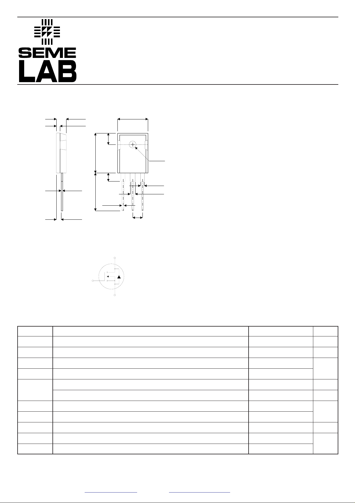
TO–247AD Package Outline.
D
S
G
Dimensions in mm (inches)
4.69 (0.185)
5.31 (0.209)
1.49 (0.059)
2.49 (0.098)
6.15
BSC
(0.242)
20.80 (0.819)
21.46 (0.845)
15.49 (0.610)
16.26 (0.640)
3.55 (0.140)
3.81 (0.150)
SML50B26F
N–CHANNEL
ENHANCEMENT MODE
HIGH VOLTAGE
POWER FREDFET
0.40 (0.016)
0.79 (0.031)
2.21 (0.087)
2.59 (0.102)
19.81 (0.780)
4.50
20.32 (0.800)
1.01 (0.040)
1.40 (0.055)
1
Max.
(0.177)
5.25 (0.215)
BSC
32
1.65 (0.065)
2.13 (0.084)
2.87 (0.113)
3.12 (0.123)
Pin 1 – Gate Pin 2 – Drain Pin 3 – Source
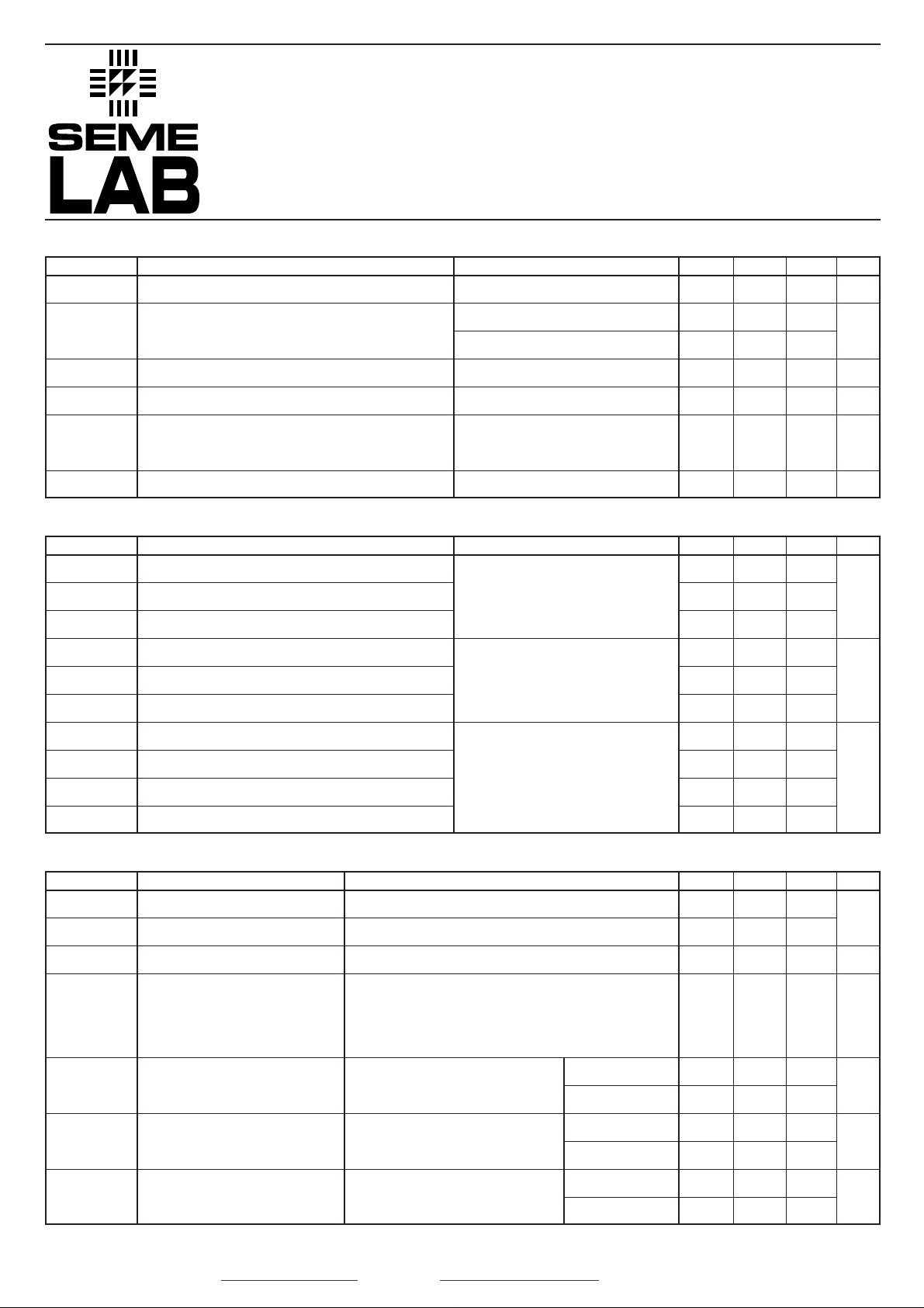
ABSOLUTE MAXIMUM RATINGS (T
V
I
I
V
V
P
D
DM
DSS
GS
GSM
D
Drain – Source Voltage
Continuous Drain Current
Pulsed Drain Current
1
Gate – Source Voltage
Gate – Source Voltage Transient
Total Power Dissipation @ T
Derate Linearly
= 25°C unless otherwise stated)
case
= 25°C
case
V
DSS
I
D(cont)
R
DS(on)
500V
26A
0.200
ΩΩ
• Faster Switching
• Lower Leakage
• 100% Avalanche Tested
• Popular TO–247 Package
• Fast Recovery Body Diode
StarMOS is a new generation of high voltage
N–Channel enhancement mode power MOSFETs.
This new technology minimises the JFET effect,
increases packing density and reduces the
on-resistance. StarMOS also achieves faster
switching speeds through optimised gate layout.
500
26
104
±20
±30
300
2.4
V
A
A
V
W
W/°C
TJ, T
T
L
I
AR
E
AR
E
AS
STG
Operating and Storage Junction Temperature Range
Lead Temperature : 0.063” from Case for 10 Sec.
1
Avalanche Current
Repetitive Avalanche Energy
Single Pulse Avalanche Energy
(Repetitive and Non-Repetitive)
1
2
1) Repetitive Rating: Pulse Width limited by maximum junction temperature.
2) Starting TJ= 25°C, L = 3.85mH, RG= 25Ω, Peak IL= 26A
Semelab plc. Telephone +44(0)1455 556565. Fax +44(0)1455 552612.
E-mail: sales@semelab.co.uk
Website: http://www.semelab.co.uk
–55 to 150
300
26
30
1300
°C
A
mJ
8/99
SML50B26F
STATIC ELECTRICAL RATINGS (T
Characteristic Test Conditions Min. Typ. Max. Unit
BV
DSS
Drain – Source Breakdown Voltage
Zero Gate Voltage Drain Current
I
DSS
I
GSS
V
GS(TH)
I
D(ON)
R
DS(ON)
(VGS= 0V)
Gate – Source Leakage Current
Gate Threshold Voltage
On State Drain Current
2
Drain – Source On State Resistance
DYNAMIC CHARACTERISTICS
Characteristic Test Conditions Min. Typ. Max. Unit
C
iss
C
oss
C
rss
Q
g
Q
gs
Q
gd
t
d(on)
t
r
t
d(off)
t
f
Input Capacitance
Output Capacitance
Reverse Transfer Capacitance
Total Gate Charge
3
Gate – Source Charge
Gate – Drain (“Miller”) Charge
Turn–on Delay Time
Rise Time
Turn-off Delay Time
Fall Time
= 25°C unless otherwise stated)
case
VGS= 0V , ID= 250µA
VDS= V
VDS= 0.8V
VGS= ±30V , VDS= 0V
VDS= VGS, ID= 1.0mA
VDS> I
VGS= 10V
2
VGS= 10V , ID= 0.5 ID[Cont.]
VGS= 0V
VDS= 25V
f = 1MHz
VGS= 10V
VDD= 0.5 V
ID= ID[Cont.] @ 25°C
VGS= 15V
VDD= 0.5 V
ID= ID[Cont.] @ 25°C
RG= 1.8Ω
DSS
DSS
D(ON)
, TC= 125°C
x R
DS(ON)
DSS
DSS
Max
500
V
25
µA
250
±100
24
26
0.20
nA
V
A
Ω
3700 4440
510 715
pF
200 300
150 225
25 37
nC
70 105
12 25
10 20
ns
50 75
815
SOURCE – DRAIN DIODE RATINGS AND CHARACTERISTICS
Characteristic Test Conditions Min. Typ. Max. Unit
I
I
V
S
SM
SD
Continuous Source Current
Pulsed Source Current
Diode Forward Voltage
1
2
(Body Diode)
(Body Diode)
VGS= 0V , IS= – ID[Cont.]
IS≤ ID[cont] dI / dt = 100A/µs
dv / dt
Peak Diode Recovery
V
DD ≤VDSS
VR= 200V
TJ≤ 150°C RG= 2.0Ω
IS= – ID[Cont.] TJ= 25°C
t
rr
Reverse Recovery Time
dI / dt = 100A/µsT
IS= – ID[Cont.] TJ= 25°C
Q
rr
Reverse Recovery Charge
dl / dt = 100A/µsT
IS= – ID[Cont.] TJ= 25°C
I
rrm
Peak Recovery Current
dl / dt = 100A/µsT
Semelab plc. Telephone +44(0)1455 556565. Fax +44(0)1455 552612.
E-mail: sales@semelab.co.uk
Website: http://www.semelab.co.uk
= 125°C
J
= 125°C
J
= 125°C
J
1.3
4.5
12
18
26
104
1.3
5
250
500
A
V
V/ns
ns
µC
A
8/99
 Loading...