

Characteristic Min. Typ. Max. Unit
1.00
50
R
q
JC
R
q
JA
Junction to Case
Junction to Ambient
°C/W
THERMAL CHARACTERISTICS
SML100C4
Semelab plc. Telephone +44(0)1455 556565. Fax +44(0)1455 552612.
E-mail: sales@semelab.co.uk
Website: http://www.semelab.co.uk
6/99
N–CHANNEL
ENHANCEMENT MODE
HIGH VOLTAGE
POWER MOSFETS
1) Repetitive Rating: Pulse Width limited by maximum junction temperature.
V
DSS
I
D
I
DM
V
GS
P
D
TJ, T
STG
T
L
Drain – Source Voltage
Continuous Drain Current
Pulsed Drain Current
1
Gate – Source Voltage
Total Power Dissipation @ T
case
= 25°C
Derate Linearly
Operating and Storage Junction Temperature Range
Lead Temperature : 0.063” from Case for 10 Sec.
1000
3.6
14.4
±30
125
1.0
-55 to +150
300
V
A
V
W
W/°C
°C
ABSOLUTE MAXIMUM RATINGS (T
case
= 25°C unless otherwise stated)
V
DSS
1000V
I
D(cont)
3.6A
R
DS(on)
4.00
WW
WW
• Faster Switching
• Lower Leakage
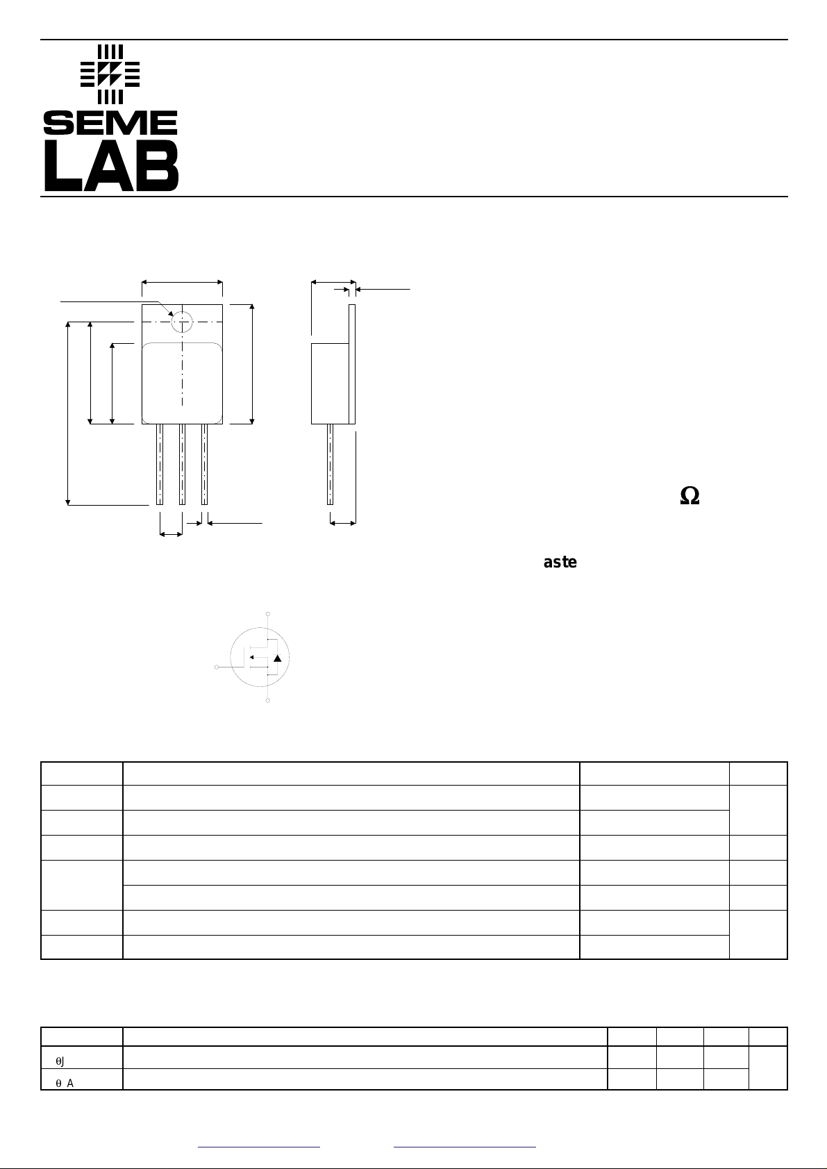
• TO–254 Hermetic Package
3.53 (0.139)
TO–254 Package Outline.
Dimensions in mm (inches)
Pin 1 – Drain Pin 2 – Source Pin 3 – Gate
3.78 (0.149)
16.89 (0.665)
17.40 (0.685)
30.35 (1.195)
31.40 (1.235)
13.59 (0.535)
13.84 (0.545)
Dia.
20.07 (0.790)
20.32 (0.800)
13.59 (0.535)
13.84 (0.545)
123
6.32 (0.249)
6.60 (0.260)
1.02 (0.040)
1.27 (0.050)
0.89 (0.035)
1.14 (0.045)
3.81 (0.150)
BSC
3.81 (0.150)
BSC
D
G
S
Characteristic Test Conditions Min. Typ. Max. Unit
Drain to Case Capacitance
Input Capacitance
Output Capacitance
Reverse Transfer Capacitance
Total Gate Charge
Gate – Source Charge
Gate – Drain (“Miller”) Charge
Turn–on Delay Time
Rise Time
Turn-off Delay Time
Fall Time
f = 1MHz
VGS= 0V
VDS= 25V
f = 1MHz
VGS= 10V
VDD= 0.5 V
DSS
ID= ID[Cont.] @ 25°C
VGS= 10V
VDD= 0.5 V
DSS
ID= ID[Cont.] @ 25°C
RG= 1.8
W
Characteristic Test Conditions Min. Typ. Max. Unit
3.6
14.4
1.3
290 580
1.65 3.3
I
S
I
SM
V
SD
t
rr
Q
rr
(Body Diode)
(Body Diode)
VGS= 0V , IS= – ID[Cont.]
IS= – ID[Cont.] , dls / dt = 100A/µs
IS= – ID[Cont.] , dls / dt = 100A/µs
Continuous Source Current
Pulsed Source Current
1
Diode Forward Voltage
2
Reverse Recovery Time
Reverse Recovery Charge
A
V
ns
µC
SOURCE – DRAIN DIODE RATINGS AND CHARACTERISTICS
C
DC
C
iss
C
oss
C
rss
Q
g
Q
gs
Q
gd
t
d(on)
t
r
t
d(off)
t
f
pF
pF
nC
ns
DYNAMIC CHARACTERISTICS
Characteristic Test Conditions Min. Typ. Max. Unit
SML100C4
Semelab plc. Telephone +44(0)1455 556565. Fax +44(0)1455 552612.
E-mail: sales@semelab.co.uk
Website: http://www.semelab.co.uk
6/99
Characteristic Min. Typ. Max. Unit
125
125
3.6
SOA1
SOA2
I
LM
Safe Operating Area
Safe Operating Area
Inductive Current Clamped
VDS= 0.4V
DSS
, IDS= PD/ 0.4V
DSS
, t = 1 Sec.
IDS= ID[Cont.] , VDS= PD/ ID[Cont.] , t = 1 Sec.
W
A
SAFE OPERATING AREA CHARACTERISTICS
1) Repetitive Rating: Pulse Width limited by maximum junction temperature.
2) Pulse Test: Pulse Width < 380µS , Duty Cycle < 2%
CAUTION — Electrostatic Sensitive Devices. Anti-Static Procedures Must Be Followed.
BV
DSS
I
DSS
I
GSS
V
GS(TH)
I
D(ON)
R
DS(ON)
VGS= 0V , ID= 250µA
VDS= V
DSS
VDS= 0.8V
DSS
, TC= 125°C
VGS= ±30V , VDS= 0V
VDS= VGS, ID= 1.0mA
VDS> I
D(ON)
x R
DS(ON)
Max
VGS= 10V
VGS= 10V , ID= 0.5 ID[Cont.]
Drain – Source Breakdown Voltage
Zero Gate Voltage Drain Current
(VGS= 0V)
Gate – Source Leakage Current
Gate Threshold Voltage
On State Drain Current
2
Drain – Source On State Resistance
2
1000
250
1000
±100
24
3.6
4.00
V
µA
nA
V
A
W
STATIC ELECTRICAL RATINGS (T
case
= 25°C unless otherwise stated)
15 22
805 950
115 160
37 60
35 55
4.3 7
18 27
10 20
12 24
33 50
16 32
 Loading...