

Semelab Plc SML1001RHN Datasheet
SML1001RHN
SML901RHN0
Prelim. 7/98
Semelab plc. Telephone +44(0)1455 556565. Fax +44(0)1455 552612.
E-mail: sales@semelab.co.uk
Website: http://www.semelab.co.uk
SML
Parameter 901RHN 1001RHN Unit
Characteristic / Test Conditions / Part Number Min. Typ. Max. Unit
BV
DSS
I
DSS
I
GSS
I
D(ON)
V
GS(TH)
R
DS(ON)
V
DSS
I
D
I
DM
V
GS
P
D
TJ, T
STJ
T
L
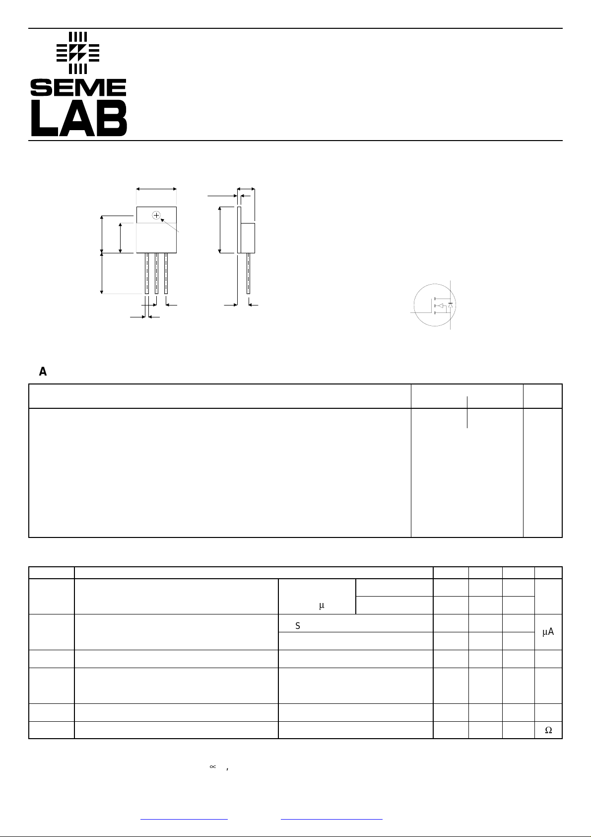
TO–258 Package Outline.
Dimensions in mm (Inches)
Drain – Source Voltage
Continuous Drain Current
Pulsed Drain Current
1
Gate – Source Voltage
Total Power Dissipation @ T
case
= 25°C
Derate above 25°C
Operating and Storage Junction Temperature Range
Lead Tempeature (0.063” from Case for 10 Sec.)
SML1001RHN
SML901RHN
900 1000
10
40
±30
250
2
–55 to +150°C
300
V
A
A
V
W
W/°C
°C
Drain – Source Breakdown Voltage
Zero Gate Voltage Drain Current
(VGS= 0V)
Gate – Source Leakage Current
On State Drain Current
2
Gate Threshold Voltage
Static Drain – Source On State Resistance
2
1000
900
250
1000
±100
10
24
1.00
V
m
A
nA
A
V
W
MAXIMUM RATINGS (T
case
=25°C unless otherwise stated)
1) Repetitive Rating: Pulse Width limited by maximum junction temperature.
2) Pulse Test: Pulse Width < 380µS , Duty Cycle < 2%
STATIC ELECTRICAL RATINGS (T
case
=25°C unless otherwise stated)
N–CHANNEL
ENHANCEMENT MODE
HIGH VOLTAGE
POWER MOSFETS
4TH GENERATION MOSFET
D
G
S
VGS= 0V
ID= 250mA
VDS= V
DSS
VDS= 0.8V
DSS
TC= 125°C
VGS= ±30V VDS= 0V
VDS> I
D(ON)
x R
DS(ON)
Max
VGS= 10V
VDS= V
GS
ID= 1.0mA
VGS= 10V , ID= 0.5 ID[Cont.]
Pin 1 – Drain Pin 2 – Source Pin 3 – Gate
6.86 (0.270)
17.65 (0.695)
17.39 (0.685)
4.19 (0.165)
3.94 (0.155)
17.96 (0.707)
17.70 (0.697)
13.84 (0.545)
19.05 (0.750)
12.70 (0.500)
123
13.58 (0.535)
5.08 (0.200)
1.65 (0.065)
1.39 (0.055)
Typ.
Dia.
BSC
1.14 (0.707)
0.88 (0.035)
21.21 (0.835)
20.70 (0.815)
6.09 (0.240)
3.56 (0.140)
BSC
SML1001RHN
SML901RHN0
Prelim. 7/98
Semelab plc. Telephone +44(0)1455 556565. Fax +44(0)1455 552612.
E-mail: sales@semelab.co.uk
Website: http://www.semelab.co.uk
Characteristic Test Conditions. Min. Typ. Max. Unit
C
iss
C
oss
C
rss
Q
g
Q
gs
Q
gd
t
d(on)
t
r
t
d(off)
t
f
Characteristic / Test Conditions. Part Number Min. Typ. Max. Unit
10
40
1.3
320 636 1200
2.2 4.5 9
I
S
I
SM
V
SD
t
rr
Q
rr
Continuous Source Current (Body Diode)
Pulsed Source Current1(Body Diode)
Diode Forward Voltage
2
Reverse Recovery Time
Reverse Recovery Charge
VGS= 0V
IS= – ID[Cont.]
IS= – ID[Cont.]
dls / dt = 100A/ms
A
A
V
ns
µC
Characteristic / Test Conditions / Part Number Min. Typ. Max. Unit
250
250
40
SOA1
SOA2
I
LM
VDS= 0.4 V
DSS
, IDS= PD/ 0.4 V
DSS
, t = 1 Sec
IDS= IDS[Cont.] , VDS= PD/ ID[Cont.] , t = 1 Sec
Safe Operating Area
Safe Operating Area
Inductive Current Clamped
W
A
Characteristic / Test Conditions. Min. Typ. Max. Unit
0.50
40
R
q
JC
Junction to Case
Junction to Ambient
°C/W
°C/W
DYNAMIC CHARACTERISTICS
SOURCE – DRAIN DIODE RATINGS AND CHARACTERISTICS
SAFE OPERATING AREA CHARACTERISTICS
THERMAL CHARACTERISTICS (T
case
=25°C unless otherwise stated)
1) Repetitive Rating: Pulse Width limited by maximum junction temperature.
2) Pulse Test: Pulse Width < 380µS , Duty Cycle < 2%
3) See MIL–STD–750 Method 3471
Input capacitance
Output capacitance
Reverse transfer capacitance
Total Gate Charge
3
Gate – Source Charge
Gate – Drain (“Miller”) Charge
Turn–on Delay Time
Rise Time
Turn-off Delay Time
Fall Time
VGS= 0V
VDS= 25V
f = 1MHz
VGS= 10V
ID= ID[Cont.]
VDD= 0.5 V
DSS
VDD= 0.5 V
DSS
ID= ID[Cont.]
VGS= 15V
RG= 1.8
W
pF
nC
ns
2460 2950
360 500
105 160
90 130
9.3 14
47 70
15 30
16 32
64 95
24 48
 Loading...