

Semelab Plc LT1085SMD, LT1085-T257, LT1085IG-12 Datasheet
Semelab plc. Telephone +44(0)1455 556565. Fax +44(0)1455 552612.
E-mail: sales@semelab.co.uk
Website: http://www.semelab.co.uk
Prelim. 7/00
LT1085GMD
LT1085IGDII
LT1085SMD
ABSOLUTE MAXIMUM RATINGS (T
case
= 25°C unless otherwise stated)
DEVICE
(1)
PACKAGE
LT1085K–XX TO–3
LT1085G–XX TO–257
LT1085IG–XX Isolated TO–257
LT1085SMD–XX SMD1
DESCRIPTION
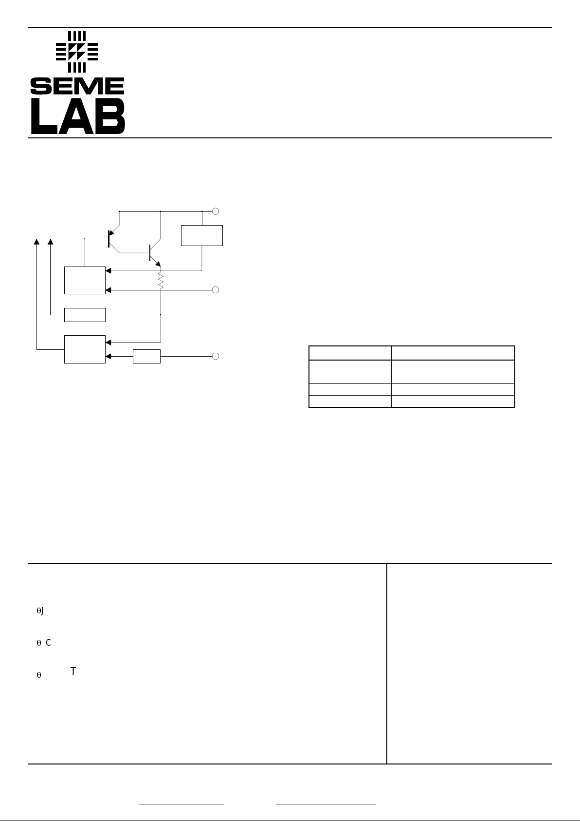
The LT1085 voltage regulators are monolithic integrated circuits designed for use in applications
requiring a well regulated positive output voltage
with low input-output differential voltage.
Features include full power usage of up to 3A load current, internal current limiting and thermal shutdown. Safe area
protection on the die is also included, providing protection of the series pass Darlington transistor under most conditions.
The hermetically sealed TO–3 packages are utilised for high reliablitiy and low thermal resistance, whilst the SMD1
package is designed for surface mount applications.
Note
1) –XX = Voltage Option: 3.3, 5 or 12
–XX = Left blank for Adjustable Option.
3 AMP POSITIVE
VOLTAGE REGULATOR
V
IN
Input – Output Voltage Differential
P
D
Power Dissipation
R
q
JC
Thermal Resistance Junction To Case TO–3 Control
TO–3 Power
R
q
JC
Thermal Resistance Junction To Case SMD1 Control
SMD1 Power
R
q
JC
Thermal Resistance Junction To Case TO–257 Control
TO–257 Power
T
J
Operating Junction Temperature Range Control
Power
T
STG
Storage Temperature Range
T
LEAD
Lead Temperature (for 10 sec.)
35V
Internally limited *
0.93°C / W
3.0°C / W
0.79°C / W
4.0°C / W
0.79°C / W
4.0°C / W
–55 to 150°C
–55 to 200°C
–65 to 150°C
300°C
FEATURES
• Low Dropout Performance
• Fixed or Adjustable Voltages
• Fixed Output Voltages of 3.3V, 5V & 12V
• Adjustable Output Voltage Range From 1.2V
• Line Regulation 0.015% / V Typical.
• Load Regulation 0.01% Typical.
• Available in Hermetically Sealed TO–3, SMD1 and
TO–257 (isolated & non-isolated) Packages.
• Military Temperature Range (–55 to +150°C)
INPUT
SAFE AREA
PROTECTION
THERMAL
OVER LO AD
CURRENT
LIMITING
AMPLIFIER
VOLTAGE
REGUL ATION
AMPLIFIER
OUTPUT
ADJUST
LIMIT
SENSE
V
REF
* These ratings are only applicable for power dissipations of 30 Watts over a limited range of VIN– V
OUT
.
Semelab plc. Telephone +44(0)1455 556565. Fax +44(0)1455 552612.
E-mail: sales@semelab.co.uk
Website: http://www.semelab.co.uk
Prelim. 7/00
LT1085GMD
LT1085IGDII
LT1085SMD
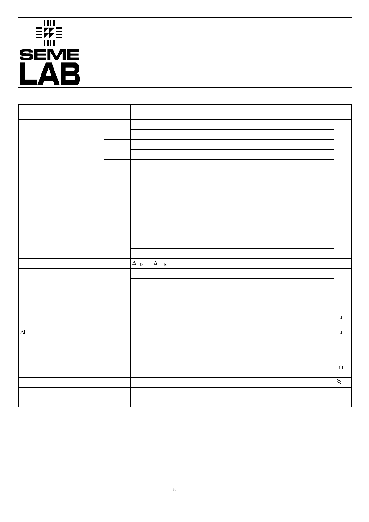
V
O
4
Output Voltage
V
REF
4
Reference Voltage
REG
(LINE)
4
Line Regulation
REG
(LOAD)
4
Load Regulation
V
D
Dropout Voltage
I
CL
Current Limit
I
Q
Quiescent Current
REG
(THERM)
Thermal Regulation
I
PIN
Adjust Pin Current
D
I
PIN
Adjust Pin Current Change
T
S
Temperature Stability
I
O
Minimum Load Current
V
N
RMS Output Noise
5
R
A
Ripple Rejection Ratio
6
VIN– V
OUT
= 6.3V IO= 10mA
I
O
= 10mA to 3A TJ= Over Temp
3
VIN– V
OUT
= 8V IO= 10mA
I
O
= 10mA to 3A TJ= Over Temp
3
VIN– V
OUT
= 15V IO= 10mA
I
O
= 10mA to 3A TJ= Over Temp
3
VIN– V
OUT
= VO+ 3V IO= 10mA
I
O
= 10mA to 3A TJ= Over Temp
3
VIN– V
OUT
= 1.5 to 15V TJ= 25°C
I
O
= 10mA TJ= Over Temp
3
VIN– V
OUT
= 1.5 to 35V IO= 10mA
T
J
= Over Temp
3
VIN– V
OUT
= 3V TJ= 25°C
V
IN
– V
OUT
= 3V TJ= Over Temp
3
D
V
OUT
, DV
REF
= 1% TJ= Over Temp
3
VIN– V
OUT
= 5V TJ= Over Temp
3
VIN– V
OUT
= 25V TJ= Over Temp
3
VIN– V
OUT
= 35V TJ= Over Temp
3
tp= 30ms TJ= 25°C
T
J
= 25°C
T
J
= Over Temp
3
TJ= Over Temp
3
VIN– V
OUT
= 5V IO= 0.5A
T
J
= Over Temp
3
VIN– V
OUT
= 25V IO= 0.5A
T
J
= Over Temp
3
TJ= 25°C
V
IN
– V
OUT
= 3V IO= 3A
T
J
= Over Temp
3
3.267 3.3 3.333
3.234 3.3 3.366
4.95 5 5.05
4.90 5 5.10
11.88 12 12.12
11.76 12 12.24
1.238 1.25 1.262
1.225 1.25 1.270
0.015 0.2
0.035
0.05 0.6
0.1 0.3
0.2 0.4
1.3 1.5
3.2 4.0
0.2 0.5
10
0.002 0.01
55
120
0.2 5
0.5
510
0.003
60 75
3.3
5
12
ADJ.
Output
Parameter Voltage Test Conditions
1,2
Min. Typ. Max. Unit
ELECTRICAL CHARACTERISTICS (T
J
= 25°C Unless otherwise stated)
V
V
%
%
%
V
A
mA
% / W
m
A
m
A
%
mA
%V
O
dB
Notes
1. Test Conditions unless otherwise stated: VIN= 1.5 to 35V, or Maximum Input, whichever is less.
I
O
= 10mA to 3A.
2. These specifications are only applicable for power dissipations of 30 Watts over a limited range of V
IN
– V
OUT
.
3. Over Temp. = Over specified Junction Temperature Range (See Absolute Maximum Ratings).
4. Low duty cycle pulse test with Kelvin connections required. Changes in output voltage are covered under the specification
for thermal regulation.
5. Bandwidth of 10Hz to 10kHz.
6. 120Hz input ripple, 15V = 64dB min. C
OUT(CADJ
) = 25mF.
 Loading...