

Semelab Plc LT1085LCC4 Datasheet
Prelim. 8/00
LT1085LCC4
MILITARY VERSION
Semelab plc. Telephone +44(0)1455 556565. Fax +44(0)1455 552612.
E-mail: sales@semelab.co.uk
Website: http://www.semelab.co.uk
1.39 (0.055)
1.15 (0.045)
0.76 (0.030)
0.51 (0.020)
1.39 (0.055)
1.02 (0.040)
15
16
13
12
14
34
56
7
17
18
1
2
11
10
8
9
9.14 (0.360)
8.64 (0.340)
1.27 (0.050)
1.07 (0.040)
≈2.16 (0.085)
7.62 (0.300)
7.12 (0.280)
1.65 (0.065)
1.40 (0.055)
0.33 (0.013)
0.08 (0.003)
0.43 (0.017)
0.18 (0.007
Rad.
Rad.
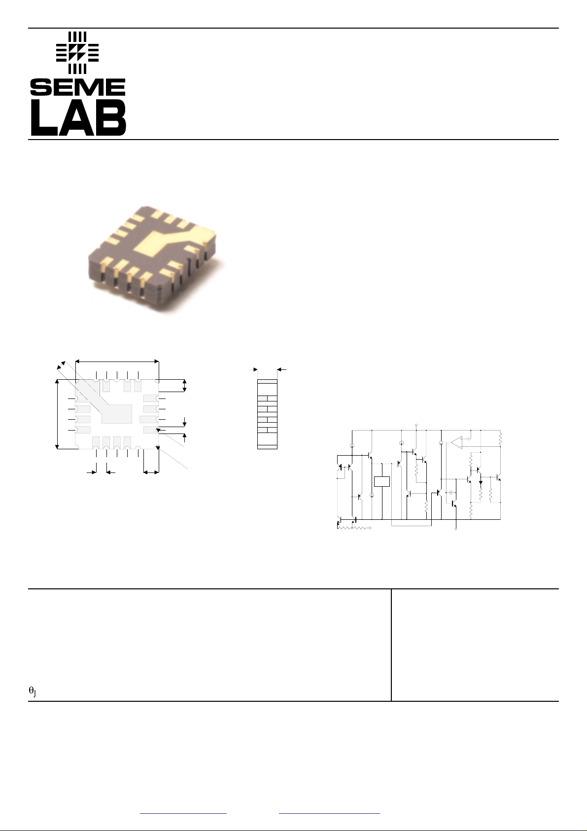
LCC4
ABSOLUTE MAXIMUM RATINGS (T
case
= 25°C unless otherwise stated)
CERAMIC SURFACE MOUNT
LOW DROPOUT POSITIVE ADJUSTABLE
VOLTAGE REGULATOR
FOR HI-REL APPLICATIONS
V
I-O
Input–Output Differential Voltage
P
D
Power Dissipation
V
IN
Operating Input Voltage
T
J
Operating Junction Temperature Range Control
Power
T
STG
Storage Temperature Range
q
JC
Thermal Resistance (junction to case)
30V
Internally limited
25V
–55 to 150°C
–55 to 200°C
–65 to 150°C
13°C/W
FEATURES
• Ceramic Surface Mount Hermetic Package
• Low Dropout Performance
• Output Current 3A
• Line Regulation 0.015% / V Typical.
• Load Regulation 0.1% Typical.
• Full Temperature Range (–55 to +150°C)
IN
V
THERMAL
LIMIT
ADJ
V
OUT
V
* Although the devices’ maximum operating voltage is limited to 25V the devices are guaranteed to withstand transient
input voltages up to 30V. For input voltages greater than the maximum operating input voltage, some degradation of
specifications will occur.
BLOCK DIAGRAM
Pads 5,4 = adjust
Pads 6,7,8,9,10,11,13 = Vin
Pads 1,2,15,16,17,18 = Vout
MECHANICAL DATA
Dimensions in mm (inches)
Parameter Test Conditions Min. Typ. Max. Unit
Prelim. 8/00
LT1085LCC4
MILITARY VERSION
Semelab plc. Telephone +44(0)1455 556565. Fax +44(0)1455 552612.
E-mail: sales@semelab.co.uk
Website: http://www.semelab.co.uk
V
REF
Reference Voltage
REG
(LINE)
Line Regulation
REG
(LOAD)
Load Regulation
See notes 1,2
V
D
Dropout Voltage
See note 3
I
CL
Current Limit
I
Q
Quiescent Current
Minimum Load Current
4
REG
(THERM)
Thermal Regulation
R
A
Ripple Rejection
I
PIN
Adjust Pin Current
D
I
PIN
Adjust Pin Current Change
T
S
Temperature Stability
Long Term Stability
V
N
RMS Output Noise
VIN– V
OUT
= 3V IO= 10mA
VIN– V
OUT
= 1.5 to 15V IO= 10mA to 3A
TJ= –55 to 125°C
IO= 10mA (VIN–V
OUT
) = 1.5 to 15V
TJ= –55 to 125°C
IO= 10mA (VIN–V
OUT
) = 15 to 30V
TJ= –55 to 125°C
VIN– V
OUT
= 3V
IO= 10mA to 3A TJ= –55 to 125°C
D
V
REF
= 1%
I
OUT
= 3A TJ= –55 to 125°C
VIN– V
OUT
= 5V TJ= –55 to 125°C
VIN– V
OUT
= 25V TJ= –55 to 125°C
VIN– V
OUT
= 5V TJ= –55 to 125°C
TP= 30ms TA= 25°C
f = 120Hz VIN– V
OUT
= 3V
IO= 3A C
ADJ
= 25mF
TJ= –55 to 125°C
VIN– V
OUT
= 1.5 to 15V
IO= 10mA to 3A TJ= –55 to 125°C
TJ= –55 to 125°C
TA= 125°C T = 1000 Hrs
f = 10Hz to 10kHz TA= 25°C
1.238 1.250 1.252
1.225 1.25 1.270
0.015 0.2
0.5
0.1 0.3
0.2 0.4
1.3 1.5
3.2 4
0.2 0.5
510
0.004 0.02
60 75
55 120
0.2 5
0.5
0.3
0.003
ELECTRICAL CHARACTERISTICS (Pre Irradiation) (T
J
= 25°C unless otherwise stated)
V
%
%
V
A
mA
%/W
dB
m
A
m
A
%
%
%
DESCRIPTION
The LT1085 is designed to provide 3A with higher efficiency than currently available devices. All internal circuitry is
designed to operate down to 1V input to output differential and the dropout voltage is fully specified as a function of load
current. Dropout is guaranteed at a maximum of 1.5V at maximum output current, decreasing at lower load currents. Onchip trimming adjusts the reference output voltage to 1%. Current limit is also trimmed, minimising the stress on both the
regulator and power source circuitry under overload conditions.
Notes:
1 Load and line regulation are measured at a constant junction temperature by low duty cycle pulse testing.
2 Power dissipation is determined by the input - output differential and the output current. Guaranteed maximum power
2 dissipation will not be available over the full input - output voltage range.
3 Dropout voltage is specified over the full output current range of the device.
 Loading...