

Semelab Plc LM137H-BSS2, LM137H, LM137MHVH, LM137MAHVH, LM137MAH Datasheet
...
IP137MAHVH
IP137MHVHA
LM137HVH
IP137MAH
IP137MH
LM137H
Prelim. 7/00
Semelab plc. Telephone +44(0)1455 556565. Fax +44(0)1455 552612.
E-mail: sales@semelab.co.uk
Website: http://www.semelab.co.uk
0.5 AMP
NEGATIVE ADJUSTABLE
VOLTAGE REGULATOR
V
I–O
Input - Output Differential Voltage – Standard
– HV Series
I
O
Output Current
P
D
Power Dissipation
T
J
Operating Junction Temperature Range
T
STG
Storage Temperature
T
J
Lead temperature
40V
50V
Internally limited
Internally limited
–55 to +150°C
–65 to 150°C
300°C
ABSOLUTE MAXIMUM RATINGS (T
case
= 25°C unless otherwise stated)
FEATURES
• –1.2V TO 47V OUTPUT VOLTAGE RANGE
• 0.5A OUTPUT CURRENT
• 1% OUTPUT VOLTAGE TOLERANCE
• 0.5% / A LOAD REGULATION
• 0.01%/V LINE REGULATION
• 0.02%/W THERMAL REGULATION
• INTERNAL PROTECTION
Internal current and power limiting coupled with
true thermal limiting prevents device damage
due to overloads or shorts, even if the regulator
is not fastened to a heat sink.
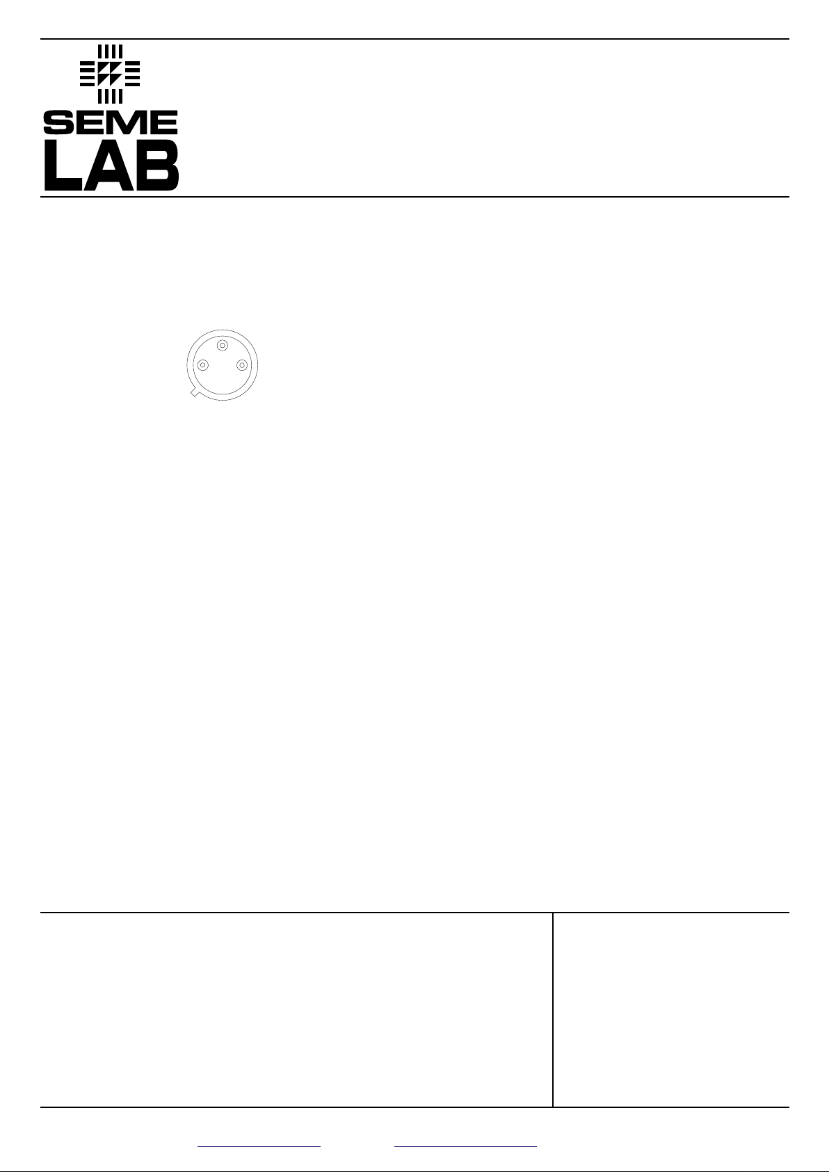
Pin 1 – ADJ.
Pin 2 – V
OUT
Pin 3 – V
IN
H Package – TO–39
1
2
3
IP137MAHV IP137MHV , IP137M
IP137MA LM137HV , LM137
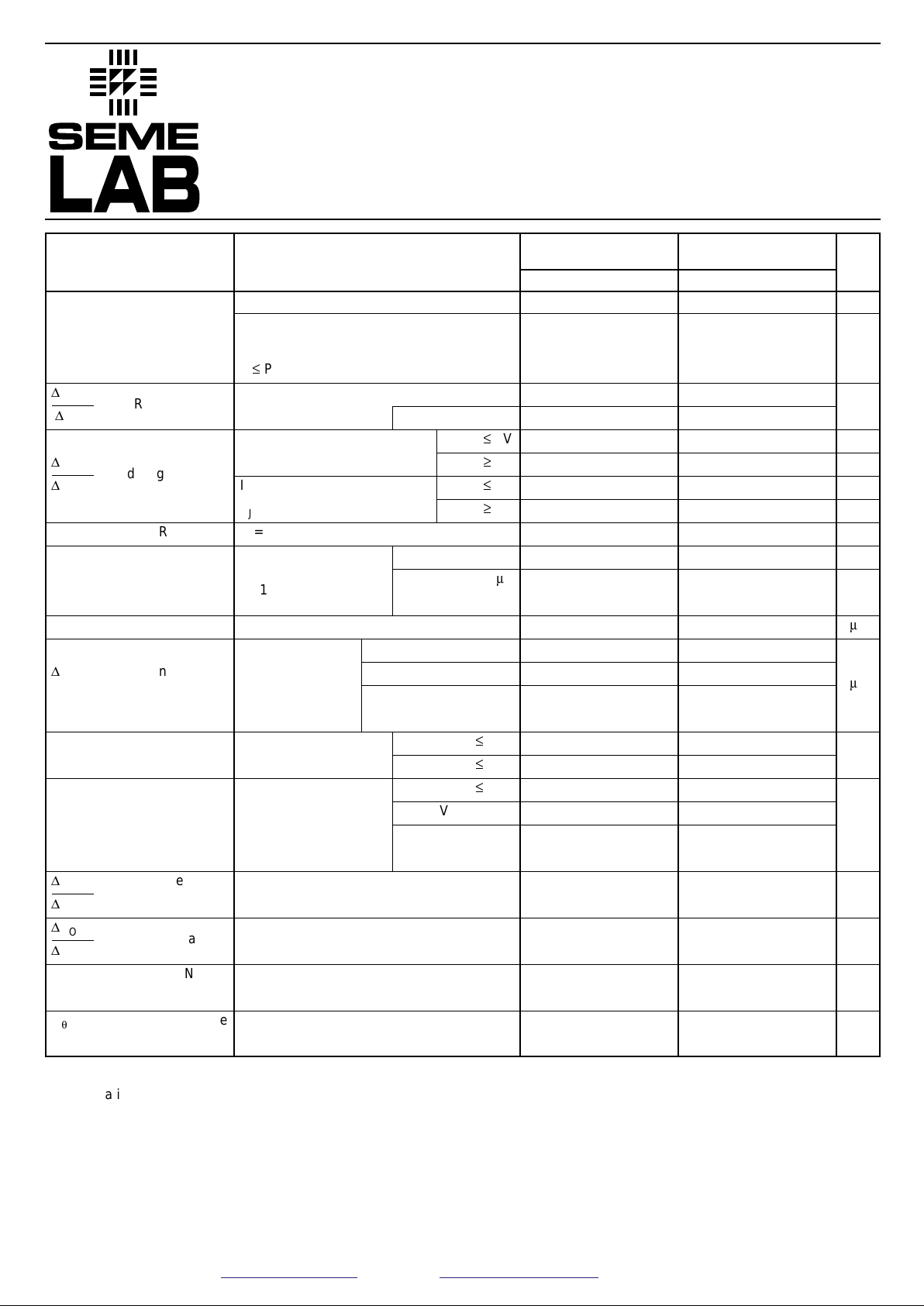
Parameter Test Conditions Min. Typ. Max. Min. Typ. Max. Units
I
OUT
= 10mA
I
OUT
= 10mA to I
MAX
VIN– V
OUT
= 3V to V
MAX
P£P
MAX
TJ= -55 to 150°C
V
IN
– V
OUT
= 3V to V
MAX
TJ= -55 to 150°C
I
OUT
= 10mA to I
MAX
V
OUT
£
5V
V
OUT
³
5V
I
OUT
= 10mA to I
MAX
V
OUT
£
5V
T
J
= -55 to 150°C V
OUT
³
5V
t
p
= 10ms TA= 25°C
C
ADJ
= 0
V
OUT
= -10V
C
ADJ
= 10mF
f = 120Hz
T
J
= -55 to 150°C
T
J
= -55 to 150°C
I
OUT
= 10mA to I
MAX
VIN– V
OUT
= 3V to 40V
T
J
= -55 to +150°C
V
IN
– V
OUT
= 3V to 50V
(HV SERIES)
VIN– V
OUT
£
40V
T
J
= -55 to 150°C
V
IN
– V
OUT
£
10V
V
IN
– V
OUT
£
15V
V
IN
– V
OUT
= 40V
T
J
= -55 to 150°C
V
IN
– V
OUT
= 50V
(HV SERIES)
TJ= -55 to 150°C
TA= +125°C
t = 1000 Hrs
f = 10 Hz to 10 kHz
T
A
= 25°C
H Package
IP137MAHVH
IP137MHVHA
LM137HVH
IP137MAH
IP137MH
LM137H
Prelim. 7/00
Semelab plc. Telephone +44(0)1455 556565. Fax +44(0)1455 552612.
E-mail: sales@semelab.co.uk
Website: http://www.semelab.co.uk
-1.225 -1.25 -1.275
-1.200 -1.25 -1.300
0.010 0.020
0.020 0.050
15 25
0.3 0.5
20 50
0.3 1
0.002 0.02
60
66 77
65 100
0.5 5
25
36
2.5 5
1.2 3
0.50 0.80 1.5
0.15 0.17
0.10 0.17 0.5
0.6
0.3 1
0.003
12 15
-1.238 -1.25 -1.262
-1.220 -1.25 -1.280
0.005 0.010
0.010 0.030
525
0.1 0.5
10 50
0.2 1
0.002 0.020
60 66
70 80
65 100
0.2 2
1.0 5
2.0 6
2.5 5
1.2 3
0.50 0.80 1.5
0.15 0.17
0.10 0.17 0.5
0.6 1.5
0.3 1
0.003
12 15
V
REF
Reference Voltage
D
V
OUT
Line Regulation
1
D
V
IN
D
V
OUT
Load Regulation
1
D
I
OUT
Thermal Regulation
Ripple Rejection
I
ADJ
Adjust Pin Current
D
I
ADJ
Adjust Pin Current
Change
I
MIN
Minimum Load
Current
I
CL
Current Limit
D
V
OUT
Temperature
D
TEMP Stability
D
V
OUT
Long Term Stability
D
TIME
e
n
RMS Output Noise
(% of V
OUT
)
R
q
JC
Thermal Resistance
Junction to Case
V
V
%/V
mV
%
mV
%
%/W
dB
dB
m
A
m
A
mA
A
%
%
%
°C/W
1) Regulation is measured at constant junction temperature, using pulse testing at a low duty cycle. Changes in output voltage due to
heating effects are covered under thermal regulation specifications. Load regulation is measured at a point
1
/8” from the bottom of
the package for the TO–3 and TO–66 packages, at the junction of the wide and narrow portion of the output lead for the
SMD1package, and
1
/8” below the base of the package on the output pin of the TO–257 package.
2) Test Conditions unless otherwise stated: V
IN
– V
OUT
= 5V , I
OUT
= 0.1A , P
MAX
= 2W , I
MAX
= 0.5A
V
MAX
= 40V for standard series , 50V for HV series.
 Loading...