

Semelab Plc IRFY140 Datasheet
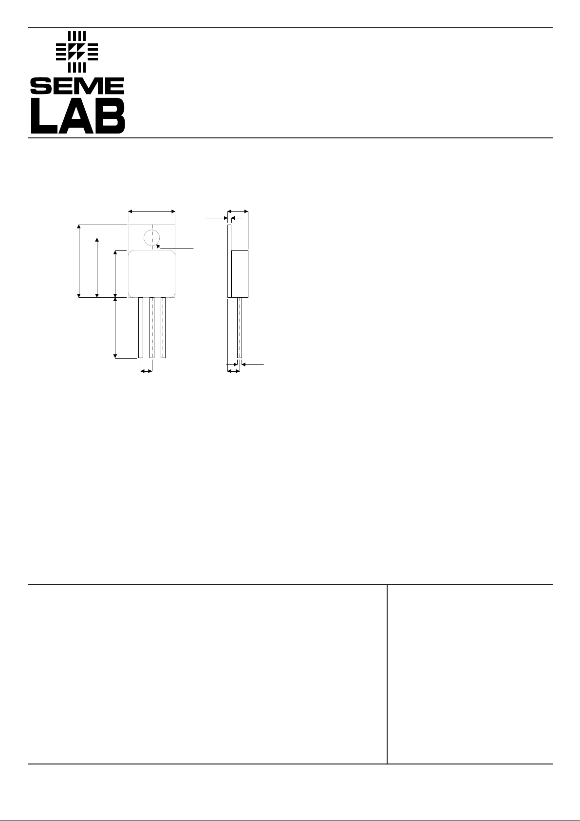
MECHANICAL DATA
Dimensions in mm (inches)
IRFY140
N–CHANNEL
4.70
0.70
0.90
5.00
16.38
16.89
10.41
10.67
3.56
Dia.
3.81
13.39
13.64
10.41
10.92
123
12.70
19.05
0.89
1.14
2.54
BSC
2.65
2.75
TO–220M – Metal Package
Pad 1 – Gate Pad 2 – Drain Pad 3 – Source
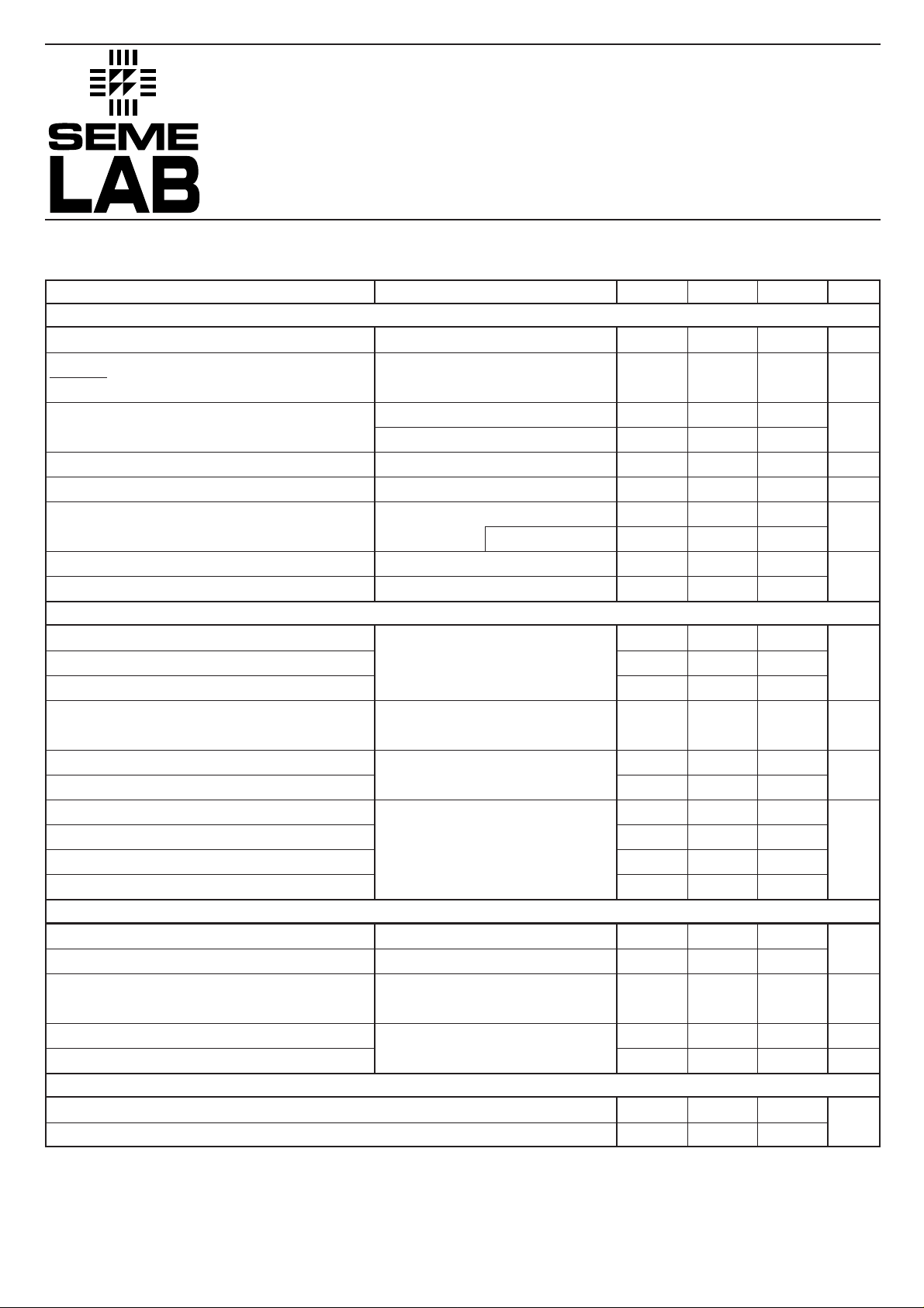
POWER MOSFET
FOR HI–REL
APPLICATIONS
V
DSS
I
D(cont)
R
DS(on)
FEATURES
• HERMETICALLY SEALED TO–220 METAL
PACKAGE
• SIMPLE DRIVE REQUIREMENTS
• LIGHTWEIGHT
• SCREENING OPTIONS AVAILABLE
• ALL LEADS ISOLATED FROM CASE
100V
18A
0.092
ΩΩ
ABSOLUTE MAXIMUM RATINGS (T
V
I
I
I
P
GS
D
D
DM
D
Gate – Source Voltage
Continuous Drain Current @ T
Continuous Drain Current @ T
Pulsed Drain Current
Power Dissipation @ T
case
= 25°C
= 25°C unless otherwise stated)
case
= 25°C
case
= 100°C
case
Linear Derating Factor
T
R
R
, T
J
θJC
θJA
stg
Operating and Storage Temperature Range
Thermal Resistance Junction to Case
Thermal Resistance Junction to Ambient
Semelab plc. Telephone (01455) 556565. Telex: 341927. Fax (01455) 552612.
±20V
18A
12A
72A
50W
0.48W/°C
–55 to 150°C
2.1°C/W max.
80°C/W max.
Prelim. 9/95
IRFY140
ELECTRICAL CHARACTERISTICS (T
Parameter Test Conditions Min. Typ. Max. Unit
STATIC ELECTRICAL RATINGS
BV
∆BV
∆T
R
DS(on)
V
GS(th)
g
fs
I
DSS
I
GSS
I
GSS
C
iss
C
oss
C
rss
Q
g
Q
gs
Q
gd
t
d(on)
t
r
t
d(off)
t
f
I
S
I
SM
V
SD
t
rr
Q
rr
L
D
L
S
Drain – Source Breakdown Voltage
DSS
Temperature Coefficient of
DSS
Breakdown Voltage
J
Static Drain – Source On–State
Resistance
Gate Threshold Voltage
Forward Transconductance
Zero Gate Voltage Drain Current
Forward Gate
Reverse Gate
– Source Leakage
– Source Leakage
DYNAMIC CHARACTERISTICS
Input Capacitance
Output Capacitance
Reverse Transfer Capacitance
Total Gate Charge
Gate – Source Charge
Gate – Drain (“Miller”) Charge
Turn–On Delay Time
Rise Time
Turn–Off Delay Time
Fall Time
SOURCE – DRAIN DIODE CHARACTERISTICS
Continuous Source Current
Pulse Source Current
Diode Forward Voltage
Reverse Recovery Time
Reverse Recovery Charge
PACKAGE CHARACTERISTICS
Internal Drain Inductance (from 6mm down drain lead pad to centre of die)
Internal Source Inductance (from 6mm down source lead to centre of source bond pad)
VGS= 0 ID= 1mA
Reference to 25°C
ID= 1mA
VGS= 10V ID= 12A
VGS= 10V ID= 18A
VDS= V
VDS≥ 15V IDS= 12A
VGS= 0 VDS= 0.8BV
VGS= 20V
VGS= –20V
VGS= 0
VDS= 25V
f = 1MHz
VGS= 10V ID= 18A
VDS= 0.5BV
ID= 18A
VDS= 0.5BV
VDD= 50V
ID= 18A
RG= 9.1Ω
IS= 18A TJ= 25°C
VGS= 0
IS= 18A TJ= 25°C
di/ dt≤ 100A/µsVDD≤ 50V
= 25°C unless otherwise stated)
C
GS
ID= 250µA
DSS
TJ= 125°C
DSS
DSS
100
0.1
V
V/°C
0.092
Ω
0.11
24
9.1
V
(Ω)
S(Ω
25
µA
250
100
nA
-100
1660
550
pF
120
30 59
nC
2.4 12
12 30.7
nC
21
145
ns
64
105
18
A
73
1.5
400
2.4
V
ns
µC
8.7
nH
8.7
Semelab plc. Telephone (01455) 556565. Telex: 341927. Fax (01455) 552612.
Prelim. 9/95
 Loading...