

Semelab Plc IRFM250 Datasheet
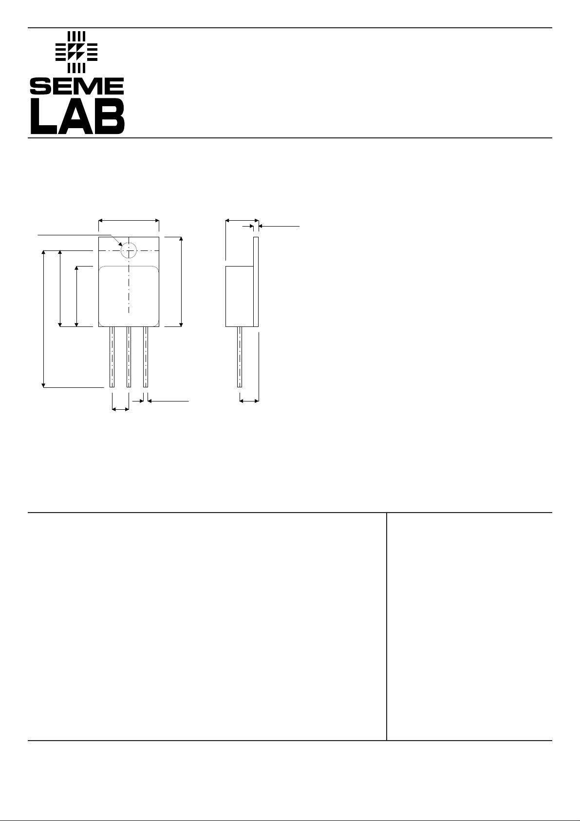
MECHANICAL DATA
Dimensions in mm (inches)
13.59 (0.535)
3.53 (0.139)
3.78 (0.149)
Dia.
13.84 (0.545)
6.32 (0.249)
6.60 (0.260)
1.02 (0.040)
1.27 (0.050)
IRFM250
N–CHANNEL
POWER MOSFET
V
DSS
I
D(cont)
200V
27.4A
20.07 (0.790)
20.32 (0.800)
3.81 (0.150)
BSC
30.35 (1.195)
31.40 (1.235)
16.89 (0.665)
17.40 (0.685)
13.59 (0.535)
13.84 (0.545)
3.81 (0.150)
123
0.89 (0.035)
1.14 (0.045)
BSC
TO–254AA – Isolated Metal Package
Pin 1 – Drain Pin 2 – Source Pin 3 – Gate
ABSOLUTE MAXIMUM RATINGS (T
V
GS
I
D
I
DM
P
D
I
L
dv / dt Peak Diode Recovery
Gate – Source Voltage
Continuous Drain Current @ VGS= 10V , TC = 25°C
Pulsed Drain Current
Max. Power Dissipation @ TC = 25°C
Linear Derating Factor
Avalanche Current , Clamped
2
C
@ V
1
R
DS(on)
FEATURES
• N–CHANNEL MOSFET
• HIGH VOLTAGE
• INTEGRAL PROTECTION DIODE
• HERMETIC ISOLATED TO-254 PACKAGE
• CERAMIC SURFACE MOUNT PACKAGE
OPTION
= 25°C unless otherwise stated)
= 10V , TC = 100°C
GS
0.100
±20V
27.4A
17A
110A
150W
1.2W / °C
27.4A
5.5V / ns
ΩΩ
R
θJC
R
θJA
R
θCS
, T
T
J
T
L
1) VDD= 50V , Starting TJ= 25°C , L ≥ 1mH , RG= 25Ω , Peak IL= 27.4A
2) ISD≤ 27.4A , di/dt ≤ 190A / µS , VDD≤ BV
Thermal Resistance Junction – Case
Thermal Resistance Junction – Ambient
Thermal Resistance Case – Sink
Operating Junction and Storage Temperature Range
STG
Lead Temperature (1.6mm from case for 10s)
, TJ≤ 150°C , Suggested RG= 2.35Ω
DSS
Semelab plc. Telephone (01455) 556565. Telex: 341927. Fax (01455) 552612.
0.83°C / W
48°C / W
0.21°C / W typ.
–55 to 150°C
300°C
Prelim. 9/95
IRFM250
ELECTRICAL CHARACTERISTICS (T
= 25°C unless otherwise stated)
J
Parameter Test Conditions Min. Typ. Max. Unit
STATIC ELECTRICAL RATINGS
BV
∆BV
∆T
Drain – Source Breakdown Voltage
DSS
Temperature Coefficient of
DSS
Breakdown Voltage
J
Static Drain – Source On–State
R
DS(on)
V
GS(th)
g
fs
I
DSS
I
GSS
I
GSS
Resistance
Gate Threshold Voltage
Forward Transconductance
Zero Gate Voltage Drain Current
Forward Gate
Reverse Gate
2
2
– Source Leakage
– Source Leakage
DYNAMIC CHARACTERISTICS
C
iss
C
oss
C
rss
C
DC
Q
g
Q
gs
Q
gd
t
d(on)
t
r
t
d(off)
t
f
Input Capacitance
Output Capacitance
Reverse Transfer Capacitance
Drain – Case Capacitance
Total Gate Charge
Gate – Source Charge
Gate – Drain (“Miller”) Charge
Turn– On Delay Time
Rise Time
Turn–Off Delay Time
Fall Time
SOURCE – DRAIN DIODE CHARACTERISTICS
I
I
V
t
Q
t
S
SM
SD
rr
rr
on
Continuous Source Current
Pulse Source Current
Diode Forward Voltage
Reverse Recovery Time
1
2
2
Reverse Recovery Charge
Forward Turn–On Time
2
PACKAGE CHARACTERISTICS
L
D
L
S
Internal Drain Inductance Measured from 6mm down drain lead to centre of die
Internal Source Inductance Measured from 6mm down source lead to source bond pad
1) Repetitive Rating – Pulse width limited by Maximum Junction Temperature
2) Pulse Test: Pulse Width ≤ 300µs, δ≤2%.
VGS= 0 ID= 1mA
Reference to 25°C
ID= 1mA
VGS= 10V ID= 17A
VGS= 10V ID= 27.4A
VDS= V
GS
ID= 250µA
VDS≥ 15V IDS= 27.4A
VGS= 0 VDS= 0.8BV
TJ= 125°C
VGS= 20V
VGS= –20V
VGS= 0
VDS= 25V
f = 1MHz
VGS= 10V
ID= 27.4A
VDS= 0.5BV
DSS
VDD= 100V
ID= 27.4A
RG= 2.35Ω
IS= 27.4A TJ= 25°C
VGS= 0
IF= 27.4A TJ= 25°C
di/ dt≤ 100A/µsVDD≤ 50V
Notes
DSS
200
0.28
V
V/°C
0.100
Ω
0.105
24
9
V
(Ω)
S(Ω
25
µA
250
100
nA
–100
3500
700
pF
110
12
55 115
822
nC
30 60
35
190
ns
170
130
27.4
A
110
1.9
950
9.0
V
ns
µC
Negligible
8.7
nH
8.7
Semelab plc. Telephone (01455) 556565. Telex: 341927. Fax (01455) 552612.
Prelim. 9/95
 Loading...