

Semelab Plc IRFE9230 Datasheet
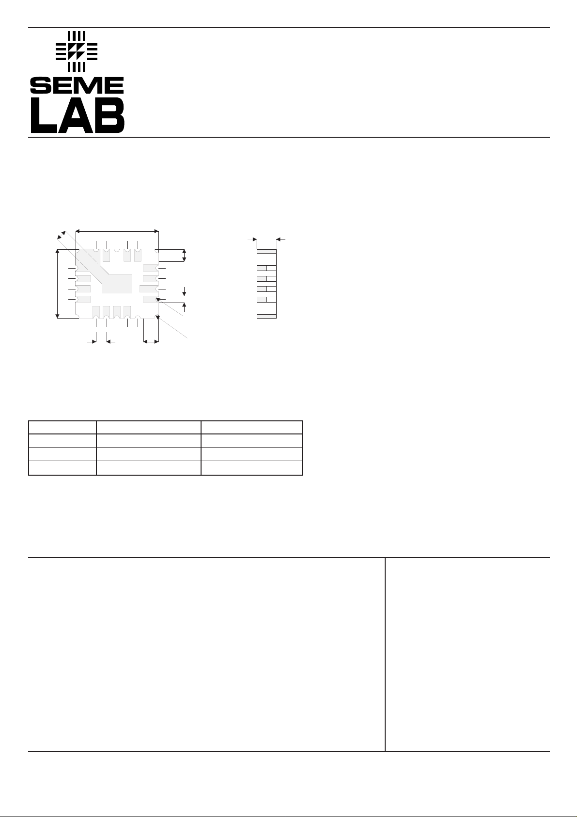
MECHANICAL DATA
Dimensions in mm (inches)
9.14 (0.360)
1.27 (0.050)
1.07 (0.040)
7.62 (0.300)
7.12 (0.280)
11
10
9
8
8.64 (0.340)
13
12
7
1.39 (0.055)
1.15 (0.045)
15
16
14
56
34
1.65 (0.065)
1.40 (0.055)
17
18
1
2
1.39 (0.055)
1.02 (0.040)
0.76 (0.030)
0.51 (0.020)
0.33 (0.013)
0.08 (0.003)
0.43 (0.017)
0.18 (0.007
Rad.
Rad.
≈2.16 (0.085)
P–CHANNEL
POWER MOSFET
V
DSS
I
D(cont)
R
DS(on)
FEATURES
IRFE9230
-200V
-3.6A
0.825
ΩΩ
LCC4
MOSFET TRANSISTOR PINS
GATE BASE 4,5
DRAIN COLLECTOR 1,2,15,16,17,18
SOURCE EMITTER 6,7,8,9,10,11,12,13
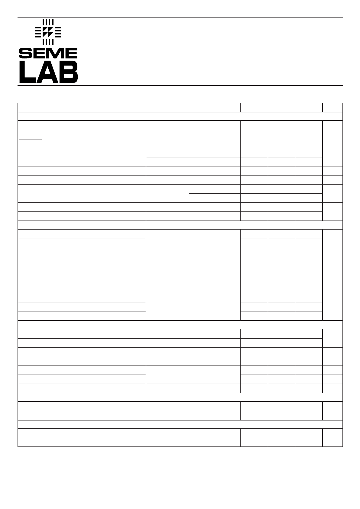
ABSOLUTE MAXIMUM RATINGS (T
V
I
I
I
P
GS
D
D
DM
D
Gate – Source Voltage
Continuous Drain Current @ T
Continuous Drain Current @ T
Pulsed Drain Current
Power Dissipation @ T
case
case
case
case
= 25°C
• SURFACE MOUNT
• SMALL FOOTPRINT
• HERMETICALLY SEALED
• DYNAMIC dv/dt RATING
• AVALANCHE ENERGY RATING
• SIMPLE DRIVE REQUIREMENTS
• LIGHT WEIGHT
= 25°C unless otherwise stated)
= 25°C
= 100°C
±20V
– 3.6A
– 2.2A
– 14.4A
22W
Linear Derating Factor
E
AS
Single Pulse Avalanche Energy
dv/dt Peak Diode Recovery
TJ, T
stg
Operating and Storage Temperature Range
3
2
– 55 to +150°C
Surface Temperature ( for 5 sec).
Semelab plc. Telephone +44(0)1455 556565. Fax +44(0)1455 552612. e-mail sales@semelab.co.uk
Website http://www.semelab.co.uk
0.17W/°C
75mJ
– 5V/ns
300°C
10/98
IRFE9230
ELECTRICAL CHARACTERISTICS (T
Parameter Test Conditions Min. Typ. Max. Unit
STATIC ELECTRICAL RATINGS
BV
∆BV
∆T
R
DS(on)
V
GS(th)
g
fs
I
DSS
I
GSS
I
GSS
C
iss
C
oss
C
rss
Q
g
Q
gs
Q
gd
t
d(on)
t
r
t
d(off)
t
f
I
S
I
SM
V
SD
t
rr
Q
rr
t
on
L
D
L
S
R
θJC
R
θJPC
Drain – Source Breakdown Voltage
DSS
Temperature Coefficient of
DSS
Breakdown Voltage
J
Static Drain – Source On–State
Resistance
1
Gate Threshold Voltage
Forward Transconductance
1
Zero Gate Voltage Drain Current
Forward Gate
Reverse Gate
– Source Leakage
– Source Leakage
DYNAMIC CHARACTERISTICS
Input Capacitance
Output Capacitance
Reverse Transfer Capacitance
Total Gate Charge
Gate – Source Charge
Gate – Drain (“Miller”) Charge
Turn–On Delay Time
Rise Time
Turn–Off Delay Time
Fall Time
SOURCE – DRAIN DIODE CHARACTERISTICS
Continuous Source Current
Pulse Source Current
Diode Forward Voltage
2
1
Reverse Recovery Time
Reverse Recovery Charge
1
Forward Turn–On Time
PACKAGE CHARACTERISTICS
Internal Drain Inductance (measured from 6mm down drain lead to centre of die)
Internal Source Inductance (from 6mm down source lead to source bond pad)
THERMAL CHARACTERISTICS
Thermal Resistance Junction – Case
Thermal Resistance Junction – PC Board
VGS= 0 ID= –1mA
Reference to 25°C
ID= –1mA
VGS= –10V ID= –2.2A
VGS= –10V ID= –3.6A
VDS= V
VDS≥ –15V IDS= –2.2A
VGS= 0 VDS= 0.8BV
VGS= –20V
VGS= 20V
VGS= 0
VDS= –25V
f = 1MHz
VGS= –10V
ID= –3.6A
VDS= 0.5BV
VDD= –100V
ID= –3.6A
RG= 7.5Ω
IS= –3.6A TJ= 25°C
VGS= 0
IF= –3.6A TJ= 25°C
di/ dt≤ –100A/µs VDD≤ –50V
= 25°C unless otherwise stated)
case
GS
ID= –250mA
DSS
TJ= 125°C
DSS
–200
– 0.22
0.80
0.825
– 2 – 4
2.2
– 25
– 250
– 100
100
700
200
40
14.7 34.8
0.8 7.0
5.0 17
50
100
100
80
–3.6
–14.4
–6.0
400
4.0
Negligible
1.8
4.3
5.8
19
V
V/°C
Ω
V
S (É)
µA
nA
pF
nC
ns
A
V
ns
µC
nH
°C/W
Notes
1) Pulse Test: Pulse Width ≤ 300ms, δ≤2%
2) Repetitive Rating – Pulse width limited by maximum junction temperature.
Semelab plc. Telephone +44(0)1455 556565. Fax +44(0)1455 552612. e-mail sales@semelab.co.uk
Website http://www.semelab.co.uk
10/98
 Loading...