

Semelab Plc IRF9130 Datasheet
IRF9130
Prelim. 10/99
Semelab plc. Telephone +44(0)1455 556565. Fax +44(0)1455 552612.
E-mail: sales@semelab.co.uk
Website: http://www.semelab.co.uk
V
GS
Gate – Source Voltage
I
D
Continuous Drain Current (VGS= 0 , T
case
= 25°C)
I
D
Continuous Drain Current (VGS= 0 , T
case
= 100°C)
I
DM
Pulsed Drain Current
1
P
D
Power Dissipation @ T
case
= 25°C
Linear Derating Factor
E
AS
Single Pulse Avalanche Energy
2
I
AR
Avalanche Current
1
E
AR
Repetitive Avalanche Energy
1
dv/dt Peak Diode Recovery
3
TJ, T
stg
Operating and Storage Temperature Range
T
L
Lead Temperature 1.6mm (0.63”) from case for 10 sec.
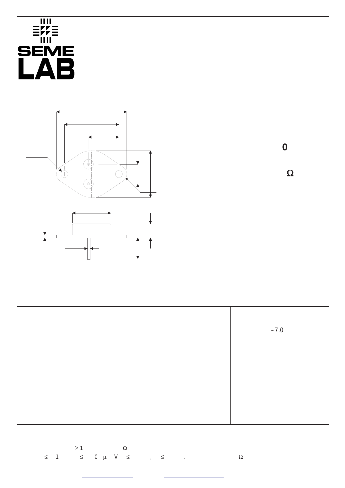
MECHANICAL DATA
Dimensions in mm (inches)
P–CHANNEL
POWER MOSFET
ABSOLUTE MAXIMUM RATINGS (T
case
= 25°C unless otherwise stated)
FEATURES
• HERMETICALLY SEALED TO–3 METAL
PACKAGE
• SIMPLE DRIVE REQUIREMENTS
• SCREENING OPTIONS AVAILABLE
TO–3 Metal Package
Pin 1 – Gate Pin 2 – Source Case – Drain
Notes
1) Repetitive Rating – Pulse width limited by maximum junction temperature.
2) @ VDD= –25V , L ³1.0mH , RG= 25W, Peak IL= –11A , Starting TJ= 25°C
3) @ ISD£
–11A , di/dt £–140A/ms , VDD£
BV
DSS
, TJ£
150°C , Suggested RG= 7.5
W
V
DSS
–100V
I
D(cont)
–11A
R
DS(on)
0.2
WW
WW
±20V
–11A
–7.0A
–50A
75W
0.6W/°C
81mJ
–11A
7.5mJ
–5.5V/ns
–55 to +150°C
300°C
39.95 (1.573)
max.
30.40 (1.197)
30.15 (1.187)
17.15 (0.675)
16.64 (0.655)
4.09 (0.161)
3.84 (0.151)
dia.
2 plcs.
1.78 (0.070)
1.52 (0.060)
1.09 (0.043)
0.97 (0.038)
dia.
2 plcs.
2
1
20.32 (0.800)
18.80 (0.740)
dia.
11.18 (0.440)
10.67 (0.420)
12.07 (0.475)
max.
26.67 (1.050)
7.87 (0.310)
6.99 (0.275)
11.30 (0.445)
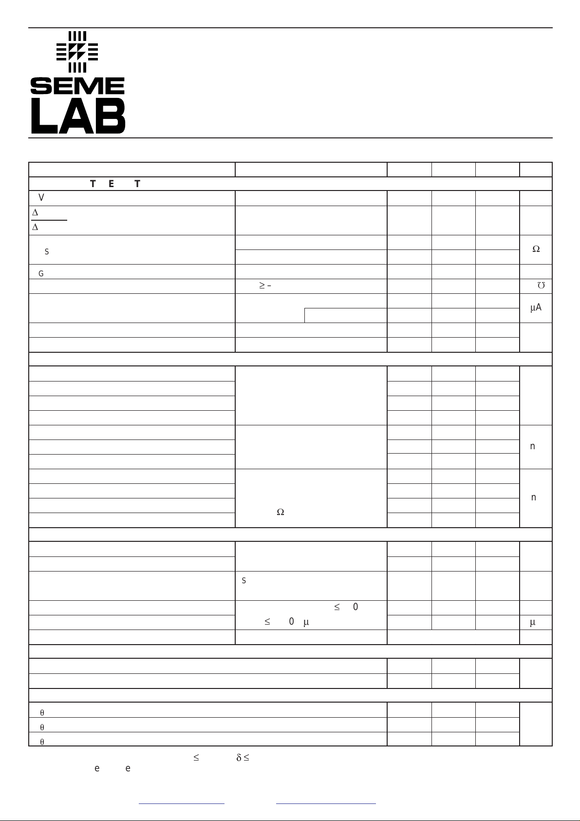
Parameter Test Conditions Min. Typ. Max. Unit
Drain – Source Breakdown Voltage
Temperature Coefficient of
Breakdown Voltage
Static Drain – Source On–State
Resistance
1
Gate Threshold Voltage
Forward Transconductance
Zero Gate Voltage Drain Current
Forward Gate
– Source Leakage
Reverse Gate
– Source Leakage
Drain to Case Capacitance
Input Capacitance
Output Capacitance
Reverse Transfer Capacitance
Total Gate Charge
Gate – Source Charge
Gate – Drain (“Miller”) Charge
Turn–On Delay Time
Rise Time
Turn–Off Delay Time
Fall Time
Continuous Source Current
Pulse Source Current
2
Diode Forward Voltage
Reverse Recovery Time
Reverse Recovery Charge
Forward Turn–On Time
IRF9130
Prelim. 10/99
Semelab plc. Telephone +44(0)1455 556565. Fax +44(0)1455 552612.
E-mail: sales@semelab.co.uk
Website: http://www.semelab.co.uk
–100
–0.087
0.3
0.35
–2 –4
3
–25
–250
–100
100
12
860
350
125
15 29
1.0 7.1
2.0 21
60
140
140
140
–11
–50
–4.7
250
3.0
Negligible
5.0
13
1.67
0.12
30
VGS= 0 ID= –1mA
Reference to 25°C
ID= –1mA
VGS= –10V ID= –7.0A
VGS= –10V ID= –11A
VDS= V
GS
ID= –250mA
VDS³
–15V IDS= –7.0A
VGS= 0 VDS= 0.8 x Max
TJ= 125°C
VGS= –20V
VGS= 20V
VGS= 0
VDS= – 25V
f = 1MHz
VGS= –10V
ID= –11A
VDS= 0.5 x max
VDD= –50V
ID= –11A
RG= 7.5
W
IS= –11A TJ= 25°C
VGS= 0
IF= –11A VDD£
–50V
di/ dt£
–100A/ms TJ= 25°C
ELECTRICAL CHARACTERISTICS (T
case
= 25°C unless otherwise stated)
V
V/°C
W
V
S (É)
m
A
nA
pF
nC
ns
A
V
ns
m
C
nH
°C/W
BV
DSS
D
BV
DSS
D
T
J
R
DS(on)
V
GS(th)
g
fs
I
DSS
I
GSS
I
GSS
C
DC
C
iss
C
oss
C
rss
Q
g
Q
gs
Q
gd
t
d(on)
t
r
t
d(off)
t
f
I
S
I
SM
V
SD
t
rr
Q
rr
t
on
L
D
L
S
R
q
JC
R
q
CS
R
q
JA
STATIC ELECTRICAL RATINGS
Notes 1) Pulse Test: Pulse Width £300ms,
d £
2%
2) Repetitive Rating – Pulse width limited by maximum junction temperature.
DYNAMIC CHARACTERISTICS
SOURCE – DRAIN DIODE CHARACTERISTICS
Internal Drain Inductance
(measured from 6mm down drain lead to centre of die)
Internal Source Inductance (from 6mm down source lead to source bond pad)
Thermal Resistance Junction – Case
Thermal Resistance Case – Sink
Thermal Resistance Junction – Ambient
PACKAGE CHARACTERISTICS
THERMAL CHARACTERISTICS
 Loading...