

Semelab Plc IRF150SMD Datasheet
IRF150SMD
Prelim. 7/00
LAB
SEME
Semelab plc. Telephone +44(0)1455 556565. Fax +44(0)1455 552612.
E-mail: sales@semelab.co.uk
Website: http://www.semelab.co.uk
V
GS
Gate – Source Voltage
I
D
Continuous Drain Current (VGS= 0 , T
case
= 25°C)
I
D
Continuous Drain Current (VGS= 0 , T
case
= 100°C)
I
DM
Pulsed Drain Current
1
P
D
Power Dissipation @ T
case
= 25°C
Linear Derating Factor
E
AS
Single Pulse Avalanche Energy
2
dv/dt Peak Diode Recovery
3
TJ, T
stg
Operating and Storage Temperature Range
T
L
Package Mounting Surface Temperature (for 5 sec)
R
q
JC
Thermal Resistance Junction to Case
R
q
J–PCB
Thermal Resistance Junction to PCB (Typical)
±20V
27A
19A
108A
100W
0.8W/°C
150mJ
5.5V/ns
–55 to 150°C
300°C
1.25°C/W
3°C/W
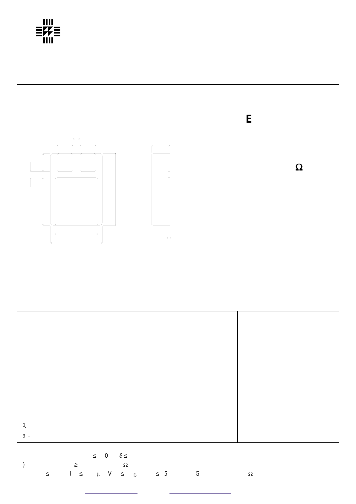
MECHANICAL DATA
Dimensions in mm (inches)
)
)
ABSOLUTE MAXIMUM RATINGS (T
case
= 25°C unless otherwise stated)
SMD1 PACKAGE
Notes
1) Pulse Test: Pulse Width £300ms, d£2%
2) @ VDD= 25V , L ³0.3mH , RG= 25W, Peak IL= 27A , Starting TJ= 25°C
3) @ ISD£
27A , di/dt £70A/ms , VDD£
BV
DSS
, TJ£
150°C , SUGGESTED RG= 2.35
W
N–CHANNEL
POWER MOSFET
FEATURES
• HERMETICALLY SEALED SURFACE
MOUNT PACKAGE
• SMALL FOOTPRINT – EFFICIENT USE OF
PCB SPACE.
• SIMPLE DRIVE REQUIREMENTS
• LIGHTWEIGHT
• HIGH PACKING DENSITIES
Pad 1 – Gate Pad 2 – Drain Pad 3 – Source
Note: IRFNxxx also available with
pins 1 and 3 reversed.
V
DSS
100V
I
D(cont)
19A
R
DS(on)
0.070
WW
WW
0.89
(0.035)
min.
3.70 (0.146)
3.41 (0.134)
4.14 (0.163)
3.84 (0.151)
min.
0.76
(0.030)
10.69 (0.421)
10.39 (0.409)
3.70 (0.146)
3.41 (0.134)
13
2
9.67 (0.381)
9.38 (0.369)
11.58 (0.456)
11.28 (0.444)
16.02 (0.631)
15.73 (0.619)
3.60 (0.142)
Max.
0.50 (0.020
0.26 (0.010
IRF150SMD
Prelim. 7/00
LAB
SEME
Semelab plc. Telephone +44(0)1455 556565. Fax +44(0)1455 552612.
E-mail: sales@semelab.co.uk
Website: http://www.semelab.co.uk
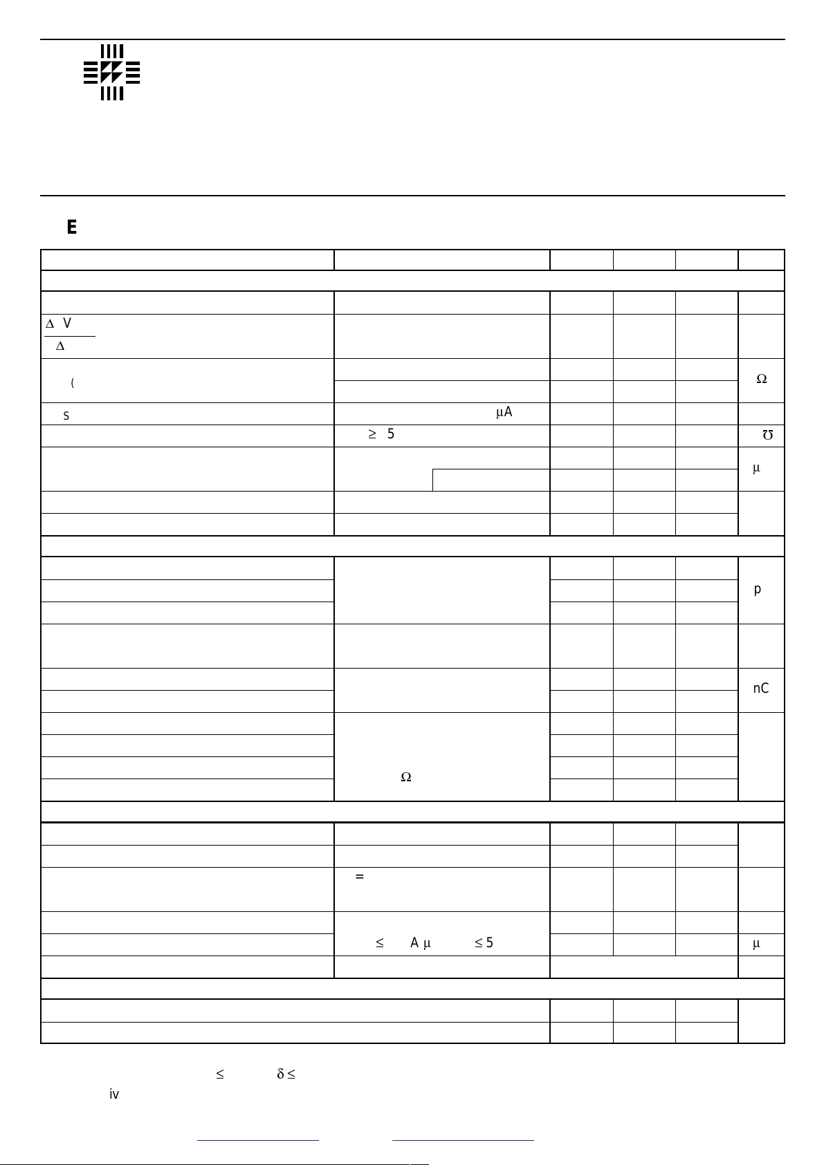
Parameter Test Conditions Min. Typ. Max. Unit
VGS= 0 ID= 1mA
Reference to 25°C
ID= 1mA
VGS= 10V ID= 19A
VGS= 10V ID= 27A
VDS= V
GS
ID= 250mA
VDS³
15V IDS= 19A
VGS= 0 VDS= 0.8BV
DSS
TJ= 125°C
VGS= 20V
VGS= –20V
VGS= 0
VDS= 25V
f = 1MHz
VGS= 10V ID= 27A
VDS= 0.5BV
DSS
ID= 27A
VDS= 0.5BV
DSS
VDD= 50V
I
D
= 27A
RG= 2.35
W
IS= 27A TJ= 25°C
V
GS
= 0
I
F
= 27A TJ= 25°C
di/ dt£
100A/msVDD£
50V
ELECTRICAL CHARACTERISTICS (T
amb
= 25°C unless otherwise stated)
Drain – Source Breakdown Voltage
Temperature Coefficient of
Breakdown Voltage
Static Drain – Source On–State
Resistance
1
Gate Threshold Voltage
Forward Transconductance
1
Zero Gate Voltage Drain Current
Forward Gate
– Source Leakage
Reverse Gate
– Source Leakage
Input Capacitance
Output Capacitance
Reverse Transfer Capacitance
Total Gate Charge
1
Gate – Source Charge
1
Gate – Drain (“Miller”) Charge
1
Turn–On Delay Time
Rise Time
Turn–Off Delay Time
Fall Time
Continuous Source Current
Pulse Source Current
2
Diode Forward Voltage
Reverse Recovery Time
Reverse Recovery Charge
Forward Turn–On Time
100
0.13
0.070
0.081
24
9
25
250
100
–100
3700
1100
200
50 125
822
15 65
35
190
170
130
27
108
1.8
500
2.9
Negligible
0.8
2.8
V
V/°C
W
V
S(
W
m
A
nA
pF
nC
nC
ns
A
V
ns
m
C
nH
BV
DSS
D
BV
DSS
D
T
J
R
DS(on)
V
GS(th)
g
fs
I
DSS
I
GSS
I
GSS
C
iss
C
oss
C
rss
Q
g
Q
gs
Q
gd
t
d(on)
t
r
t
d(off)
t
f
I
S
I
SM
V
SD
t
rr
Q
rr
t
on
L
D
L
S
STATIC ELECTRICAL RATINGS
Notes
1) Pulse Test: Pulse Width £300ms, d£2%
2) Repetitive Rating – Pulse width limited by maximum junction temperature.
DYNAMIC CHARACTERISTICS
SOURCE – DRAIN DIODE CHARACTERISTICS
Internal Drain Inductance
(from centre of drain pad to die)
Internal Source Inductance (from centre of source pad to end of source bond wire)
PACKAGE CHARACTERISTICS
(W)
 Loading...