

Semelab Plc IRF130 Datasheet
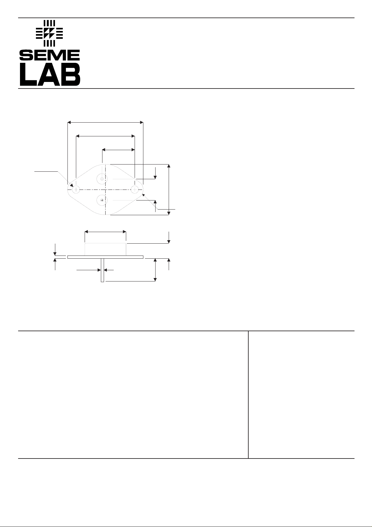
MECHANICAL DATA
Dimensions in mm (inches)
39.95 (1.573)
max.
30.40 (1.197)
30.15 (1.187)
17.15 (0.675)
16.64 (0.655)
IRF130
N–CHANNEL
POWER MOSFET
V
DSS
100V
4.09 (0.161)
3.84 (0.151)
dia.
2 plcs.
1.78 (0.070)
1.52 (0.060)
1.09 (0.043)
0.97 (0.038)
dia.
2 plcs.
20.32 (0.800)
18.80 (0.740)
dia.
2
1
11.18 (0.440)
TO–3 Metal Package
Pin 1 – Gate Pin 2 – Source Case – Drain
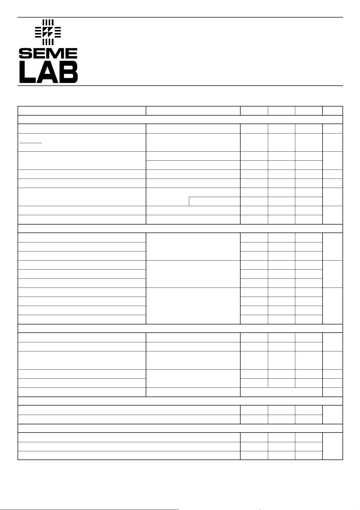
ABSOLUTE MAXIMUM RATINGS (T
V
GS
I
D
I
D
I
DM
P
D
E
AS
I
AR
E
AR
dv/dt Peak Diode Recovery
TJ, T
stg
T
L
Gate – Source Voltage
Continuous Drain Current (VGS= 0 , T
Continuous Drain Current (VGS= 0 , T
Pulsed Drain Current
Power Dissipation @ T
1
case
= 25°C
Linear Derating Factor
Single Pulse Avalanche Energy
Avalanche Current
Repetitive Avalanche Energy
2
2
3
Operating and Storage Temperature Range
Lead Temperature 1.6mm (0.63”) from case for 10 sec.
max.
26.67 (1.050)
10.67 (0.420)
12.07 (0.475)
11.30 (0.445)
case
2
I
D(cont)
R
DS(on)
FEATURES
• HERMETICALLY SEALED TO–3 METAL
PACKAGE
• SIMPLE DRIVE REQUIREMENTS
• SCREENING OPTIONS AVAILABLE
7.87 (0.310)
6.99 (0.275)
= 25°C unless otherwise stated)
= 25°C)
case
= 100°C)
case
14A
0.18
0.6W/°C
5.5V/ns
-55 to +150°C
ΩΩ
±20V
14A
9A
56A
75W
75mJ
14A
7.5mJ
300°C
Notes
1) Pulse Test: Pulse Width ≤ 300µs, δ≤2%
2) @ VDD= 50V , L ≥ 570µH , RG= 25Ω , Peak IL= 14A , Starting TJ= 25°C
3) @ ISD≤ 14A , di/dt ≤ 140A/µs , VDD≤ BV
, TJ≤ 150°C , Suggested RG= 7.5Ω
DSS
Semelab plc. Telephone (01455) 556565. Telex: 341927. Fax (01455) 552612.
Prelim. 9/96
IRF130
ELECTRICAL CHARACTERISTICS (T
= 25°C unless otherwise stated)
case
Parameter Test Conditions Min. Typ. Max. Unit
STATIC ELECTRICAL RATINGS
BV
∆BV
∆T
R
DS(on)
V
GS(th)
g
fs
I
DSS
I
GSS
I
GSS
Drain – Source Breakdown Voltage
DSS
Temperature Coefficient of
DSS
Breakdown Voltage
J
Static Drain – Source On–State
Resistance
1
Gate Threshold Voltage
Forward Transconductance
Zero Gate Voltage Drain Current
Forward Gate
Reverse Gate
– Source Leakage
– Source Leakage
1
VGS= 0 ID= 1mA
Reference to 25°C
ID= 1mA
VGS= 10V ID= 9A
VGS= 10V ID= 14A
VDS= V
GS
ID= 250mA
VDS≥ 15V IDS= 9A
VGS= 0 VDS= 0.8BV
TJ= 125°C
VGS= 20V
VGS= –20V
DYNAMIC CHARACTERISTICS
C
iss
C
oss
C
rss
Q
g
Q
gs
Q
gd
t
d(on)
t
r
t
d(off)
t
f
Input Capacitance
Output Capacitance
Reverse Transfer Capacitance
Total Gate Charge
Gate – Source Charge
Gate – Drain (“Miller”) Charge
Turn–On Delay Time
Rise Time
Turn–Off Delay Time
Fall Time
VGS= 0
VDS= 25V
f = 1MHz
VGS= 10V
ID= 14A
VDS= 0.5BV
VDD= 50V
ID= 14A
RG= 7.5Ω
DSS
SOURCE – DRAIN DIODE CHARACTERISTICS
I
I
V
t
Q
t
S
SM
SD
rr
rr
on
Continuous Source Current
Pulse Source Current
Diode Forward Voltage
2
1
Reverse Recovery Time
Reverse Recovery Charge
Forward Turn–On Time
IS= 14A TJ= 25°C
VGS= 0
IF= 14A TJ= 25°C
1
di/ dt≤ 100A/µsVDD≤ 50V
PACKAGE CHARACTERISTICS
L
D
L
S
Internal Drain Inductance (measured from 6mm down drain lead to centre of die)
Internal Source Inductance (from 6mm down source lead to source bond pad)
THERMAL CHARACTERISTICS
R
R
R
θJC
θCS
θJA
Thermal Resistance Junction – Case
Thermal Resistance Case – Sink
Thermal Resistance Junction – Ambient
Notes
1) Pulse Test: Pulse Width ≤ 300ms, δ≤2%
2) Repetitive Rating – Pulse width limited by maximum junction temperature.
Semelab plc. Telephone (01455) 556565. Telex: 341927. Fax (01455) 552612.
DSS
100
0.13
0.18
0.21
24
4.6
25
250
100
–100
V
V/°C
Ω
V
S (É)
µA
nA
650
250
pF
44
12 35
2.5 10
nC
5.0 15
35
80
60
ns
45
14
56
1.5
300
3.0
A
V
ns
µC
Negligible
5.0
13
nH
1.67
0.12
°C/W
30
Prelim. 9/96
 Loading...