

Semelab Plc IP5561J-883B, IP5561J, IP5561CJ, IP5561CD Datasheet
LAB
SEME
IP5661C
IP5561C
Semelab plc. Telephone (01455) 556565. Telex: 341927. Fax (01455) 552612.
Prelim. 4/95
SWITCHED–MODE
POWER SUPPLY
CONTROL CIRCUIT
FEATURES
• STABILISED POWER SUPPLY
• TEMPERATURE COMPENSATED REFERENCE
SOURCE
• SAWTOOTH GENERATOR
• PULSE WIDTH MODULATOR
• CURRENT LIMITING
• 8 PIN DIP
SUPPLY
Voltage Sourced
Current Sourced
OUTPUT TRANSISTOR
Output Current
Collector Voltage (Pin 7)
T
J
Operating Junction Temperature
T
STG
Storage Temperature Range
18V
30mA
40mA
18V
See Ordering Information
–55 to +150°C
ABSOLUTE MAXIMUM RATINGS (T
case
= 25°C unless otherwise stated)
TOP VIEW
J Package – 8 Pin Ceramic DIP
N Package – 8 Pin Plastic DIP
D Package – 8 Pin Plastic (150) SOIC
1
2
3
4
8
7
6
5
OUTPUT
FEEDBACK
GAIN
GND
CURRENT
SENSE
V
Z
V
CC
RT/C
T
Part J–Pack N–Pack D–8 Temp.
Number 8 Pin 8 Pin 8 Pin Range
IP5561 ✔ -55 to +125°C
IP5561C ✔✔✔0 to +70°C
Order Information
Note:
To order, add the package identifier to the part number.
eg. IP5561J
IP5561CD–8
GAIN
5
SAWTOOTH
GENERATOR
LATCH
S
R
0.5V
CURRENT
SENSE
6
STABILISED
SUPPLY
18
GND
2
4
3
CC
V
z
V
FEEDBACK
ERROR
AMP
PWM
TCT
R
REFERENCE
VOLTAGE
CC
V
OUTPUT
7
8.2V
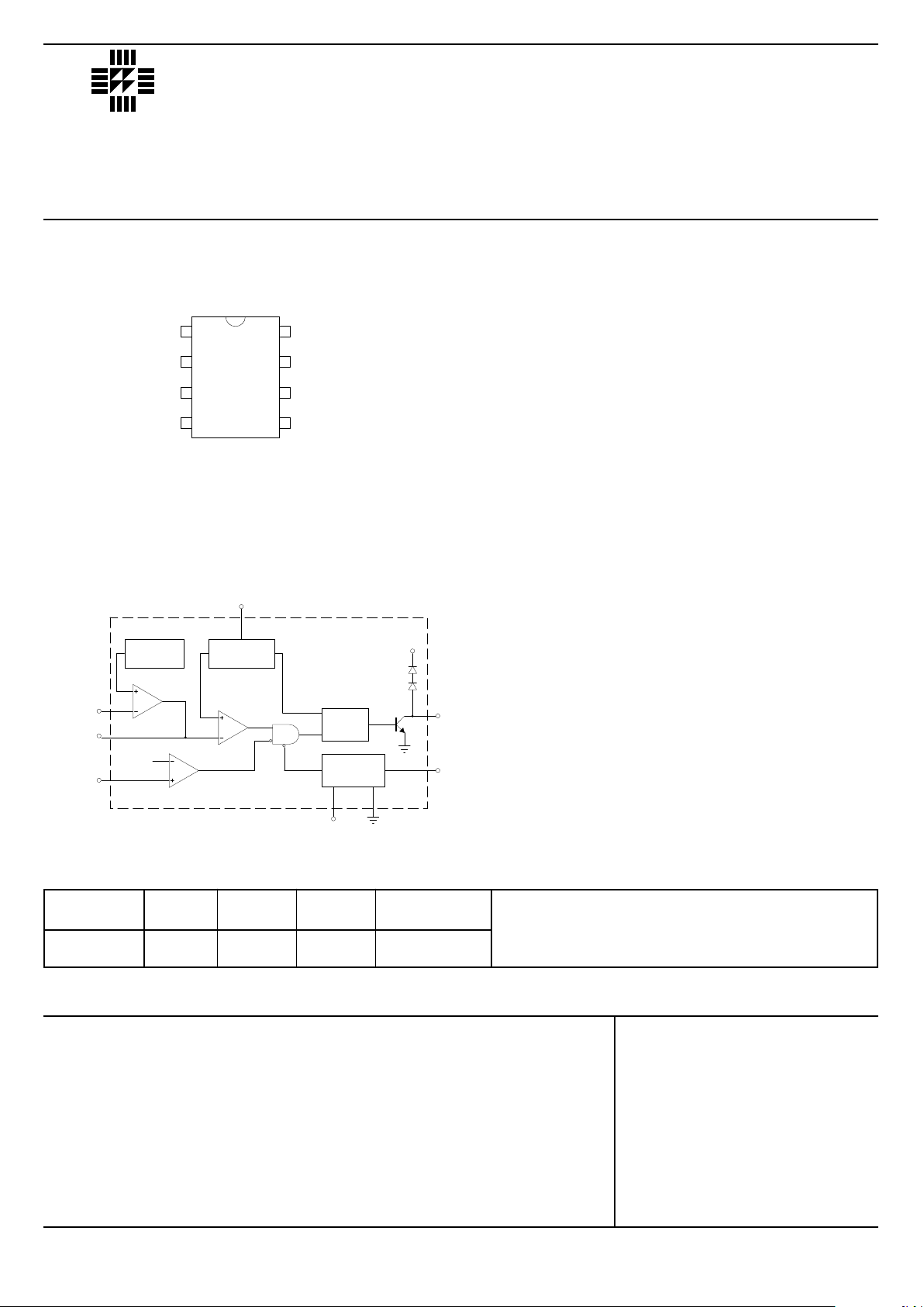
BLOCK DIAGRAM
DESCRIPTION
The IP5561 is a control circuit for use in switched
mode power supplies. This single monolithic chip
incorporates all the control and supervisor y (protection)
functions required in switched mode power supplies,
including an internal temperature compensated
reference source, internal zener reference, sawtooth
generator, pulse width modulator, output stage and
cycle by cycle current limit.

Internal Reference Voltage (V
REF
)
Temperature Coefficient of V
REF
Internal Reference (VZ)
Temperature Coefficient of V
Z
Frequency Range
Initial Accuracy Oscillator
Duty Cycle Range
I
IN
Single Pulse Inhibit Delay
Current Limit Trip Level
Output Voltage Swing (V
OH
)
Output Voltage Swing (V
OL
)
Open Loop Gain
Feedback Resistor
Small Signal Bandwidth
V
CE(sat)
Output Current
Supply Current (I
CC
)
Supply Voltage (V
CC
)
Pin 1 Threshold
T
J
= Over Temp. Range
I
L
= -7mA
T
J
= Over Temp. Range
f
O
= 20kHz
V
pin6
= 250mV
T
J
= Over Temp. Range
Inhibit Delay Time I
OUT
= 20mA
for 20% overdrive I
OUT
= 40mA
IC= 20mA TJ= Over Temp. Range
T
J
= Over Temp. Range
I
Z
= 0, Voltage Fed
T
J
= Over Temp. Range
I
CC
= 10mA, Voltage Fed
I
CC
= 30mA, Voltage Fed
3.69 3.75 3.84
3.65 3.88
±100
7.8 8.2 8.8
±200
50 100k
12
0–90 0–98
–2 –10
-20
0.88 1.10
0.7 0.8
0.40 0.50 0.60
6.2
0.7
60
10k
3
0.4
20
10
13
20 21 22
20 30
8 9 10.5
LAB
SEME
IP5661C
IP5561C
Semelab plc. Telephone (01455) 556565. Telex: 341927. Fax (01455) 552612.
Prelim. 4/95
V
ppm/°C
V
ppm/°C
Hz
%
µA
µs
V
V
dB
Ω
MHz
V
mA
mA
V
V
3.57 3.75 3.96
3.55 3.98
±100
7.8 8.2 8.8
±200
50 100k
12
0–90 0–98
–2 –10
-20
0.88 1.10
0.7 0.8
0.40 0.50 0.60
6.2
0.7
60
10k
3
0.4
20
10
13
19 21 24
20 30
8 9 10.5
IP5561 IP5561C
Parameter Test Conditions Min. Typ. Max. Min. Typ. Max. Units
ELECTRICAL CHARACTERISTICS (T
J
= 25°C unless otherwise stated)
CURRENT LIMITING
ERROR AMPLIFIER
REFERENCE SECTIONS
OSCILLATOR SECTION
OUTPUT STAGE
SUPPLY VOLTAGE/CURRENT
NOTES
1) Test Conditions: VCC= 12V , TJ= 25°C unless otherwise stated
2) Tests marked TJ= Over Temp. Range apply over the full temperature range
ie. TJ= -55 to +125°C for IP5561
TJ= 0 to +70°C for IP5561C
LOW SUPPLY PROTECTION
 Loading...