

Semelab Plc IP3845AN, IP3844AN Datasheet
LAB
SEME
IP1844A SERIES
IP1845A SERIES
Semelab plc. Telephone (01455) 556565. Telex: 341927. Fax (01455) 552612.
Prelim. 2/95
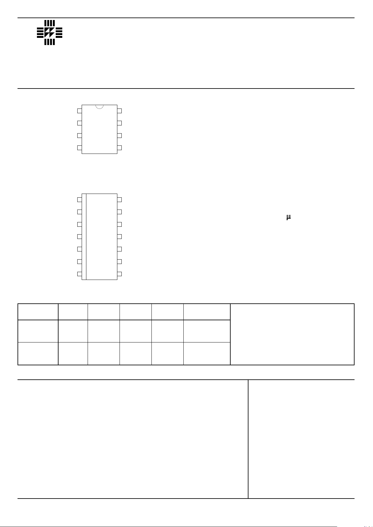
TOP VIEW
J Package – 8 Pin Ceramic DIP
N Package – 8 Pin Plastic DIP
D-8 Package – 8 Pin Plastic (150) SOIC
1
2
3
4
8
7
6
5
COMP
V
REF
GROUND
OUTPUT
RT/C
T
V
CC
I
SENSE
V
FB
TOP VIEW
D-14 Package – 14 Pin Plastic (150) SOIC
COMP
V
REF
GROUND
OUTPUT
1
2
3
4
POWER
GROUND
5
6
7
14
13
12
11
10
9
8
N/C
R
T/CT
I
SENSE
N/C
N/C N/C
V
CC
V
FB
V
C
CURRENT MODE
REGULATING
PULSE WIDTH
MODULATORS
FEATURES
• Guaranteed ±1% reference voltage tolerance
• Accurate oscillator discharge current
• Guaranteed ±10% frequency tolerance
• Low start–up current (<500 mA)
• Under voltage lockout with hysteresis
• Output state completely defined for all supply
and input conditions
• Interchangeable with IP and UC1844/5 series for
improved operation
• 500kHz Oscillator operation
250kHz Output operation
+30V
Self limiting
±1A
5µJ
–0.3V to +V
CC
10mA
1W
10mW/°C
725mW
7.25mW/°C
2W
16mW/°C
–65 to 150°C
+300°C
ABSOLUTE MAXIMUM RATINGS (T
case
= 25°C unless otherwise stated)
V
CC
Supply Voltage (low impedance source)
(ICC< 30mA)
I
O
Output Current
Output Energy (capacitive load)
Analog Inputs (pins 2 and 3)
Error Amp Output Sink Current
P
D
Power Dissipation T
amb
= 25°C J, N Packages
Derate @ T
amb
> 50°C
P
D
Power Dissipation T
case
= 25°C D Package
Derate @ T
amb
> 50°C
P
D
Power Dissipation T
case
= 25°C J, N Packages
Derate @ T
case
> 25°C
T
STG
Storage Temperature Range
T
L
Lead Temperature (soldering, 10 seconds)
Part J–Pack N–Pack D–8 D–14 Temp.
Number 8 Pin 8 Pin 8 Pin 14 Pin Range
IP1844A ✔ -55 to +125°C
IP2844A ✔✔✔✔-25 to +85°C
IP3844A ✔✔✔✔0 to +70°C
IP1845A ✔ -55 to +125°C
IP2845A ✔✔✔✔-25 to +85°C
IP3845A ✔✔✔✔0 to +70°C
Order Information
Note:
To order, add the package identifier to the
part number.
eg. IP1844AD–14
IP3845AJ
LAB
SEME
IP1844A SERIES
IP1845A SERIES
Semelab plc. Telephone (01455) 556565. Telex: 341927. Fax (01455) 552612.
Prelim. 2/95
V
CC
Supply Voltage
1
I
O
Output Current
Analog Inputs (pins 2 and 3)
Error Amp Output Sink Current
IP1844A , IP1845A
Operating Ambient Temperature Range IP2844A , IP2845A
IP3844A , IP3845A
≤ 30V
0 to ±200mA
–0.3V to 3V
0 to 2mA
–55 to 125°C
–25 to 85°C
0 to 70°C
Notes:
1. Lower limit set by under voltage lockout specification.
RECOMMENDED OPERATING CONDITIONS
* 1844A and 1845A series only.
Values in brackets are for IP1845 series.
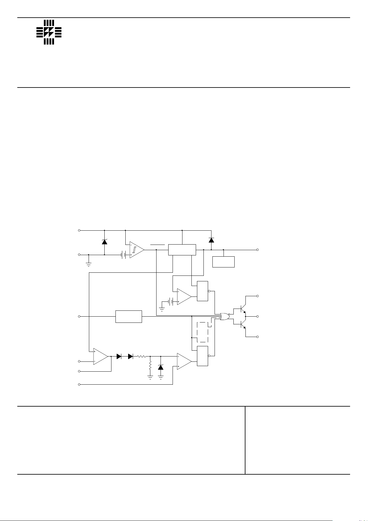
3.6V
ERROR
AMP
OSCILLATOR
2R
R
1V
R
S
PWM
LATCH
CURRENT
SENSE
COMPARATOR
16V
(8.4V)
6V
(0.5V) 2.5V
UNDER–VOLTAGE
LOCKOUT
ENABLE
REFERENCE
REGULATOR
5V
INTERNAL
BIAS
34V
REG
R
S
V STATUS
LATCH
REF
PIN NUMBERS
1st Number
2nd Number
– N, J and 8 Pin D Packag es
– 14 Pin D Package.
C
OMP
G
ND
V
CC
I
SENSE
V
FB
/CR
TT
OUTPUT
POWER
GROUND
V
REF
V
C
3/5
5/9
7/12
2/3
1/1
4/7 6/10
7/11
5/8
8/14
TOGGLE
FLIP
FLOP *
T
Q
DESCRIPTION
The IP1844A/IP1845A series of switching regulator control circuits contain all the functions necessary to
implement off-line, current mode switching regulators, using a minimum number of external parts. Functions
included are voltage reference, error amplifier, current sense comparator, oscillator, totem-pole output driver and
under-voltage lockout circuitry.
In addition the IP1844A and IP1845A series of devices have a toggle flip-flop which blanks the output on every
second clock pulse, thereby ensuring that the duty cycle never exceeds 50%. For applications requiring more
flexible control, all devices feature an on-chip trimmed oscillator discharge current, allowing accurate control to
maximum-duty-cycle by selection of timing components. This can be beneficial even when using the IP1844A or
IP1845A series, as it allows optimum safety margins to be designed into the application.
Although pin compatible with the standard IP1844/5 parts these devices offer improved performance in several
areas. They also offer tighter specification and improved performance over the IP and UC1844/5 series, whilst
retaining complete compatibility.
BLOCK DIAGRAM
 Loading...