

Semelab Plc IP3842D, IP3842AN-200, IP3842AN, IP3842AD-8, IP3842AD-14 Datasheet
V
CC
Supply Voltage (low impedance source)
(ICC< 30mA)
I
O
Output Current
Output Energy (capacitive load)
Analog Inputs (pins 2 and 3)
Error Amp Output Sink Current
P
D
Power Dissipation T
amb
= 25°C J, N Packages
Derate @ T
amb
> 50°C
P
D
Power Dissipation T
case
= 25°C D Package
Derate @ T
amb
> 50°C
P
D
Power Dissipation T
case
= 25°C J, N Packages
Derate @ T
case
> 25°C
T
STG
Storage Temperature Range
T
L
Lead Temperature (soldering, 10 seconds)
+30V
Self limiting
±1A
5µJ
–0.3V to +V
CC
10mA
1W
10mW/°C
725mW
7.25mW/°C
2W
16mW/°C
–65 to 150°C
+300°C
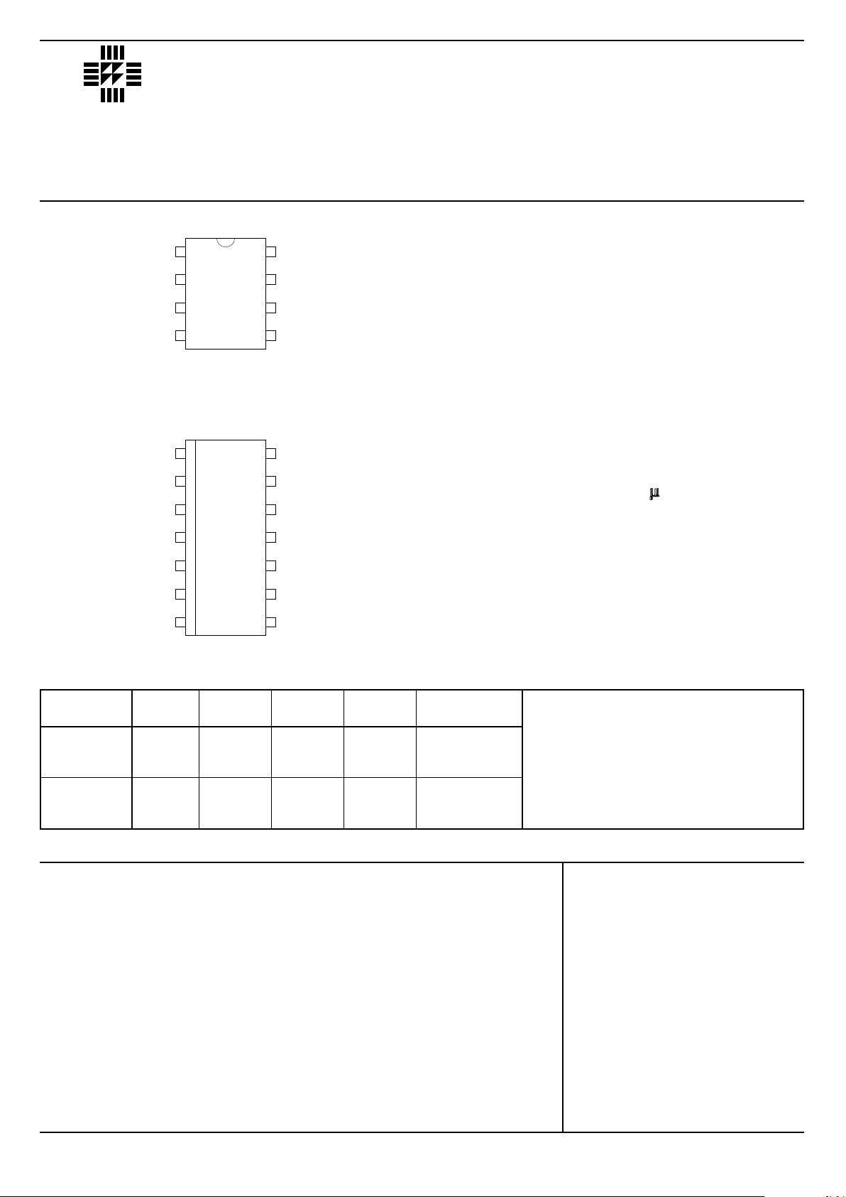
TOP VIEW
J Package – 8 Pin Ceramic DIP
N Package – 8 Pin Plastic DIP
D-8 Package – 8 Pin Plastic (150) SOIC
1
2
3
4
8
7
6
5
COMP
V
REF
GROUND
OUTPUT
RT/C
T
V
CC
I
SENSE
V
FB
TOP VIEW
D-14 Package – 14 Pin Plastic (150) SOIC
COMP
V
REF
GROUND
OUTPUT
1
2
3
4
POWER
GROUND
5
6
7
14
13
12
11
10
9
8
N/C
R
T/CT
I
SENSE
N/C
N/C N/C
V
CC
V
FB
V
C
ABSOLUTE MAXIMUM RATINGS (T
case
= 25°C unless otherwise stated)
LAB
SEME
IP1842A SERIES
IP1843A SERIES
Semelab plc. Telephone (01455) 556565. Telex: 341927. Fax (01455) 552612.
Prelim. 2/95
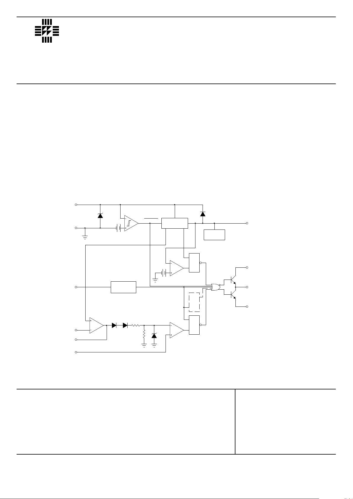
CURRENT MODE
REGULATING
PULSE WIDTH
MODULATORS
FEATURES
• Guaranteed ±1% reference voltage tolerance
• Accurate oscillator discharge current
• Guaranteed ±10% frequency tolerance
• Low start–up current (<500 mA)
• Under voltage lockout with hysteresis
• Output state completely defined for all supply
and input conditions
• Interchangeable with IP and UC1842/3 series for
improved operation
• 500kHz Oscillator operation
Part J–Pack N–Pack D–8 D–14 Temp.
Number 8 Pin 8 Pin 8 Pin 14 Pin Range
IP1842A ✔ -55 to +125°C
IP2842A ✔✔✔✔-25 to +85°C
IP3842A ✔✔✔✔0 to +70°C
IP1843A ✔ -55 to +125°C
IP2843A ✔✔✔✔-25 to +85°C
IP3843A ✔✔✔✔0 to +70°C
Order Information
Note:
To order, add the package identifier to the
part number.
eg. IP1842AD–14
IP3843AJ
* 1844A and 1845A series only.
Values in brackets are for IP1845 series.
3.6V
ERROR
AMP
OSCILLATOR
2R
R
1V
R
S
PWM
LATCH
CURRENT
SENSE
COMPARATOR
16V
(8.4V)
6V
(0.5V) 2.5V
UNDER–VOLTAGE
LOCKOUT
ENABLE
REFERENCE
REGULATOR
5V
INTERNAL
BIAS
34V
REG
R
S
V STATUS
LATCH
REF
PIN NUMBERS
1st Number
2nd Number
– N, J and 8 Pin D Packag es
– 14 Pin D Package.
C
OMP
G
ND
V
CC
I
SENSE
V
FB
/CR
TT
OUTPUT
POWER
GROUND
V
REF
V
C
3/5
5/9
7/12
2/3
1/1
4/7 6/10
7/11
5/8
8/14
TOGGLE
FLIP
FLOP *
T
Q
LAB
SEME
IP1842A SERIES
IP1843A SERIES
Semelab plc. Telephone (01455) 556565. Telex: 341927. Fax (01455) 552612.
Prelim. 2/95
V
CC
Supply Voltage
1
I
O
Output Current
Analog Inputs (pins 2 and 3)
Error Amp Output Sink Current
IP1842A , IP1843A
Operating Ambient Temperature Range IP2842A , IP2843A
IP3842A , IP3843A
≤ 30V
0 to ±200mA
–0.3V to 3V
0 to 2mA
–55 to 125°C
–25 to 85°C
0 to 70°C
Notes:
1. Lower limit set by under voltage lockout specification.
DESCRIPTION
The IP1842A/IP1843A series of switching regulator control circuits contain all the functions necessary to
implement off-line, current mode switching regulators, using a minimum number of external parts. Functions
included are voltage reference, error amplifier, current sense comparator, oscillator, totem-pole output driver and
under-voltage lockout circuitry.
Although pin compatible with the standard IP1842/3 parts these devices offer improved performance in several
areas. They also offer tighter specification and improved performance over the IP and UC1842/3 series, whilst
retaining complete compatibility.
BLOCK DIAGRAM
RECOMMENDED OPERATING CONDITIONS
 Loading...