

Semelab Plc IP33063N, IP33063J, IP35063J-BSS2, IP35063J-883B, IP34063J Datasheet
...
IP35063
IP33063
IP34063
Semelab plc. Telephone (01455) 556565. Telex: 341927. Fax (01455) 552612.
Prelim. 2/95
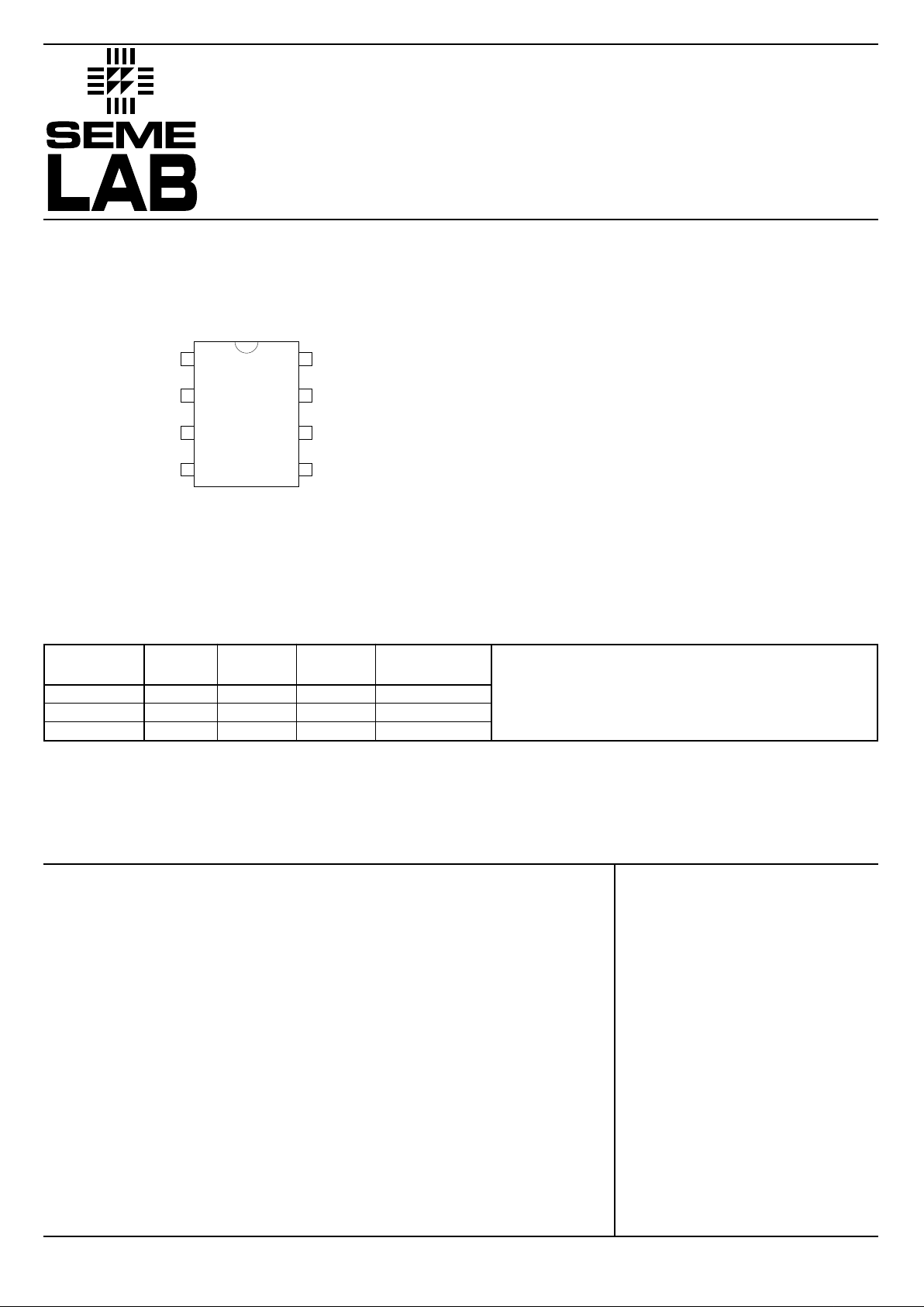
TOP VIEW
J Package – 8 Pin Ceramic DIP
N Package – 8 Pin Plastic DIP
D-8 Package – 8 Pin Plastic (150) SOIC
Part J–Pack N–Pack D–8 Temp.
Number 8 Pin 8 Pin 8 Pin Range
IP35063 ✔ -55 to +125°C
IP33063 ✔✔✔-40 to +85°C
IP34063 ✔✔✔0 to +70°C
FEATURES
• Operation from 2.5 to 40V input
• Low Standby Current
• Current Limiting
• Output switch current of 1.5A
• Output voltage adjustable from 1.25 to 40V
• Operating frequency from 100Hz to 100kHz
• Direct replacement for MC34063/MC34063A
series
Power Supply Voltage
Comparator Input Voltage Range
Switch Collector Voltage
Switch Emitter Voltage
Switch Collector to Emitter Voltage
Driver Collector Voltage
Switch Current
Power Dissipation @ T
amb
= 25°C Ceramic Packages
Plastic Packages
Derate above 25°C
Operating Junction Temperature Ceramic Packages
Plastic Packages
Operating Ambient Temperature Range See Table Above
Storage Temperature Range
+40V
–0.3V to +40V
40V
40V
40V
40V
1.5A
1.25W
1W
10mW/°C
150°C
125°C
See Table Above
–65 to 150°C
ABSOLUTE MAXIMUM RATINGS
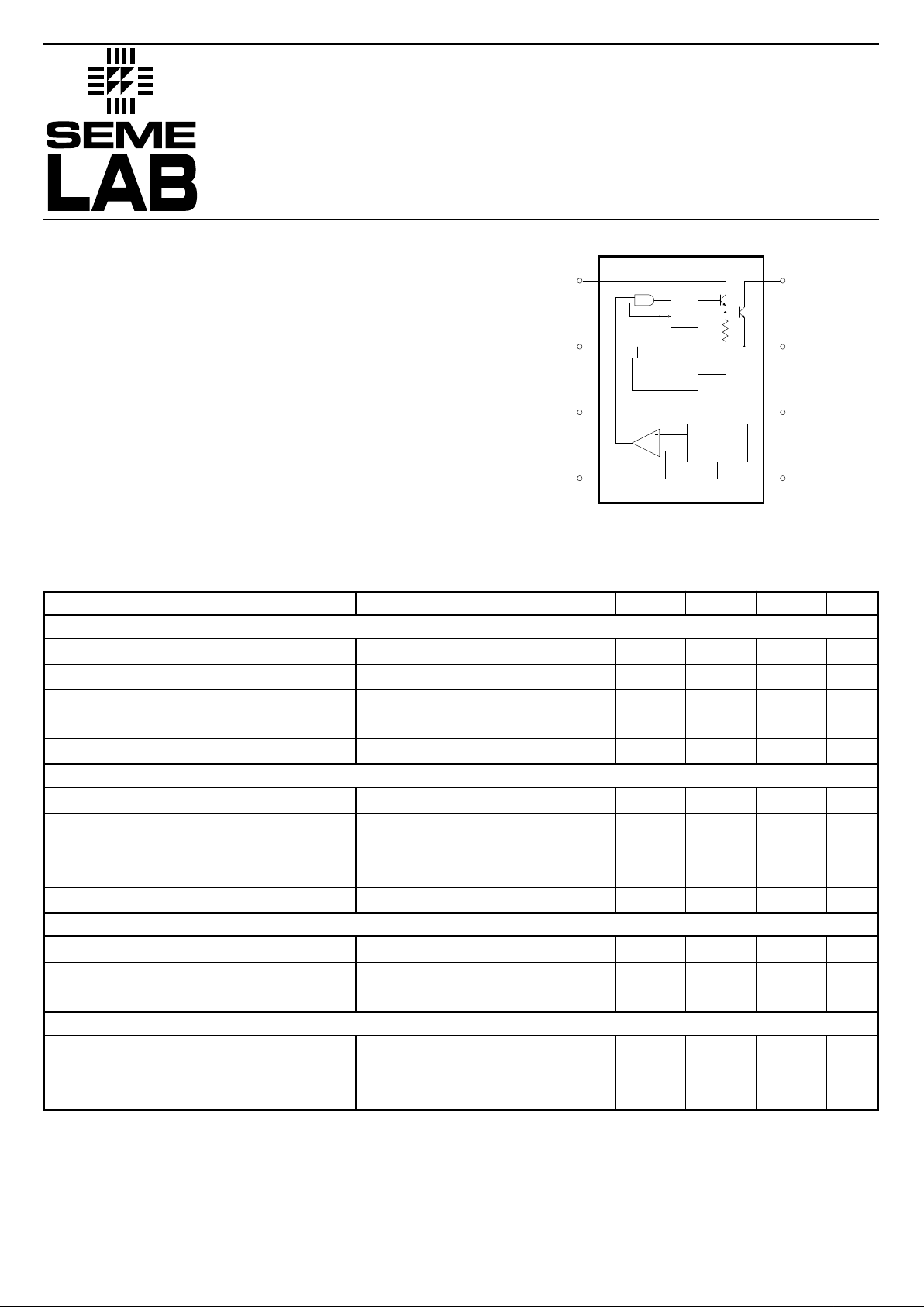
1
2
3
4
8
7
6
5
V
CC
SWITCH
COLLECTOR
SWITCH
EMITTER
TIMING
CAPACITOR
GND
I
pk SENSE
DRIVER
COLLECTOR
CO MPARATOR
INVERTING
INPUT
DC–DC CONVERTER
CONTROL CIRCUIT
Order Information
Note:
To order, add the package identifier to the part
number.
eg. IP35063D–8
IP35063
IP33063
IP34063
Semelab plc. Telephone (01455) 556565. Telex: 341927. Fax (01455) 552612.
Prelim. 2/95
Parameter Test Conditions Min. Typ. Max. Units
20 35 50
150 200 250
0.5
6.0
250 300 350
1 1.3
0.45 0.7
35 120
10
1.18 1.25 1.32
0.04 0.2
40 400
2.4 3.5
Charging Current
Discharge Current
Voltage Swing
Discharge to Charge Current Ratio
Current Limit Sense Voltage
Saturation Voltage, Darlington Connection *
Saturation Voltage *
DC Current Gain
Collector Off–State Current
Threshold Voltage *
Threshold Voltage Line Regulation *
Input Bias Current *
Supply Current *
VCC= 5 to 40V
VCC= 5 to 40V
I
pk(sense)
= V
CC
I
chg
= I
dischg
ISW= 1.0A
ISW= 1.0A
I
C(Driver)
= 50mA (Forced β = 20)
ISW= 1.0A , VCE= 5.0V
VCE= 40V
VCC= 3 to 40V
VIN= 0V
VCC= 5 to 40V CT= 0.001µF
I
pk(sense)
= V
CC
V
PIN 5
> V
th
Pin 2 = Gnd , Remaining Pins Open.
µA
µA
Vpp
—
mV
V
V
—
nA
V
mV/V
nA
mA
ELECTRICAL CHARACTERISTICS (Test Parameters unless otherwise stated : V
CC
= 5V , TJ= 25°C)
OUTPUT SWITCH
COMPARATOR
TOTAL DEVICE
OSCILLATOR
NOTES
* Applies over full operating temperature range (see order information).
1.25 V
REFERENCE
REGULATOR
COMPARATOR
OSCILLATOR
SRQ
8
7
6
5
1
2
3
4
Q1
Q2
170
Ω
Switch
Collector
Switch
Emitter
Timing
Capacitor
Gnd
Driver
Collector
I Sense
pk
V
CC
Comparator
Inverting
Input
DESCRIPTION
The IP34063 series of control circuits contains all the
functions required to implement DC–DC converters.
Included are internal voltage reference, comparator,
controlled duty cycle oscillator with current limit circuit,
driver, and high current output switch. This series was
specifically designed to be incorporated in Step-Down
(Buck) and Step-Up (Boost) applications with a minimum
number of external components.
 Loading...