

Semelab Plc IP3524BN, IP3524BJ, IP2524BN, IP2524BD, IP1524BJ-BSS2 Datasheet
...
LAB
SEME
IP1524B SERIES
Semelab plc. Telephone (01455) 556565. Telex: 341927. Fax (01455) 552612.
Prelim. 3/95
REGULATING
PULSE WIDTH
MODULATORS
FEATURES
• Pin Compatible with IP1524 Series
• 7 to 40 volt operation
• 5 volt reference trimmed to ±1%
• Undervoltage lockout
• Excellent external sync capability
• Wide current limit common mode range
• +5 Volt error amplifier common mode
• PWM data latch
• Full double-pulse suppression logic
• 50ns shutdown function
• Dual 200mA, 60V output transistors
• Fully specified over temperature
+V
IN
Input Voltage
Collector Voltage
Logic Inputs
Current Limit Sense Inputs
Oscillator Charging Current
P
D
Power Dissipation TA= 25°C
Derate @ TA> 50°C
P
D
Power Dissipation TC= 25°C
Derate @ TC> 25°C
T
J
Operating Junction Temperature
T
STG
Storage Temperature Range
T
L
Lead Temperature (soldering, 10 seconds)
+40V
+60V
–0.3 to +5.5V
–0.3 to +V
IN
5mA
1W
10mW/°C
2W
16mW/°C
See Ordering Information
–65 to +150°C
+300°C
ABSOLUTE MAXIMUM RATINGS (T
case
= 25°C unless otherwise stated)
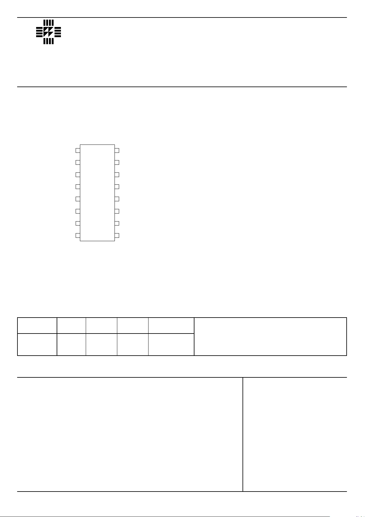
TOP VIEW
J Package – 16 Pin Ceramic DIP
N Package – 16 Pin Plastic DIP
D Package – 16 Pin Plastic (300) SOIC
8
1
2
3
4
5
6
7
14
13
12
11
10
9
15
16
INV. IN P UT
N. I. INPUT
OSC. OUTPUT
+C.L. SENSE
–C.L. SE NSE
R
T
C
T
GROUND
V
REF
V
IN
E
B
C
B
C
A
E
A
SHUTDOWN
COMPENSATION
Part J–Pack N–Pack D–16 Temp.
Number 16 Pin 16 Pin 16 Pin Range
IP1524B ✔ -55 to +125°C
IP2524B ✔✔✔-25 to +85°C
IP3524B ✔✔✔0 to +70°C
Order Information
Note:
To order, add the package identifier to the part number.
eg. IP1524BJ
IP3524BD–16
LAB
SEME
IP1524B SERIES
Semelab plc. Telephone (01455) 556565. Telex: 341927. Fax (01455) 552612.
Prelim. 3/95
E
C
C.L.
+C.L.
SENSE
–C.L.
SENSE
INV.
INPUT
N.I.
INPUT
T
T
6
7
OSCILLATOR
R
C
15
8
REFERENCE
REGULATOR
GND
UNDER
VOLTAGE
LOCKOUT
TO INTERNAL
CIRCUITRY
OSC.
D
S
Q
Q
S
QR Q
T
Q
1
2
5
4
COMPENSATION
SHUTDOWN
9
10
PWM
LATCH
MEMORY
F/F
TOGGLE
F/F
PWM
ERROR
+V
IN
V
REF
16
3
C
E
B
B
A
A
11
12
13
14
+7 to +40V
0 to +60V
+2.3 to V
REF
0 to VIN– 2.5V
0 to 200mA
0 to 20mA
25µA to 1.8mA
50Hz to 500kHz
2kΩ to 150kΩ
1nF to 0.1µF
–55 to +125°C
–25 to +85°C
0 to +70°C
RECOMMENDED OPERATING CONDITIONS
DESCRIPTION
The IP1524B is a pulse width modulator for switching power supplies which features improved performance over
industry standards like the SG1524. A direct pin-for-pin replacement for the earlier device, it combines advanced
processing techniques and circuit design to provide improved reference accuracy/ and extended common mode range at
the error amplifier and current limit inputs. A DC-coupled flip-flop eliminates triggering and glitch problems, and a PWM
data latch prevents edge oscillations. The circuit incorporates true digital shutdown for high speed response, while an
undervoltage lockout circuit prevents spurious outputs when the supply voltage is too low for stable operation. Full
double-pulse suppression logic insures alternating output pulses when the shutdown pin is used for pulse-by-pulse
current limiting.
BLOCK DIAGRAM
V
IN
Input Voltage
Collector Voltage
Error Amp Common Mode Range
Current Limit Sense Common Mode Range
Output Current (each transistor)
Reference Load Current
Oscillator Charging Current
Oscillator Frequency Range
R
T
Oscillator Timing Resistor
C
T
Oscillator Timing Capacitor
Operating Ambient Temperature Range IP1524B
IP2524B
IP3524B
NOTES
1. Test Conditions unless otherwise stated:
V
IN
= 20V , I
REF
= 0.
T
J
= –55 to +125°C for IP1524B
T
J
= –25 to +85°C for IP2524B
T
J
= 0 to +70°C for IP3524B
2. R
T
= 2.7KΩ , CT= 0.01µF unless otherwise stated.
LAB
SEME
IP1524B SERIES
Semelab plc. Telephone (01455) 556565. Telex: 341927. Fax (01455) 552612.
Prelim. 3/95
4.3 5.2 6.5
0.1 0.3 0.6
710
4.90 5.00 5.10
4.85 5.15
115
525
40 75
25 70 120
1
39 43 47
0.1 1
12
80 140
400 700
3.0 4.0
0.4 0.5 1.2
3.7 4.0
0.6 1 1.1
-1
210
110
0.1 1
4.3 5.2 6.5
0.1 0.3 0.6
710
4.95 5.00 5.05
4.90 5.10
110
515
40 75
25 70 120
110
41 43 45
0.1 1
12
80 140
400 700
3.0 4.0
0.4 0.5 1.2
3.7 4.0
0.6 1 1.1
-1
0.1 5
15
0.1 1
IP1524B
IP2524B IP3524B
Parameter Test Conditions
1
Min. Typ. Max. Min. Typ. Max. Units
VINUndervoltage Threshold
Turn–on Hysteresis
Operating Current
Output Voltage
Line Regulation
Load Regulation
Temperature Stability
Short Circuit Current
Long Term Stability
Initial Accuracy
Voltage Stability
Temperature Stability
Minimum Frequency
Maximum Frequency
Clock Amplitude
Clock Pulse Width
Sawtooth Peak Voltage
Sawtooth Valley Voltage
Sawtooth Valley T.C.
Input Offset Voltage
Input Bias Current
Input Offset Current
V
IN
Rising
V
IN
= 7 to 40V
T
J
= 25°C
V
IN
= 7 to 40V IL= 0 to 20mA
V
IN
= 7 to 40V
I
L
= 0 to 20mA
V
REF
= 0
T
J
= 25°C
T
J
= 25°C
V
IN
= 7 to 40V
R
T
= 150kΩ CT= 0.1µF
R
T
= 2kΩ CT= 470pF
Output, Pin 3 C
T
= 0.01µF
Output, Pin 3 C
T
= 0.01µF
C
T
= 0.01µF
C
T
= 0.01µF
T
J
= 25°C
V
CM
= 2.3 to V
REF
VCM= 2.3 to V
REF
VCM= 2.3 to V
REF
V
mA
V
mV
mA
mV
khr
kHz
%
Hz
kHz
V
µs
V
mV/°C
mV
µA
ELECTRICAL CHARACTERISTICS (T
J
= Over Operating Temperature Range unless otherwise stated)
ERROR AMP SECTION
OSCILLATOR SECTION
2
REFERENCE SECTION
TURN–ON CHARACTERISTICS
 Loading...