

Semelab Plc IP117MHVLCC4, IP117MALCC4, IP117MAHVLCC4, IP117MLCC4, IP117LCC4 Datasheet
Semelab plc. Telephone (01455) 556565. Telex: 341927. Fax (01455) 552612.
Prelim. 1/99
IP117MAHV-LCC4
IP117MHV-LCC4
IP117MA-LCC4
IP117M-LCC4A
0.5 AMP
POSITIVE ADJUSTABLE
VOLTAGE REGULATOR
IN CERAMIC SURFACE
MOUNT PACKAGE
V
I–O
Input - Output Differential Voltage – Standard
– HV Series
P
D
Power Dissipation
T
J
Operating Junction Temperature Range
T
STG
Storage Temperature
40V
60V
Internally limited
–55 to 150°C
–65 to 150°C
ABSOLUTE MAXIMUM RATINGS (T
case
= 25°C unless otherwise stated)
FEATURES
• OUTPUT VOLTAGE RANGE ADJUSTABLE:
1.25 TO 40V FOR STANDARD VERSION
1.25 TO 60V FOR –HV VERSION
• 1% OUTPUT VOLTAGE TOLERANCE
(–A VERSIONS)
• 0.3% LOAD REGULATION
• 0.01%/V LINE REGULATION
• COMPLETE SERIES OF PROTECTIONS:
• CURRENT LIMITING
• THERMAL SHUTDOWN
• SOA CONTROL
DESCRIPTION
The IP117M Series are three terminal positive adjustable voltage regulators capable of supplying in excess of 0.5A over a
1.25V to 60V output range. These regulators are exceptionally easy to use and require only two external resistors to set the
output voltage. In addition to improved line and load regulation, a major feature of the “A” series is the initial output voltage
tolerance, which is guaranteed to be less than 1%.
Over full operating conditions, including load, line, and power dissipation, the reference voltage is guaranteed not to vary more
than 2%. These devices exhibit current limit, thermal overload protection, and improved power device safe operating area
protection, making them essentially indestructible.
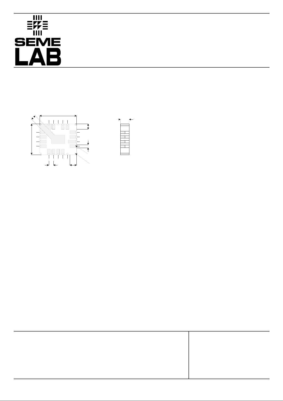
1.39 (0.055)
1.15 (0.045)
0.76 (0.030)
0.51 (0.020)
1.39 (0.055)
1.02 (0.040)
15
16
13
12
14
34
56
7
17
18
1
2
11
10
8
9
9.14 (0.360)
8.64 (0.340)
1.27 (0.050)
1.07 (0.040)
≈2.16 (0.085)
7.62 (0.300)
7.12 (0.280)
1.65 (0.065)
1.40 (0.055)
0.33 (0.013)
0.08 (0.003)
0.43 (0.017)
0.18 (0.007
Rad.
Rad.
Pins 4,5 – Adjust
Pins 6,7,8,9,10,11,12,13 – V
IN
Pins 15,16,17,18,1,2 – V
OUT
Semelab plc. Telephone (01455) 556565. Telex: 341927. Fax (01455) 552612.
Prelim. 1/99
IP117MAHV-LCC4
IP117MHV-LCC4
IP117MA-LCC4
IP117M-LCC4A
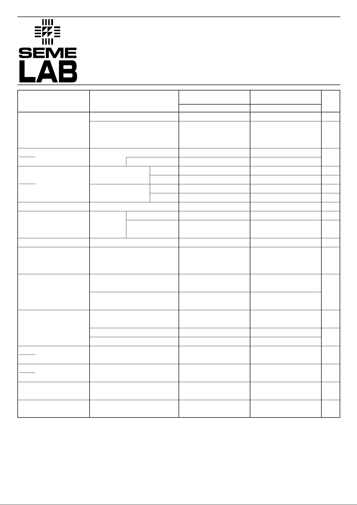
1) Regulation is measured at constant junction temperature, using pulse testing at a low duty cycle. Changes in output voltage due to
heating effects are covered under thermal regulation specifications.
2) Test Conditions unless othewise stated: V
IN
– V
OUT
= 5V , TJ= 25°C , I
OUT
= 0.1A , P
MAX
= 10W , I
MAX
= 0.5A
V
MAX
= 40V for standard series , 60V for HV series.
1.238 1.25 1.262
1.220 1.250 1.270
0.005 0.010
0.010 0.020
515
0.1 0.3
15 50
0.3 1
0.002 0.020
65
66 80
50 100
0.2 5
3.5 5
3.5 7
0.50 0.80
0.15 0.20
0.30
12
0.3 1
0.001
13
1.200 1.250 1.300
0.010 0.020
0.020 0.050
515
0.1 0.3
20 50
0.3 1
0.030 0.070
65
66 80
50 100
0.2 5
3.5 5
3.5 7
0.50 0.80
0.15 0.20
0.30
1
0.3 1
0.001
13
IP117MAHV IP117MHV , IP117M
IP117MA
Parameter Test Conditions Min. Typ. Max. Min. Typ. Max. Units
V
REF
Reference Voltage
∆V
OUT
Line Regulation
1
∆V
IN
∆V
OUT
Load Regulation
1
∆I
OUT
Thermal Regulation
Ripple Rejection
I
ADJ
Adjust Pin Current
∆I
ADJ
Adjust Pin Current
Change
I
MIN
Minimum Load
Current
I
CL
Current Limit
∆V
OUT
Temperature
∆TEMP Stability
∆V
OUT
Long Term Stability
∆TIME
e
n
RMS Output Noise
(% of V
OUT
)
R
θJC
Thermal Resistance
Junction to Case
I
OUT
= 10mA
I
OUT
= 10mA to I
MAX
VIN– V
OUT
= 3V to V
MAX
P ≤ P
MAX
TJ= –55 to +150°C
V
IN
– V
OUT
= 3V to V
MAX
TJ= –55 to +150°C
I
OUT
= 10mA to I
MAX
V
OUT
≤ 5V
V
OUT
≥ 5V
I
OUT
= 10mA to I
MAX
V
OUT
≤ 5V
T
J
= –55 to +150°C V
OUT
≥ 5V
t
p
= 20ms
C
ADJ
= 0
V
OUT
= 10V
C
ADJ
= 10µF
f = 120Hz
T
J
= –55 to +150°C
T
J
= –55 to +150°C
I
OUT
= 10mA to I
MAX
TJ= –55 to +150°C
V
IN
– V
OUT
= 2.5V to V
MAX
VIN– V
OUT
= 40V
T
J
= –55 to +150°C
V
IN
– V
OUT
= 60V (HV SERIES)
TJ= –55 to +150°C
V
IN
– V
OUT
≤ 15V
T
J
= –55 to +150°C
V
IN
– V
OUT
= 40V
V
IN
– V
OUT
= 60V (HV SERIES)
TJ= –55 to +150°C
T
A
= +125°C t = 1000 Hrs
f = 10 Hz to 10 kHz
LCC4 Package
V
V
% / V
mV
%
mV
%
%/W
dB
dB
µA
µA
mA
A
A
%
%
%
°C/W
 Loading...