

SEME LAB 2N7091 Technical data
2N7091
Document Number 2653
Issue 1
Semelab plc. Telephone +44(0)1455 556565. Fax +44(0)1455 552612.
E-mail: sales@semelab.co.uk
Website: http://www.semelab.co.uk
Semelab Plc reserves the right to change test conditions, parameter limits and package dimensions without notice. Information furnished by Semelab is believed
to be both accurate and reliable at the time of going to press. However Semelab assumes no responsibility for any errors or omissions discovered in its use.
Semelab encourages customers to verify that datasheets are current before placing orders.
V
DS
Drain – Source Voltage
V
GS
Gate – Source Voltage
I
D
Continuous Drain Current (TJ= 150°C) TC= 25°C
T
C
= 100°C
I
DM
Pulsed Drain Current
P
D
Power Dissipation TC= 25°C
T
C
= 100°C
T
J
, T
stg
Operating Junction and Storage Temperature Range
T
L
Lead Temperature (
1
/
16
” from case for 10 sec.)
- 100V
±20V
-14A
-8.7A
56A
70W
27W
–55 to 150°C
300°C
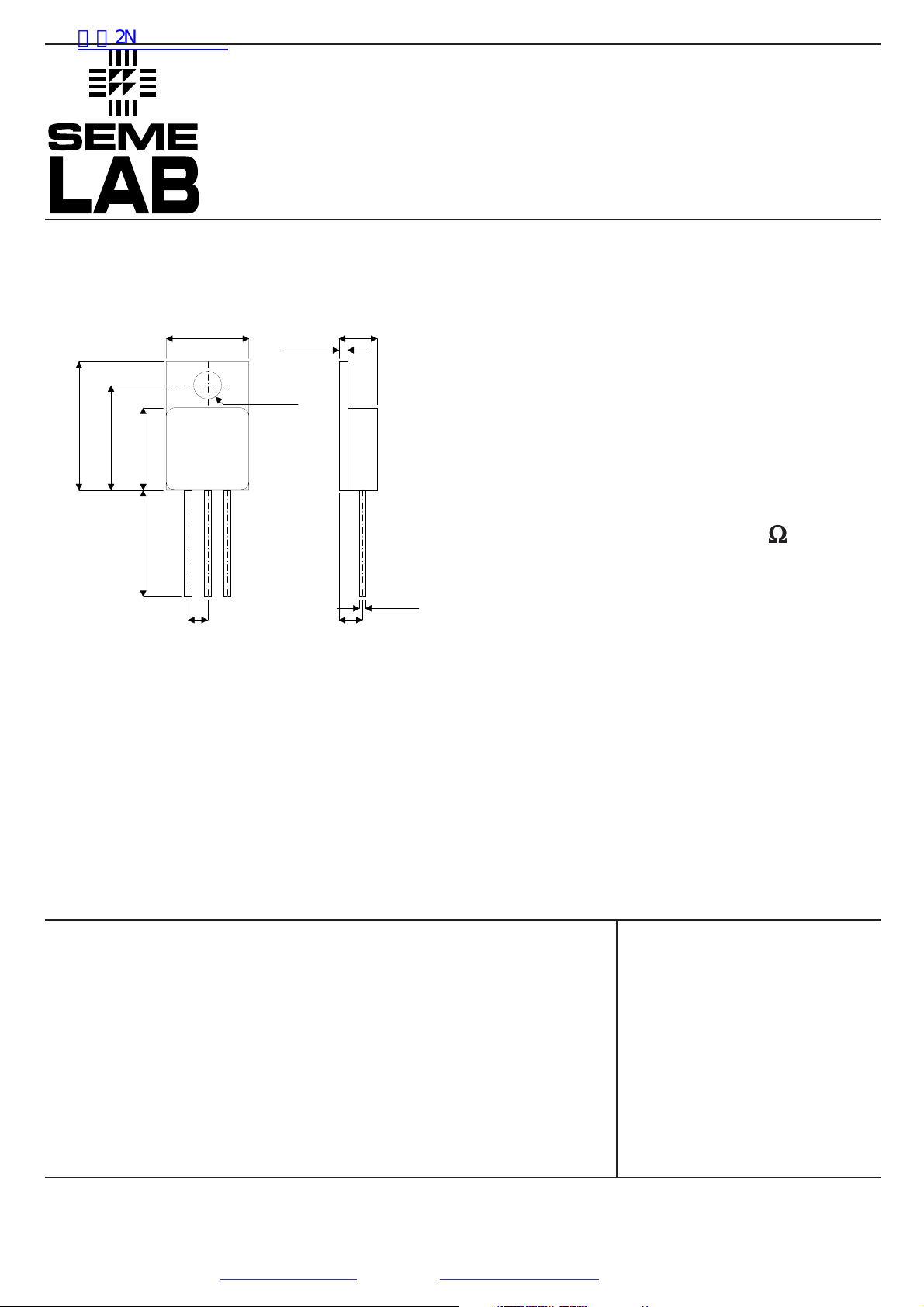
MECHANICAL DATA
Dimensions in mm(inches)
ABSOLUTE MAXIMUM RATINGS (T
case
= 25°C unless otherwise stated)
TO–257AB Metal Package
P–CHANNEL
ENHANCEMENT MODE
TRANSISTOR
FEATURES
• TO257AB HERMETIC PACKAGE FOR
HIGH RELIABILITY APPLICATIONS
• SCREENING OPTIONS AVAILBLE
• SIMPLE DRIVE REQUIREMENTS
Pin 1 – Gate Pin 2 – Drain Pin 3 – Source
V
(BR)DSS
-100V
I
D(A)
-14A
R
DS(on)
0.20
WW
WW
查询2N7091供应商
4.83 (0.190)
5.08 (0.200)
Dia.
16.38 (0.645)
16.89 (0.665)
10.4 1 (0 .410 )
10.6 7 (0 .420 )
13.38 (0.527)
13.64 (0.537)
10.41 (0.410)
10.92 (0.430)
3.56 (0.140)
3.81 (0.150)
0.89 (0.035)
1.14 (0.045)
123
12.07 (0.500)
19.05 (0.750)
2.54 (0.100)
BSC
3.05 (0.120)
BSC
0.64 (0.025)
0.89 (0.035)
Dia.
Parameter Min. Typ. Max. Unit
R
thJC
Thermal resistance Junction-Case 1.8
R
thJA
Thermal resistance Junction-ambient 80
°C/W
R
thCS
Thermal resistance Case to Sink 1.0
2N7091
Document Number 2653
Issue 1
Semelab plc. Telephone +44(0)1455 556565. Fax +44(0)1455 552612.
E-mail: sales@semelab.co.uk
Website: http://www.semelab.co.uk
Semelab Plc reserves the right to change test conditions, parameter limits and package dimensions without notice. Information furnished by Semelab is believed
to be both accurate and reliable at the time of going to press. However Semelab assumes no responsibility for any errors or omissions discovered in its use.
Semelab encourages customers to verify that datasheets are current before placing orders.
Parameter Test Conditions Min. Typ. Max. Unit
VGS= 0 ID= -250µA
VDS= V
GS
ID= -250µA
VDS= 0 VGS= ±20V
VDS= -80V
VGS= 0 TJ= 125°C
VDS= -10V VGS= -10V
VGS= -10V
ID= 8.7A TJ= 125°C
VDS= -15V IDS= -8.7A
VGS= 0
VDS= 25V
f = 1MHz
VDS= -50
VGS= -10V ID= -14A
VDD= -50V ID= -14A
V
GEN
=-10V
RL= 3.5
W
RG= 4.7
W
IF= -14A VGS= 0
I
F
= -14A
di/dt = 100A/µs
ELECTRICAL CHARACTERISTICS (T
J
= 25°C unless otherwise stated)
THERMAL RESISTANCECHARACTERISTICS
Drain–Source Breakdown Voltage
Gate Threshold Voltage
Gate – Body Leakage
Zero Gate Voltage Drain Current
On–State Drain Current
1
Drain – Source On–State
Resistance
1
Forward Transconductance
1
Input Capacitance
Output Capacitance
Reverse Transfer Capacitance
Total Gate Charge
2
Gate Source Charge
2
Gate Drain Charge
2
Turn–On Delay Time
2
Rise Time
2
Turn–Off Delay Time
2
Fall Time
2
Continuous Current
Pulsed Current
Diode Forward Voltage
1
Reverse Recovery Time
Reverse Recovery Charge
-100
-2 -4
±100
-25
-250
-14
0.15 0.20
2.3 0.32
5.0
1300
750
310
50 62
10 15
27 35
10 30
50 80
40 80
40 60
-14
-56
-2
150 300
0.3
V
V
nA
µA
A
W
S
pF
nC
ns
A
V
ns
µC
V
(BR)DSS
V
GS(th)
I
GSS
I
DSS
I
D(on)
r
DS(on)
g
fs
C
iss
C
oss
C
rss
Q
g
Q
gs
Q
gd
t
d(on)
t
r
t
d(off)
t
f
I
S
I
SM
V
SD
t
rr
Q
rr
STATIC ELECTRICAL RATINGS
DYNAMIC CHARACTERISTICS
SOURCE – DRAIN DIODE CHARACTERISTICS
1
Pulse test : Pulse Width < 300ms ,Duty Cycle < 2%
2
Independent of Operating Temperature
 Loading...