Seme BUX82 Datasheet

BUX82
Prelim.9/99
Semelab plc. Telephone +44(0)1455 556565. Fax +44(0)1455 552612.
E-mail: sales@semelab.co.uk
Website: http://www.semelab.co.uk
V
CESM
Collector – Emitter Voltage VBE= 0
V
CER
Collector – Emitter Voltage RBE= 100
W
V
CEO
Collector – Emitter Voltage(open base)
I
C
Collector Current (d.c)
I
CM
Peak Collector Current tp= 2ms
I
B
Base Current (d.c)
P
tot
Total Power Dissipation Tmb= 50°C
T
STG
Storage Temperature Range
T
J
Maximum Junction Temperature
800V
500V
400V
6A
8A
2A
60W
-65 to +150°C
+150°C
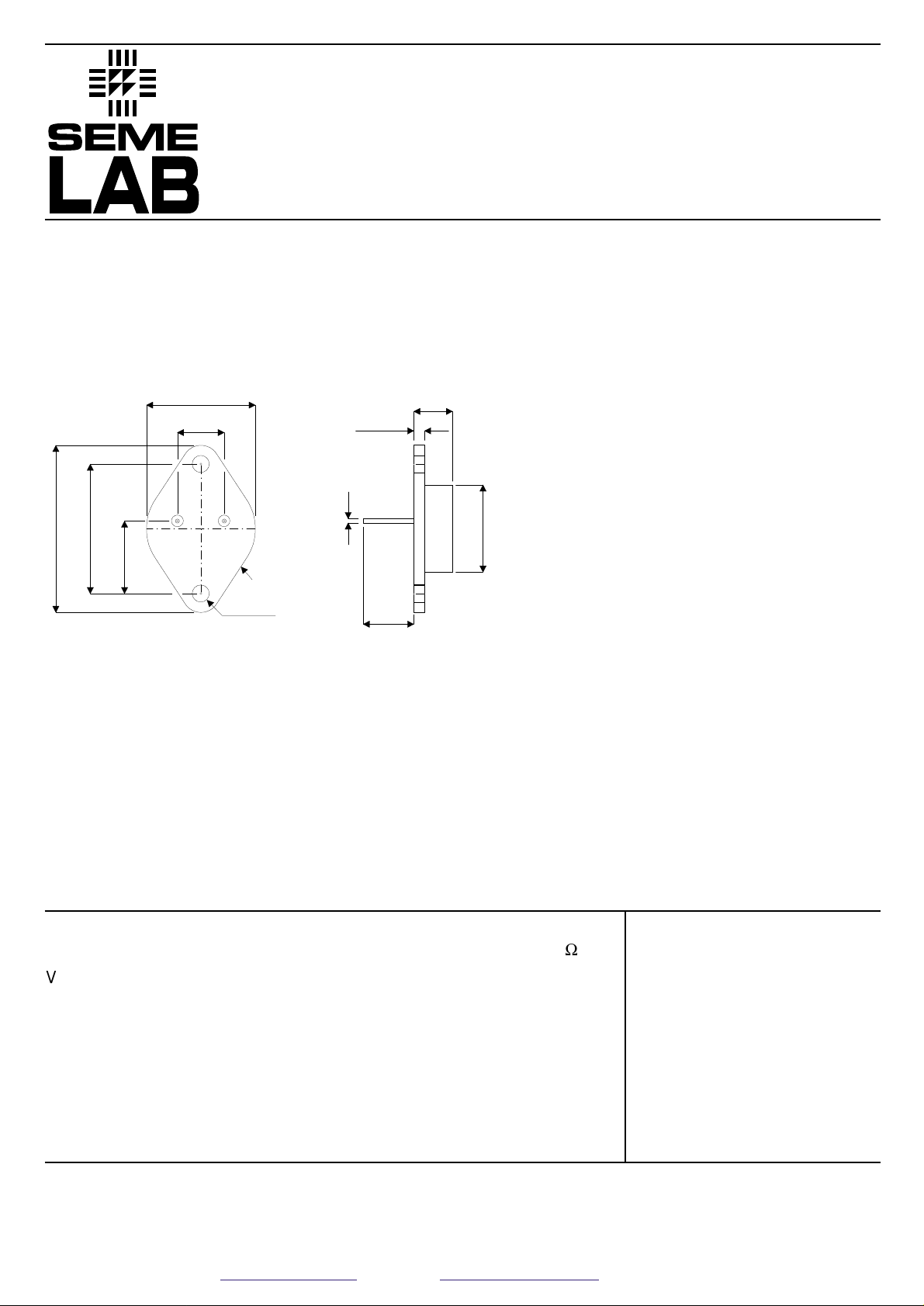
MECHANICAL DATA
Dimensions in mm (inches)
HIGH CURRENT
HIGH SPEED
HIGH POWER
SILICON NPN PLANAR
TRANSISTOR
ABSOLUTE MAXIMUM RATINGS (T
j
= 25°C unless otherwise stated)
TO–204AA (TO–3)
PIN 1 — Base PIN 2 — Emitter Case is Collector.
Applications
The BUX82 is an epitaxial silicon NPN planar
transistor that has high current and high power
handling capability and high switching speed.
This device is especially suitable for
switching–control amplifiers, power gates, switching regulators, power-switching circuits converters, inverters and control circuits.Other recommended applications include DC–RF amplifiers
and power oscillators.
38.61 (1.52)
39.12 (1.54)
29.9 (1.177)
30.4 (1.197)
16.64 (0.655)
12
17.15 (0.675)
25.15 (0.99)
26.67 (1.05)
10.67 (0.42)
11.18 (0.44)
3
(case)
3.84 (0.151)
4.09 (0.161)
0.97 (0.060)
1.10 (0.043)
1.52 (0.06)
3.43 (0.135)
7.92 (0.312)
12.70 (0.50)
6.35 (0.25)
9.15 (0.36)
max.
22.23
(0.875)

Parameter Test Conditions Min. Typ. Max. Unit
V
CEOsust
V
CERsust
V
CE(sat)
V
BE(sat)*
V
CE(sat)
V
BE(sat)*
I
EBO
I
CES
h
FE
f
T
t
on
t
s
t
f
BUX82
Prelim. 3/94
Semelab plc. Telephone +44(0)1455 556565. Fax +44(0)1455 552612.
E-mail: sales@semelab.co.uk
Website: http://www.semelab.co.uk
IC= 100mA IB= 0
L = 25mH
IC= 100mA RBE= 100
W
L = 15mH
IC= 2.5A IB= 0.5A
IC= 4A IB= 1.25A
IC= 0 VEB= 10V
V
CESMmax
VBE= 0
IC= 0.6A VCE= 5V
IC= 0.2A VCE= 10V
I
C ON
= 2.5A VCC= 250V
IB1= 0.5A IB2= 1A
Collector - Emitter Sustaining
Voltage
Collector - Emitter Sustaining
Voltage
Collector – Emitter
Saturation Voltage
Base – Emitter
Saturation Voltage
Collector – Emitter
Saturation Voltage
Base – Emitter
Saturation Voltage
Emitter Cut-off Current
Collector Cut-off Current
DC Current Gain
Transition Frequency
Turn–On Time
Storage Time
Fall Time
400
500
1.5
1.4
3
1.6
10
1
30
6
0.3 0.5
23.5
0.3
V
V
V
mA
mA
—
MHz
m
s
ELECTRICAL CHARACTERISTICS (T
j
= 25°C unless otherwise stated)
THERMAL CHARACTERISTICS
R
th j-mb
Thermal Resistance Junction to Case 1.65 °C/W
 Loading...