Seme BUX39 Datasheet

Semelab plc. Telephone +44(0)1455 556565. Fax +44(0)1455 552612.
E-mail: sales@semelab.co.uk
Website: http://www.semelab.co.uk
V
CBO
Collector – Base Voltage
V
CEX
Collector – Emitter Sustaining Voltage @ VBE= –1.5V
V
CER
Collector – Emitter Voltage @ RBE= 100
W
V
CEO(sus)
Collector – Emitter Sustaining Voltage
V
EBO
Emitter – Base Voltage
I
C
Collector Current
I
CM
Peak Collector Current
I
B
Base Current
P
tot
Total Power Dissipation
Derate above 25°C
T
stg
, T
j
Maximum Junction and Storage Temperature Range
T
L
Lead Temperature
³
1
/32inch (0.8 mm) for 10 sec. max.
120V
120V
110V
90V
7V
30A
40A
6A
120W
0.68 W / °C
–65 to 100°C
230°C
BUX39
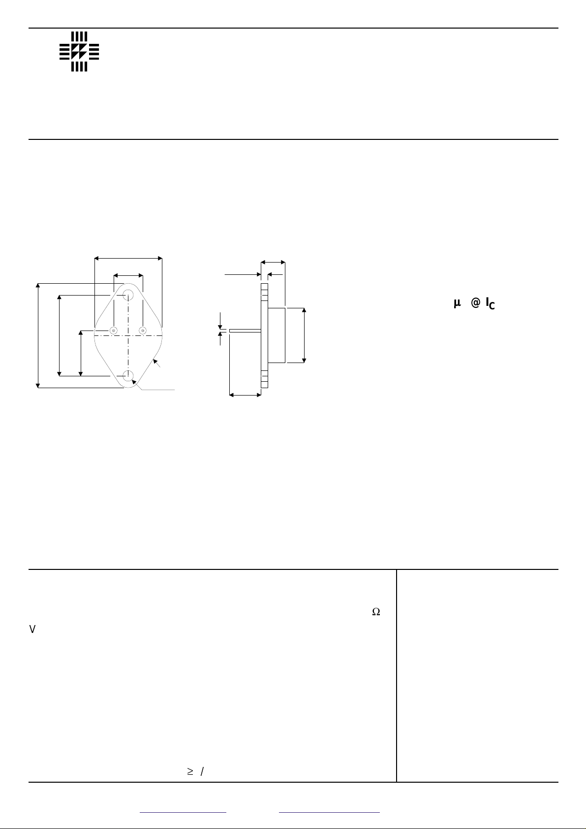
MECHANICAL DATA
Dimensions in mm (inches)
HIGH CURRENT
HIGH SPEED
HIGH POWER
SILICON NPN PLANAR
TRANSISTOR
FEATURES
• Fast Turn-On Time – 1
mmmms @ IC= 15A
• High Current Capability
ABSOLUTE MAXIMUM RATINGS (T
case
= 25°C unless otherwise stated)
Prelim. 3/94
LAB
SEME
TO–204AA (TO–3)
PIN 1 — Base
PIN 2 — Emitter
Case is Collector.
The BUX39 is in SEMELAB’s maintenance series
and is NOT recommended for new designs.
Applications
The BUX39 is an epitaxial silicon NPN planar
transistor that has high current and high power handling capability and high switching speed.
This device is especially suitable for switching–control
amplifiers, power gates, switching regulators, powerswitching circuits converters, inverters and control circuits.Other recommended applications include
DC–RF amplifiers and power oscillators.
25.15 (0.99)
26.67 (1.05)
10.67 (0.42)
11.18 (0.44)
1.52 (0.06)
3.43 (0.135)
6.35 (0.25)
9.15 (0.36)
0.97 (0.060)
38.61 (1.52)
39.12 (1.54)
29.9 (1.177)
30.4 (1.197)
16.64 (0.655)
12
17.15 (0.675)
3
(case)
3.84 (0.151)
4.09 (0.161)
1.10 (0.043)
7.92 (0.312)
12.70 (0.50)
max.
22.23
(0.875)

BUX39
Prelim. 3/94
LAB
SEME
Semelab plc. Telephone +44(0)1455 556565. Fax +44(0)1455 552612.
E-mail: sales@semelab.co.uk
Website: http://www.semelab.co.uk
Parameter Test Conditions Min. Typ. Max. Unit
IC= 0.2A IB= 0
L = 25mH
IC= 0 IE= 50mA
VCE= 70V
VCE= 120V VBE= –1.5V
VCE= 120V VBE= –1.5V
TC= 125°C
IC= 0 VBE= –5V
IC= 12A IB= 1.2A
IC= 20A IB= 2.5A
IC= 20A IB= 2.5A
IC= 12A VCE= 4V
IC= 20A VCE= 4V
VCE= 45V t = 1s
VCE= 30V t = 1s
IC= 1A VCE= 15V
IC= 20A VCC= 30V
IB= 2.5A
IC= 20A VCC= 30V
IB1= –IB2= 2.5A
Collector - Emitter Sustaining
Voltage
Emitter – Base
Breakdown Voltage
Collector Cut-off Current
Collector Cut-off Current
Emitter Cut-off Current
Collector – Emitter
Saturation Voltage
Base – Emitter
Saturation Voltage
DC Current Gain
Second Breakdown
Collector Current
Transition Frequency
Turn–On Time
Storage Time
Fall Time
90
7
1
1
5
1
0.7 1.2
1.25 1.6
2.1 2.5
15 45
8
1
4
8
0.8 1.5
0.55 1
0.15 0.3
V
V
mA
mA
mA
V
V
—
A
MHz
m
s
ELECTRICAL CHARACTERISTICS (T
case
= 25°C unless otherwise stated)
THERMAL CHARACTERISTICS
R
q
JC
Thermal Resistance Junction to Case 1.46 °C/W
V
CEO(sus)*
V
(BR)EBO
I
CEO
I
CEX
I
EBO
V
CE(sat)*
V
BE(sat)*
h
FE*
I
S/b
f
T
t
ON
t
s
t
f
 Loading...