

Seme BUL49A Datasheet
Prelim. 4/99
BUL49A
Semelab plc. Telephone +44(0)1455) 556565. Fax +44(0)1455) 552612.
E-mail: sales@semelab.co.uk
Website: http://www.semelab.co.uk
ADVANCED
DISTRIBUTED BASE DESIGN
HIGH VOLTAGE
HIGH SPEED NPN
SILICON POWER TRANSISTOR
• SEMEFAB DESIGNED AND DIFFUSED DIE
• HIGH VOLTAGE
• FAST SWITCHING
• HIGH ENERGY RATING
• EFFICIENT POWER SWITCHING
• MILITARY AND HI–REL OPTIONS
• EXCEPTIONAL HIGH TEMPERATURE
PERFORMANCE
FEATURES
• Multi–base for efficient energy distribution
across the chip resulting in significantly
improved switching and energy ratings
across full temperature range.
• Ion implant and high accuracy masking for
tight control of characteristics from batch to
batch.
• Triple Guard Rings for improved control of
high voltages.
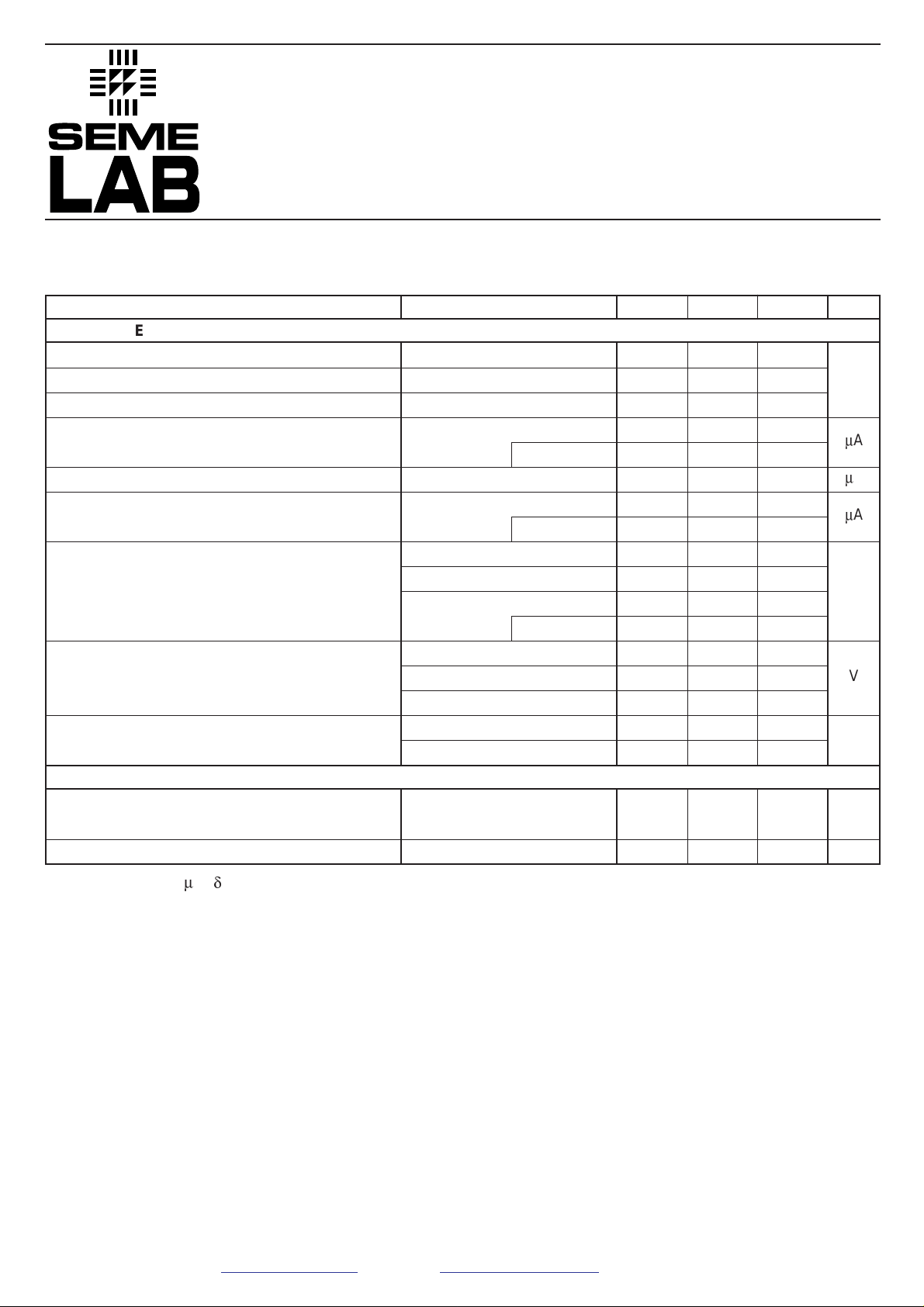
V
CBO
Collector – Base Voltage
V
CEO
Collector – Emitter Voltage (IB= 0)
V
EBO
Emitter – Base Voltage (IC= 0)
I
C
Continuous Collector Current
I
C(PK)
Peak Collector Current
P
tot
Total Dissipation at T
case
= 25°C
T
stg
Operating and Storage Temperature Range
R
th
Thermal Resistance (junction-case)
600V
300V
10V
25A
40A
200W
–65 to 175°C
Max. 0.7°CW
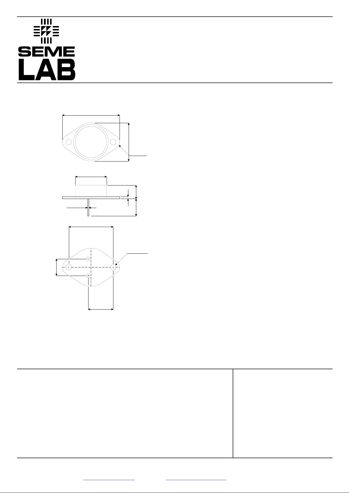
MECHANICAL DATA
Dimensions in mm
40.01 (1.575)
Max.
4.47 (0.176)
Rad.
2 Pls.
22.23 (0.875)
Max.
11.43 (0.450)
6.35 (0.250)
12.19 (0.48)
11.18 (0.44)
1.63 (0.064)
1.52 (0.060)
1.09 (0.043)
0.97 (0.038)
Dia.
30.40 (1.197)
29.90 (1.177)
16.97 (0.668)
16.87 (0.664)
4.09 (0.161)
3.84 (0.151)
2 Pls
11.18 (0.440)
10.67 (0.420)
26.67
(1.050)
Max.
2
1
Pin 1 – Base
TO3
Pin 2 – Emitter Case is Collector
ABSOLUTE MAXIMUM RATINGS (T
case
= 25°C unless otherwise stated)
BUL49A
Prelim. 4/99
Semelab plc. Telephone +44(0)1455) 556565. Fax +44(0)1455) 552612.
E-mail: sales@semelab.co.uk
Website: http://www.semelab.co.uk
Parameter Test Conditions Min. Typ. Max. Unit
V
CEO(sus)
V
(BR)CBO
V
(BR)EBO
I
CBO
I
CEO
I
EBO
h
FE*
V
CE(sat)*
V
BE(sat)*
f
t
C
ob
Collector – Emitter Sustaining Voltage
Collector – Base Breakdown Voltage
Emitter – Base Breakdown Voltage
Collector – Base Cut–Off Current
Collector – Emitter Cut–Off Current
Emitter Cut–Off Current
DC Current Gain
Collector – Emitter Saturation Voltage
Base – Emitter Saturation Voltage
Transition Frequency
Output Capacitance
300
600
10
10
100
100
10
100
30 55
20 28
15 20
0.07 0.2
0.4 0.7
1.2 1.5
1.1 1.3
1.4 2
20
260
V
m
A
m
A
m
A
—
V
V
MHz
pF
IC= 10mA
IC= 1mA
IE= 1mA
VCB= 600V
TC = 125°C
IB= 0 VCE= 300V
VEB= 5V
IC= 0 TC = 125°C
IC= 2A VCE= 4V
IC= 10A VCE= 4V
IC= 15A VCE= 4V
TC = 125°C
IC= 2A IB= 0.2A
IC= 10A IB= 1A
IC= 15A IB= 1.5A
IC= 10A IB= 1A
IC= 15A IB= 1.5A
IC= 100 VCE= 4V f =
10MHz
VCB= 20V f = 10MHz
ELECTRICAL CHARACTERISTICS (T
case
= 25°C unless otherwise stated)
* Pulse test tp= 300ms , d< 2%
ELECTRICAL CHARACTERISTICS
DYNAMIC CHARACTERISTICS
 Loading...