Seme BDS19SMD, BDS19, BDS18SMD, BDS18 Datasheet

Semelab plc. Telephone +44(0)1455 556565. Fax +44(0)1455 552612.
E-mail: sales@semelab.co.uk
Website: http://www.semelab.co.uk
4/00
BDS18 BDS18SMD
BDS19 BDS19SMD
BDS18 BDS19
V
CBO
Collector - Base voltage (IE= 0)
V
CEO
Collector - Emitter voltage (IB= 0)
V
EBO
Emitter - Base voltage (IC= 0)
I
E
, I
C
Emitter , Collector current
I
B
Base current
P
tot
Total power dissipation at T
case
£
75°C
T
stg
Storage Temperature
T
j
Junction Temperature
–120V –150V
–120V –150V
–5V
–8A
–2A
50W
–65 TO 200°C
200°C
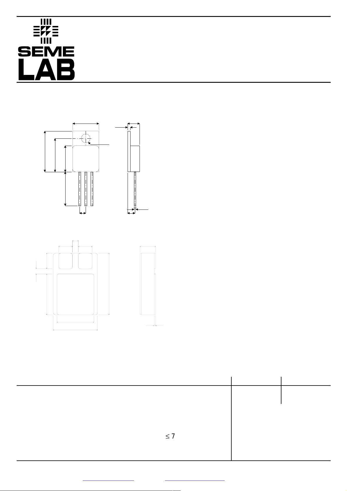
MECHANICAL DATA
Dimensions in mm
SILICON PNP
EPITAXIAL BASE IN
TO220 METAL AND
SMD1 CERAMIC SURFACE
MOUNT PACKAGES
FEATURES
• HERMETIC METAL OR CERAMIC
PACKAGES
• HIGH RELIABILITY
• MILITARY AND SPACE OPTIONS
• SCREENING TO CECC LEVELS
• FULLY ISOLATED (METAL VERSION)
APPLICATIONS
• POWER LINEAR AND SWITCHING
APPLICATIONS
• GENERAL PURPOSE POWER
ABSOLUTE MAXIMUM RATINGS (T
case
=25°C unless otherwise stated)
TO220M - TO220 Metal Package - Isolated
SMD1 - SMD1 Ceramic Surface Mount Package
Pin 1 – Base Pin 2 – Collector Pin 3 – Emitter
Semelab plc. Telephone +44(0)1455 556565. Fax +44(0)1455 552612.
E-mail: sales@semelab.co.uk
Website: http://www.semelab.co.uk
16.5
13.5
10.6
123
13.70
2.54
BSC
0.89
(0.035)
min.
3.70 (0.146)
3.41 (0.134)
4.14 (0.163)
3.84 (0.151)
min.
0.76
(0.030)
10.69 (0.421)
10.39 (0.409)
3.70 (0.146)
3.41 (0.134)
13
2
10.6
3.6
Dia.
16.02 (0.631)
0.8
15.73 (0.619)
4.6
2.70
BSC
1.0
3.60 (0.142)
Max.
9.67 (0.381)
9.38 (0.369)
11.58 (0.456)
11.28 (0.444)
0.50 (0.020)
0.26 (0.010)

Semelab plc. Telephone +44(0)1455 556565. Fax +44(0)1455 552612.
E-mail: sales@semelab.co.uk
Website: http://www.semelab.co.uk
4/00
BDS18 BDS18SMD
BDS19 BDS19SMD
Parameter Test Conditions Max. Unit
R
THj-case
Thermal resistance junction - case Max. 2.5°C/W
R
THj-a
Thermal resistance junction - ambient Max. 62.5°C/W
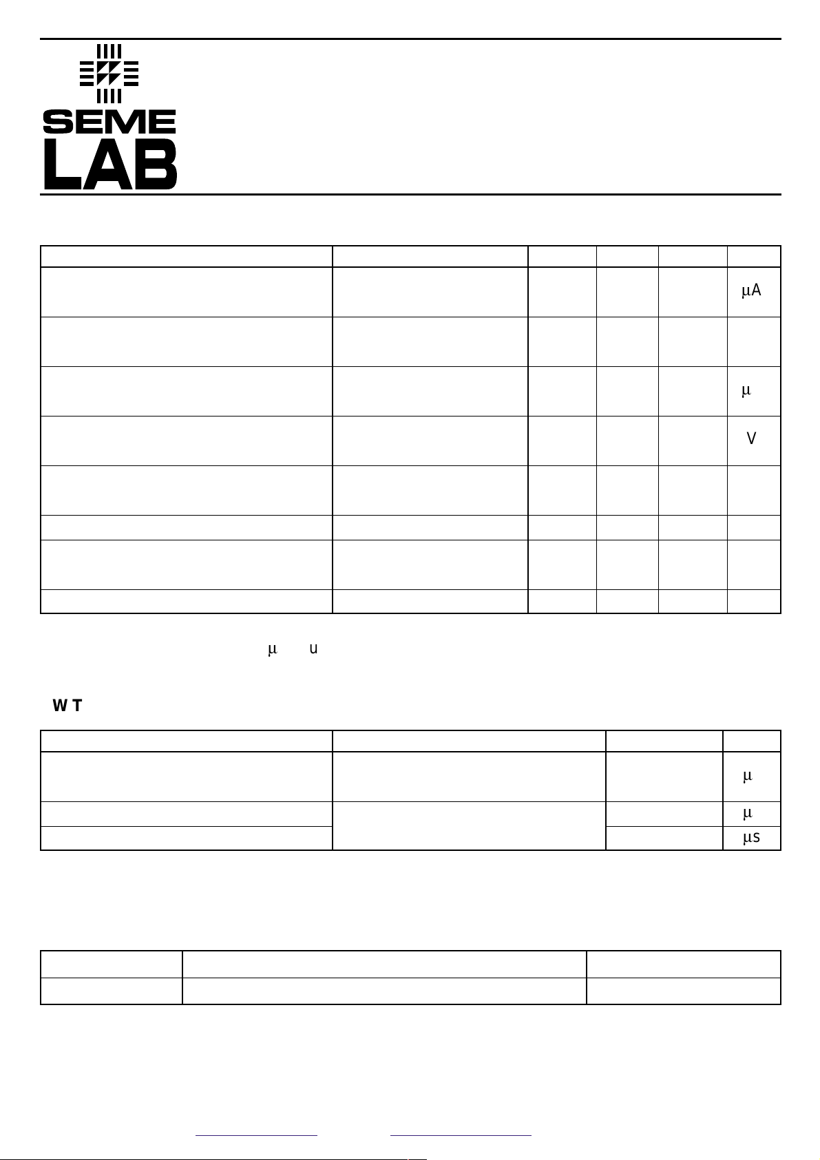
Parameter Test Conditions Min. Typ. Max. Unit
Collector cut-off current
(IE= 0)
Collector cut-off current
(IB= 0)
Emitter cut-off current
(IC= 0)
Collector - Emitter
sustaining voltage (IB= 0)
Collector - Emitter
saturation voltage
Base - Emitter voltage
DC Current gain
Transition frequency
BDS18 VCB= –120V
BDS19 VCB= –150V
BDS18 VCE= –60V
BDS19 VCE= –75V
VEB= –5V
BDS18
BDS19
IC= –1A IB= –0.1A
IC= –1A VCE= –2V
IC= –0.5A VCE= –2V
IC= –4A VCE= –2V
IC= –0.5A VCE= –10V
–20
–20
–0.1
–0.1
–10
–120
–150
–0.5
–1.0
40 250
15 150
30
m
A
mA
m
A
V
V
V
V
MHz
I
CBO
I
CEO
I
EBO
V
CEO(sus)*
V
CE(sat)*
V
BE(on)*
h
FE*
f
T
ELECTRICAL CHARACTERISTICS (T
case
= 25°C unless otherwise stated)
THERMAL DATA
IC= –100mA
t
on
t
s
t
f
On Time (td+ tr)
Storage Time
Fall Time
IC= 2A VCC= –80V
IB1= 0.2A
IC= 2A VCC= –80V
IB1= –IB2= 0.2A
0.5
1.5
0.3
m
s
m
s
m
s
SWITCHING CHARACTERISTICS
*Pulsed : Pulse duration = 300 ms , duty cycle = 1.5%
 Loading...