Seme 2N7002CSM Datasheet

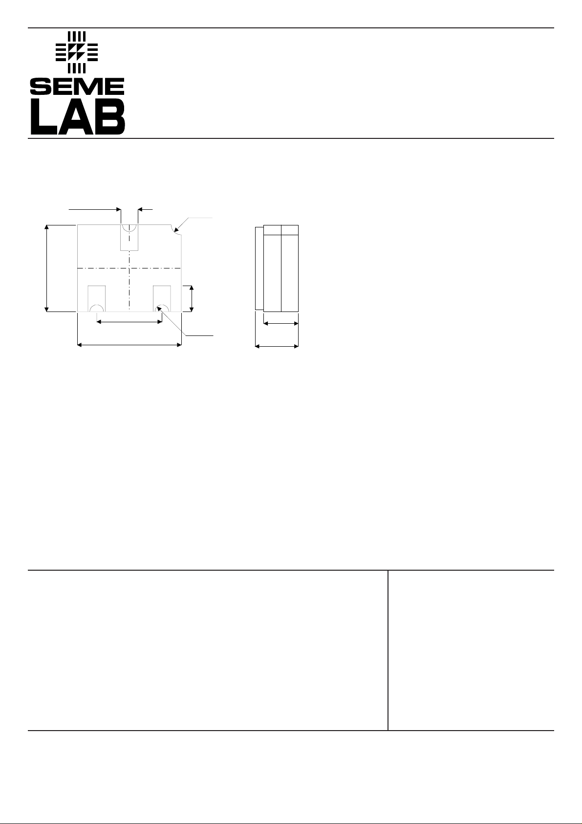
MECHANICAL DATA
Dimensions in mm (inches)
0.51 ± 0.10
(0.02 ± 0.004)
3
2.54 ± 0.13
(0.10 ± 0.005)
21
1.91 ± 0.10
(0.075 ± 0.004)
3.05 ± 0.13
(0.12 ± 0.005)
(0.012)
(0.012)
1.02 ± 0.10
A =
(0.04 ± 0.004)
0.31
0.31
2N7002CSM
N–CHANNEL
ENHANCEMENT MODE
rad.
0.76 ± 0.15
(0.03 ± 0.006)
rad.
A
1.40
(0.055)
max.
MOS TRANSISTOR
FEATURES
• V
(BR)DSS
• RDS
= 0.115A
• I
D
(ON)
= 60V
= 7.5
ΩΩ
SOT23 CERAMIC
(LCC1 PACKAGE)
Underside View
PAD 1 – Gate
PAD 2 – Source PAD 3 – Drain
ABSOLUTE MAXIMUM RATINGS (T
V
V
I
D
I
D
I
DM
P
P
T
T
DS
GS
D
D
j
stg
Drain – Source Voltage
Gate – Source Voltage
Drain Current @ T
Drain Current @ T
Pulsed Drain Current *
Power Dissipation @ T
Power Dissipation @ T
Operating Junction Temperature Range
Storage Temperature Range
CASE
= 25°C unless otherwise stated)
= 25°C
CASE
= 100°C
CASE
= 25°C
CASE
= 100°C
CASE
–55 to 150°C
–55 to 150°C
60V
±40V
±0.115A
±0.073A
0.8A
200mW
80mW
* Pulse width limited by maximum junction temperature.
Semelab plc. Telephone +44(0)1455 556565. Fax +44(0)1455 552612. e-mail sales@semelab.co.uk
Website http://www.semelab.co.uk
Prelim. 7/98

2N7002CSM
ELECTRICAL CHARACTERISTICS (T
Parameter Test Conditions Min. Typ. Max. Unit
STATIC CHARACTERISTICS
V
(BR)DSS
V
GS(th)
I
GSS
I
DSS
I
D(on)*
R
DS(on)*
V
DS(on)*
g
FS*
g
OS*
C
iss
C
oss
C
rss
t
ON
t
OFF
Gate – Source Breakdown Voltage
Gate Threshold Voltage
Gate – Body Leakage Current
Zero Gate Voltage Drain Current
On–State Drain Current
Drain – Source On Resistance
Drain – Source On Voltage
Forward Transconductance
Common Source Output Conductance
DYNAMIC CHARACTERISTICS
Input Capacitance
Output Capacitance
Reverse Transfer Capacitance
SWITCHING CHARACTERISTICS
Turn–On Time
Turn–Off Time
VGS= 0V ID= 10µA
VDS= V
VGS= ±20VVDS= 0V
VDS= 60V VGS= 0V
VDS≥2V
VGS= 5V
ID= 50mA T
VGS= 10V
ID= 0.5A T
VGS= 5V ID= 50mA
VGS= 10V
ID= 0.5A T
VDS= 10V ID= 0.2A
VDS= 5V ID= 50mA
VDS= 25V
VGS= 0V
f = 1MHz
VDD= 30V V
RL= 150Ω RG= 25Ω
ID= 0.2A
= 25°C unless otherwise stated)
CASE
GS
DS(ON)VGS
ID= 0.25mA
T
CASE
= 125°C
= 10V
= 125°C
CASE
= 125°C
CASE
= 125°C
CASE
= 10V
GEN
60 70
1 2.15 2.5
500 1000
57.5
9 13.5
2.5 7.5
4.4 13.5
0.25 0.375
1.25 3.75
2.2 6.75
80 170
500
16 50
11 25
25
720
720
±100
1
500
V
nA
µA
mA
Ω
V
ms
µs
pF
ns
* Pulse Test: PW = 80 µs , δ≤1%
Parameter Min. Typ. Max. Unit
R
θJA
Thermal Resistance, Junction to Ambient 625 °C/W
Semelab plc. Telephone +44(0)1455 556565. Fax +44(0)1455 552612. e-mail sales@semelab.co.uk
Website http://www.semelab.co.uk
Prelim. 7/98
 Loading...