Seme 2N6849 Datasheet

Semelab plc. Telephone +44(0)1455 556565. Fax +44(0)1455 552612.
E-mail: sales@semelab.co.uk
Website: http://www.semelab.co.uk
P–CHANNEL
POWER MOSFETs
V
DSS
- 100V
I
D(cont)
- 6.5A
R
DS(on)
0.30
WW
WW
Prelim. 9/00
LAB
SEME
2N6849
V
GS
Gate – Source Voltage*
V
DS
Drain – Source Voltage*
V
DG
Drain – Gate Voltage (RGS= 20kW)*
I
D
Continuous Drain Current @ TC= 25°C*
@ TC= 100°C*
I
DM
Pulsed Drain Current
2*
E
AS
Single Pulse Avalanche Current
3
P
D
Power Dissipation @ TC= 25°C*
Linear Derating Factor*
T
J
, T
STG
Operating and Storage Junction Temperature Range*
R
q
JC
Thermal Resistance Junction to Case*
R
q
JA
Thermal Resistance Junction to Ambient
±20V
-100V
-100V
–6.5A
–4.1A
–25A
500mJ
25W
0.2W/°C
–55 to +150°C
5°C/W
175°C/W
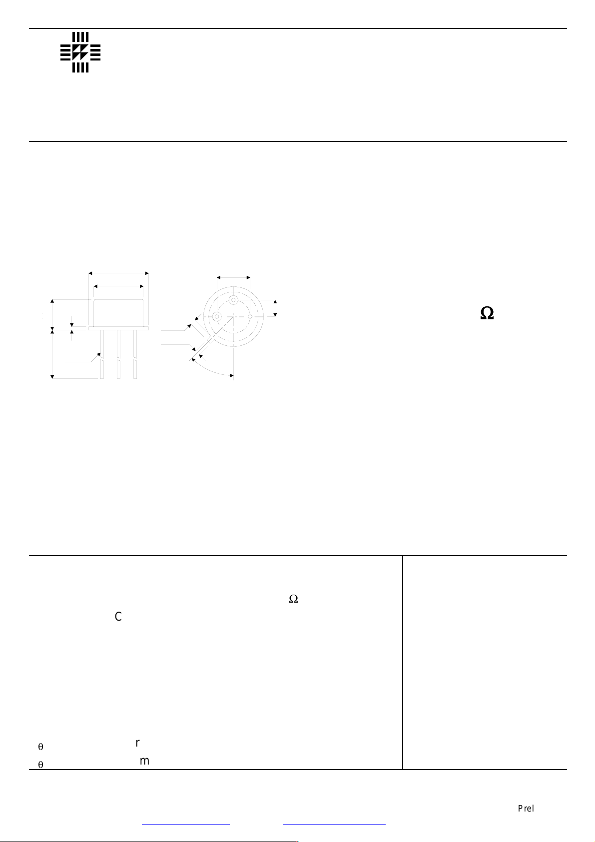
MECHANICAL DATA
Dimensions in mm (inches)
TO–39 METAL PACKAGE
ABSOLUTE MAXIMUM RATINGS (T
case
= 25°C unless otherwise stated)
4
4
Pin 1 = Emitter
Underside View
Pin 2 = Base Pin 3 = Collector
FEATURES
• Single pulse avalanche energy rated
• SOA is power dissipation limited
• Nanosecond switching speeds
• Linear transfer characteristics
• High input impedance
.19 (0.165)
.95 (0.195)
12.70
(0 .5 00 )
min.
0.89
max.
(0 .0 35 )
7.75 (0.305)
8.51 (0.335)
dia.
8.89 (0.35)
9.40 (0.37)
7.75 (0.305)
8.51 (0.335)
0.66 (0.026)
1.14 (0.045)
0.71 (0.028)
0.86 (0.034)
5.08 (0.200)
ty p .
!
45°
2.54
(0 .1 00 )

Semelab plc. Telephone +44(0)1455 556565. Fax +44(0)1455 552612.
E-mail: sales@semelab.co.uk
Website: http://www.semelab.co.uk
Prelim. 9/00
LAB
SEME
2N6849
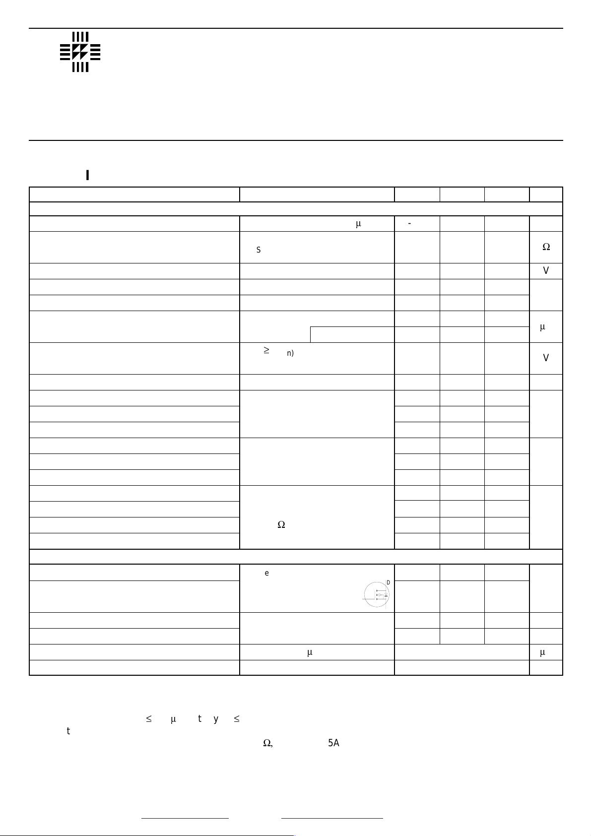
Parameter Test Conditions Min. Typ. Max. Unit
V
W
V
nA
m
A
V
(S É )
pF
nC
ns
A
V
ns
m
C
—
-100
0.30*
-2 -4
-100
100
-250
-1000
- 2.1
2.5 3.5 7.5
500
300
100
25 45
13 23
12 22
30 60
70 140
70 140
70 140
-6.5
-25
4
250
1.8
negligible
VGS= 0 ID= 250mA
VGS= -10V ID= - 4.1A
VDS= V
GS
ID= - 0.25mA
VGS= - 20V
VGS= 20V
VDS= Max rating x 0.8
VGS= 0V TC= -125°C
V
DS
³
I
D(on)RDS(on)max.
VGS= -10V ID= - 6.5A
VDS= -5V ID= - 4.1A
VGS= 0V VDS= - 25V
f = 1.0 MHz
VGS= -15V ID= - 15A
VDS= 08v Max Rating
VDD= - 42V ID= - 4.1A
Zo = 50
W
Modified MOSFETSymbol
showing the integralreverse
P-N Junction rectifier.
VGS= 0 IS= 6.5A TJ= 25°C
I
F
= - 6.5A TJ= 25°C
di
F
/dt = 100 A/ms
ELECTRICAL CHARACTERISTICS (T
case
= 25°C unless otherwise stated)
Drain – Source Breakdown Voltage*
Static Drain – Source On–State
Resistance
1
Gate Threshold Voltage*
Forward Gate
– Source Leakage
Reverse Gate
– Source Leakage
Zero Gate Voltage Drain Current*
On-State Drain Voltage
1
Forward Transconductance
1
Input Capacitance
Output Capacitance
Reverse Transfer Capacitance
Total Gate Charge
Gate – Source Charge
Gate – Drain (“Miller”) Charge
Turn–On Delay Time
Rise Time
Turn–Off Delay Time
Fall Time
Continous Source Current*
Pulse Source Current |(Body Diode)
2
Diode Forward Voltage
1
Reverse Recovery Time
Reverse Recovery Charge
Forward Turn–On Time
BV
DSS
R
DS(on)
V
GS(th)
I
GSS
I
GSS
I
DSS
V
DS(on)
g
fs
C
iss
C
oss
C
rss
Q
g
Q
gs
Q
gd
t
d(on)
t
r
t
d(off)
t
f
I
S
I
SM
V
SD
t
rr
Q
rr
t
on
STATIC ELECTRICAL RATINGS
SOURCE – DRAIN DIODE CHARACTERISTICS
*JEDEC Registered Value
1 Pulse Test: Pulse Width £300ms, duty cycle £2%
2 Repetitive Rating: Pulse width limited by max. junction temperature
3 V
DD
= 25V starting Tj= 25.°C, L=17.25mH, R
G =
25
W,
Peak IL= 6.5A
D
G
S
 Loading...