

Seme 2N6661 Datasheet
* Pulse width limited by maximum junction temperature.
Prelim. 6/94
Semelab plc. Telephone +44(0)1455 556565. Fax +44(0)1455 552612.
E-mail: sales@semelab.co.uk
Website: http://www.semelab.co.uk
2N6661
N–CHANNEL
ENHANCEMENT MODE
MOS TRANSIST OR
FEATURES
• Switching Regulators
• Converters
• Motor Drivers
V
DS
Drain – Source Voltage
V
GS
Gate – Source Voltage
I
D
Drain Current @ T
CASE
= 25°C
I
D
Drain Current @ T
CASE
= 100°C
I
DM
Pulsed Drain Current *
P
D
Power Dissipation @ T
CASE
= 25°C
P
D
Power Dissipation @ T
CASE
= 100°C
T
j
Operating Junction Temperature Range
T
stg
Storage Temperature Range
T
L
Lead Temperature (1/16” from case for 10 sec.)
90V
±20V
0.9A
0.7A
3A
6.25W
2.5W
–55 to 150°C
–55 to 150°C
300°C
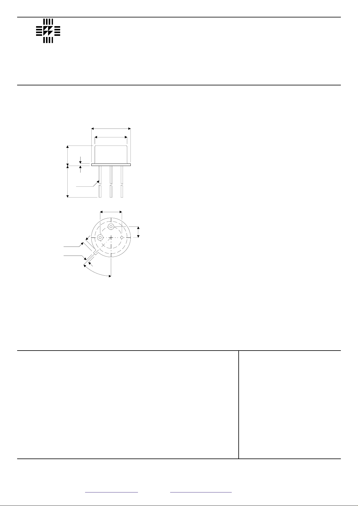
MECHANICAL DATA
Dimensions in mm (inches)
ABSOLUTE MAXIMUM RATINGS (T
CASE
= 25°C unless otherwise stated)
TO–39 METAL PACKAGE
Underside View
PIN 1 – Source
PIN 2 – Gate
PIN 3 – Drain
CASE – Drain
LAB
SEME
4.19 (0.165)
4.95 (0.195)
0.89
max.
(0.035)
12.70
(0.500)
min.
7.75 (0.305)
8.51 (0.335)
dia.
8.89 (0.35)
9.40 (0.37)
7.75 (0.305)
8.51 (0.335)
5.08 (0.200)
typ.
2.54
(0.100)
0.66 (0.026)
1.14 (0.045)
0.71 (0.028)
0.86 (0.034)
123
45˚
Prelim. 6/94
Semelab plc. Telephone +44(0)1455 556565. Fax +44(0)1455 552612.
E-mail: sales@semelab.co.uk
Website: http://www.semelab.co.uk
ELECTRICAL CHARACTERISTICS (T
CASE
= 25°C unless otherwise stated)
VGS= 0V ID= 10mA
VDS= V
GS
ID= 1mA
VGS= ±15V
VDS= 0V T
CASE
= 125°C
VDS= 90V VGS= 0V
VDS= 72V VGS= 0V
T
CASE
= 125°C
VDS= 15V VGS= 10V
VGS= 5V ID= 0.3A
VGS= 10V
ID= 1A T
CASE
= 125°C
VGS= 5V ID= 0.3A
VGS= 10V
ID= 1A T
CASE
= 125°C
VDS= 10V ID= 0.5A
VDS= 10V ID= 0.1A
VGS= 10V ID= 1A
f = 1kHz
VDS= 24V
VGS= 0V
f = 1MHz
VDD= 25V V
GEN
= 10V
RL= 23
W
RG= 25
W
ID= 1A
V
(BR)DSS
Gate – Source Breakdown Voltage
V
GS(th)
Gate Threshold Voltage
I
GSS
Gate – Body Leakage Current
I
DSS
Zero Gate Voltage Drain Current
I
D(on)*
On–State Drain Current
R
DS(on)*
Drain – Source On Resistance
V
DS(on)*
Drain – Source On Voltage
g
FS*
Forward Transconductance
g
OS*
Common Source Output Conductance
Small Signal Drain – Source
R
DS(on)
On Resistance
C
ds
Drain – Source Capacitance
C
iss
Input Capacitance
C
oss
Output Capacitance
C
rss
Reverse Transfer Capacitance
t
ON
Turn–On Time
t
OFF
Turn–Off Time
LAB
SEME
90 120
0.8 1.6 2
±100
±500
10
500
1.5 1.8
4.2 5.3
3.6 4
6.8 9
1.26 1.6
3.6 4
6.8 9
170 350
225
3.6 4
30 40
35 50
15 40
210
610
810
V
nA
m
A
A
W
V
ms
m
s
W
pF
ns
2N6661
STATIC CHARACTERISTICS
DYNAMIC CHARACTERISTICS
SWITCHING CHARACTERISTICS
* Pulse Test: tp£
80 ms , d£1%
Parameter Test Conditions Min. Typ. Max. Unit
 Loading...