Seme 2N4392CSM Datasheet

Semelab plc. Telephone (01455) 556565. Telex: 341927. Fax (01455) 552612.
Prelim. 7/94
2N4392CSM
LAB
SEME
SMALL SIGNAL
N–CHANNEL J–FET IN A
HERMETICALLY SEALED
CERAMIC SURFA CE MOUNT PACKA GE
FOR HIGH RELIABILITY APPLICATIONS
FEATURES
• HERMETIC CERAMIC SURFACE MOUNT
PACKAGE (SOT23 COMPATIBLE)
• CECC SCREENING OPTIONS
• SPACE QUALITY LEVELS OPTIONS
APPLICATIONS:
Hermetically sealed surface mount version
of the popular 2N4392 for high reliability /
space applications requiring small size
and low weight devices.
V
DS
Drain – Source Voltage
V
DG
Drain – Gate Voltage
V
GS
Gate – Source Voltage
I
G
Forward Gate Current
P
D
Power Dissipation @ TA= 25°C
Derate above 25°C
T
J
, T
STG
Operating Junction and Storage Temperature Range
40V
40V
40V
50mA
500mW
2.85mW / °C
–65 to +175°C
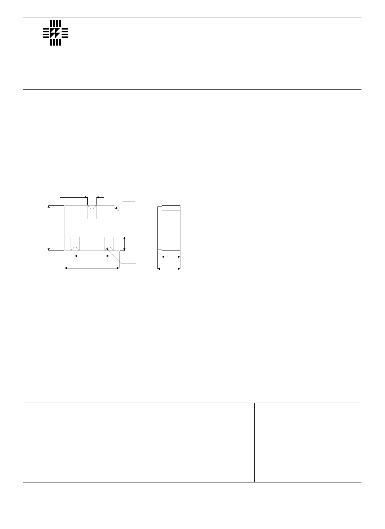
MECHANICAL DATA
Dimensions in mm (inches)
SOT23 CERAMIC
(LCC1 PACKAGE)
ABSOLUTE MAXIMUM RATINGS (T
amb
= 25°C unless otherwise stated)
PAD 1 – Source
Underside View
PAD 2 – Drain PAD 3 – Gate
21
0.51 ± 0.10
(0.02 ± 0.004)
0.31
(0.012)
1.91 ± 0.10
(0.075 ± 0.004)
3.05 ± 0.13
(0.12 ± 0.005)
2.54 ± 0.13
(0.10 ± 0.005)
0.76 ± 0.15
(0.03 ± 0.006)
1.02 ± 0.10
(0.04 ± 0.004)
1.40
(0.055)
max.
A
0.31
(0.012)
rad.
rad.
A =
3

V
nA
mA
V
Ω
pF
Ω
ns
40
–2 –5
1
0.1
0.1
25 75
0.4
60
14
3.5
60
5
20
15
35
Semelab plc. Telephone (01455) 556565. Telex: 341927. Fax (01455) 552612.
Prelim. 7/94
2N4392CSM
LAB
SEME
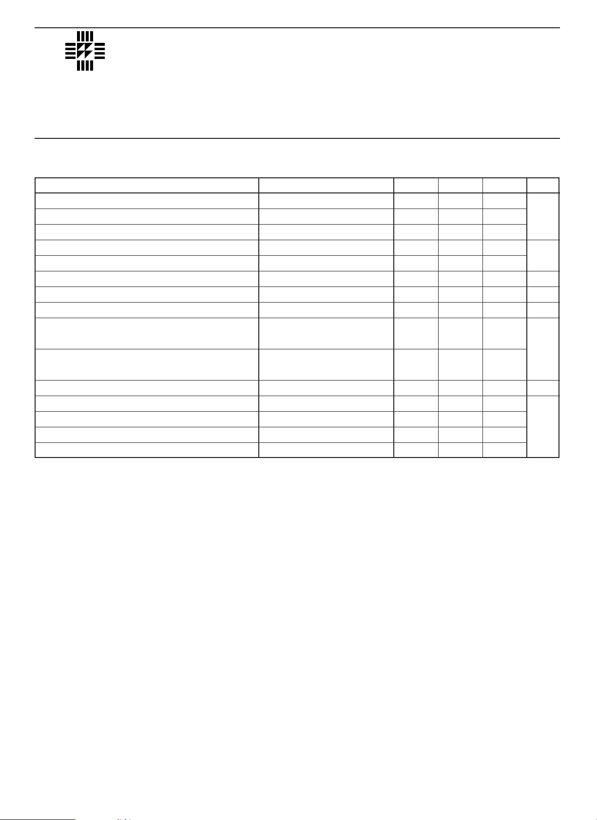
Parameter Test Conditions Min. Typ. Max. Unit
ELECTRICAL CHARACTERISTICS (T
amb
= 25°C unless otherwise stated)
VDS= 0 IG= 1µA
VDS= 20V ID= 1nA
VDS= 0 IG= 1mA
VDS= 0 VGS= 20V
VDS= 20V VGS= –7V
VDS= 20V VGS= 0
VGS= 0 ID= 6mA
VGS= 0 ID= 1mA
VDS= 20V VGS= 0
f = 1MHz
VDS= 0 VGS= –7V
f = 1MHz
VGS= 0 ID= 1mA
I
D(on)
= 6mA
V
GS(off)
= 7V
I
D(on)
= 6mA
V
GS(off)
= 7V
V
(BR)GSS
Gate – Source Breakdown Voltage
V
GS
Gate – Source Voltage
V
GS(f)
Gate – Source Forward Voltage
I
GSS
Gate Reverse Current
I
D(off)
Drain Cut–off Current
I
DSS*
Zero Gate Voltage Drain Current
V
DS(on)
Drain – Source On Voltage
R
DS(on)
Drain – Source On Resistance
C
ISS
Input Capacitance
C
RSS
Reverse Transfer Capacitance#
R
DS(on)
Static Drain – Source On Resistance
t
r
Rise Time
t
f
Fall Time
t
on
Turn-On Time
t
off
Turn-Off Time
 Loading...