Seme 2N3439CSM4R Datasheet

2N3439CSM4R
2N3440CSM4R
Prelim. 11/98
Semelab plc. Telephone +44(0)1455 556565. Fax +44(0)1455 552612. e-mail sales@semelab.co.uk
Website http://www.semelab.co.uk
HIGH V OLTA GE, MEDIUM PO WER, NPN
TRANSIST OR IN A
HERMETICALLY SEALED
CERAMIC SURFACE MOUNT PA CKA GE
FOR HIGH RELIABILITY APPLICATIONS
FEATURES
• Hermetic Ceramic 4 pin Surface Mount
Package - LCC3
• High Voltage Small Signal Type
• Full Screening Options Available
• “R” Denotes Reverse Pinning
APPLICATIONS:
The 2N3439CSM4 and 2N3440CSM4 are high
voltage silicon epitaxial planar transistors mounted
in the popular 4 pin ceramic surface mount
hermetically sealed package. These products are
specifically intended for use in High reliability
systems and can be ordered with a full range of
screening options from standard Military
(equivalent to CECC Full Assessment Level)
through all options up to full space flight level.
V
CBO
Collector – Base Voltage (IE= 0)
V
CEO
Collector – Emitter Voltage (IB= 0)
V
EBO
Emitter – Base Voltage (IB= 0)
I
C
Collector Current.
I
B
Base Current.
P
tot
Total Power Dissipation at T
amb
= 25°C with product
mounted on a suitable PCB to provide a heat path.
T
stg
Storage Temperature.
T
j
Maximum Junction Temperature.
450V
350V
7V
1A
0.5A
0.5W
300V
250V
7V
1A
0.5A
0.5W
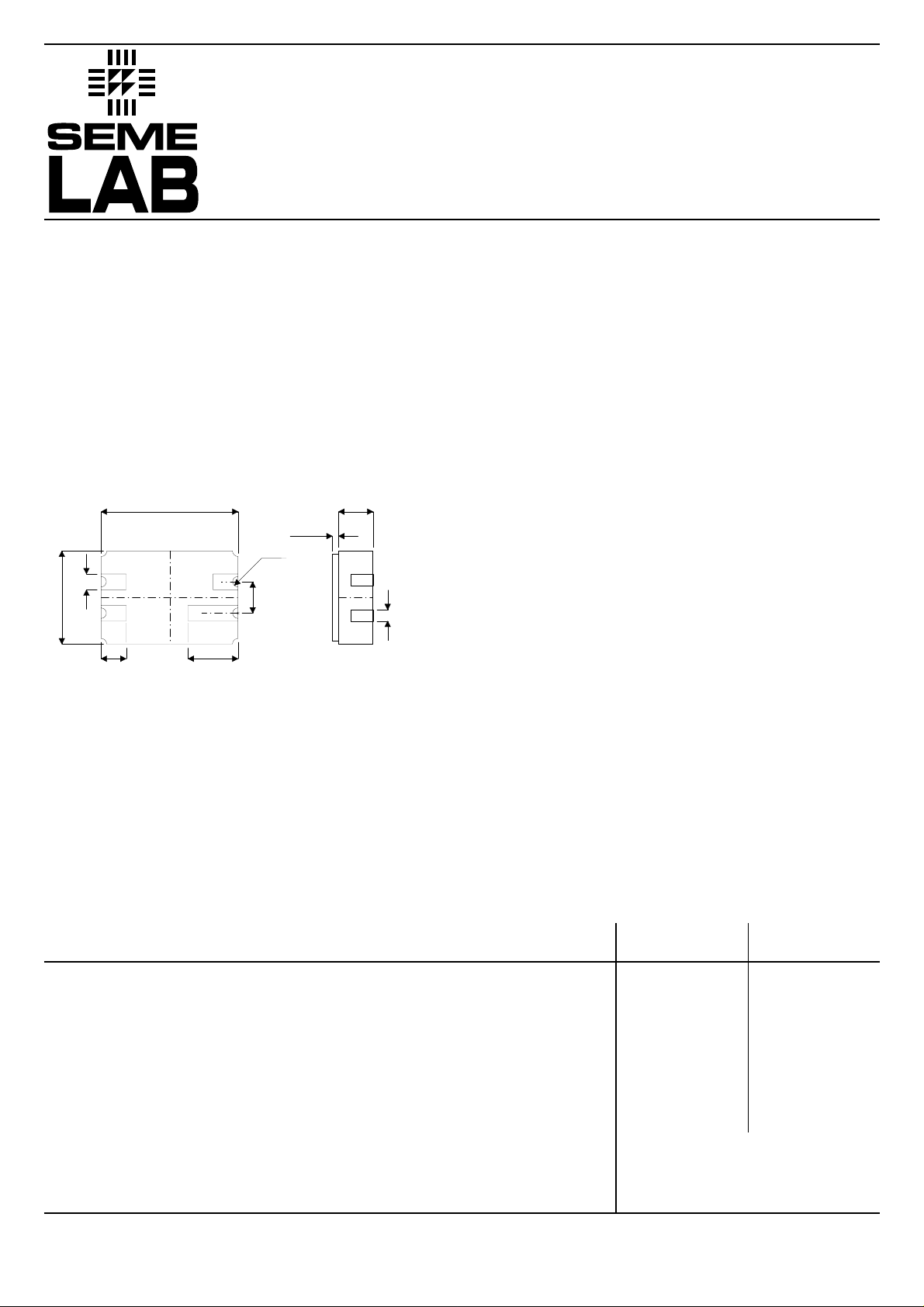
MECHANICAL DATA
Dimensions in mm (inches)
ABSOLUTE MAXIMUM RATINGS
LCC3 PACKAGE
Underside View
PAD 1 – Collector
PAD 2 – Emitter
PAD 3 – N/C
PAD 4 – Base
2N3439CSM4 2N3440CSM4
–65 to +200°C
+200°C
0.64 ± 0.08
(0.025 ± 0.003)
3.81 ± 0.13
(0.15 ± 0.005)
4
1.02 ± 0.20
(0.04 ± 0.008)
5.59 ± 0.13
(0.22 ± 0.005)
23
1
2.03 ± 0.20
(0.08 ± 0.008)
1.40 ± 0.15
(0.055 ± 0.006)
0.25 ± 0.03
(0.01 ± 0.001)
0.23
rad.
(0.009)
1.27 ± 0.05
(0.05 ± 0.002)
0.23
(0.009)
min.

Parameter Test Conditions Min. Typ. Max. Unit
350
250
500
500
20
20
20
50
20
0.5
1.3
40
30
2N3439CSM4R
2N3440CSM4R
Prelim. 11/98
Semelab plc. Telephone +44(0)1455 556565. Fax +44(0)1455 552612. e-mail sales@semelab.co.uk
Website http://www.semelab.co.uk
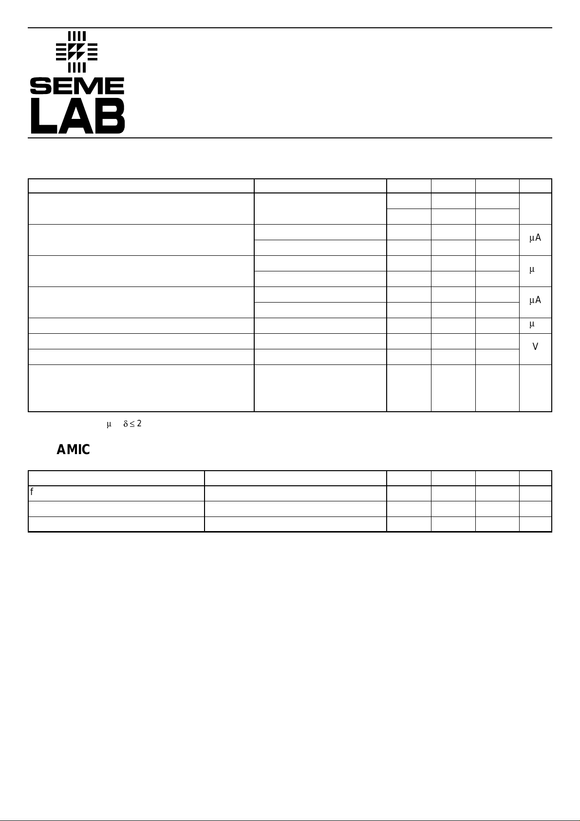
Parameter Test Conditions Min. Typ. Max. Unit
2N3439CSM4R
2N3440CSM4R
2N3439CSM4R
2N3440CSM4R
VCB= 360V 2N3439CSM4R
VCB= 250V 2N3440CSM4R
VCE= 300V 2N3439CSM4R
VCE= 200V 2N3440CSM4R
VEB= 6V
IC= 50mA IB= 4mA
IC= 50mA IB= 4mA
IC= 20mA VCE= 10V
2N3439CSM4R only
IC= 20mA VCE= 10V
ELECTRICAL CHARACTERISTICS (T
case
= 25°C unless otherwise stated)
V
CEO(sus)*
Collector – Emitter Sustaining Voltage
(IB= 0)
I
CEX*
Collector Cut-off Current
(VBE= –1.5V)
I
CBO*
Collector – Base Cut-off Current
(IE= 0)
I
CEO*
Collector – Cut-off Current
(IB= 0)
I
EBO*
Emitter Cut-off Current (IC= 0)
V
CE(sat)*
Collector – Emitter Saturation Voltage
V
BE(sat)*
Base – Emitter Saturation Voltage
h
FE*
DC Current Gain
V
m
A
m
A
m
A
m
A
V
—
f
T
Transition Frequency
C
ob
Output Capacitance
h
fe
Small Signal Current Gain
IC= 10mA VCE= 10V f = 5MHz
VCB= 10V f = 10MHz
IC= 5mA VCE= 10V f = 1kHz
15
10
25
MHz
pF
* Pulse test tp = 300ms ,
d £
2%
DYNAMIC CHARACTERISTICS (T
case
= 25°C unless otherwise stated)
IC= 50mA
 Loading...