


THIS DOCUMENT CONTAINS PROPRIETARY INFORMATION AND SUCH
INFORMATION MAY NOT BE DISCLOSED TO OTHERS FOR ANY
PURPOSES WITHOUT WRITTEN PERMISSION FROM
SELEX Sistemi Integrati Inc.
Copyright © 2008, SELEX Sistemi Integrati Inc.
Operations and Maintenance Manual
Model 1150A Doppler
VHF Omnirange (DVOR)
571150A-0002 Rev - November, 2008
SELEX Sistemi Integrati Inc.
11300 West 89th Street
Overland Park, KS U.S.A. 66214

THIS SHEET INTENTIONALLY BLANK

SAFETY SUMMARY
The following are general safety precautions that are unrelated to specific procedures and therefore do not appear
elsewhere in this publication. These are recommended precautions that personnel should understand and apply
during through the many phases of operation and maintenance.
ELECTROSTATIC SENSITIVE DEVICES PRECAUTIONS
Since most modules used in all models of equipment have Electrostatic Discharge (ESD) sensitive devices included
in them, all modules should be considered sensitive to electrostatic discharge. Handling in the field shall be the
same as in the factory. Each system is shipped with a wrist strap that must be worn while maintaining the
equipment. The wrist strap shall be fastened to the equipment chassis either in the designated plug-in or attached to
the equipment chassis with the alligator clip. The wrist strap must be used before any modules are removed from
the equipment and at all times while handling the modules until they are placed in a protective environment such as
an anti-static bag. Modules or boards must not be placed on any non-conducting surface such as wooden work
benches, painted metal work benches, plastics, or technical manuals. Any work surface to be used must have a
conducting mat placed on it and attached to earth ground. The mat and additional wrist straps can be obtained from
SELEX Sistemi Integrati Inc.
KEEP AWAY FROM LIVE CIRCUITS
Operating personnel must at all times observe all safety regulations. Under no circumstances should any person
remove any protective covers that expose lethal voltages. Do not replace components or make adjustments inside
the equipment with primary power supply turned on. Under certain conditions, dangerous potentials may exist when
the power is in the off position, due to charges retained by capacitors. To avoid casualties, always remove power
and allow time for the capacitors to discharge before touching it.
DO NOT SERVICE OR ADJUST ALONE
Under no circumstances should any person reach into or enter the enclosure for the purpose of servicing or adjusting
the equipment except in the presence of someone who is capable of rendering aid.
RESUSCITATION
Personnel working with or near high voltages should be familiar with modern methods of resuscitation.

THIS SHEET INTENTIONALLY BLANK

SELEX Sistemi Integrati Inc.
This equipment is supplied by SELEX Sistemi Integrati Inc. For replacement parts and repair service, contact
SELEX Sistemi Integrati Inc. using the contact information provided below.
HOW TO ORDER REPLACEMENT PARTS
When ordering replacement parts, you should contact SELEX Sistemi Integrati Inc. by fax, phone or email. Please
address the following items (as applicable) in your correspondence to enable us to provide the best possible service.
1. SELEX Sistemi Integrati Inc. model number, type and serial number of equipment.
2. Unit sub-assembly number (where applicable).
3. Item or reference symbol number from parts list or schematic.
4. SELEX Sistemi Integrati Inc. part number and description.
5. Manufacturer's code, name and part number (where applicable).
6. Quantity of each replacement part required.
HOW TO REQUEST REPAIR SERVICE
In order to ensure prompt attention, parts returned for repair should have the following:
1. RMA number (Return Material Authorization number), assigned prior to return when requesting
repair service.
2. Unit part number
3. Site location
4. System information
5. Ship-to address for return
6. Contact name and number
7. Date and time of request
CONTACT INFORMATION
SELEX Sistemi Integrati Inc.
11300 W 89th Street
Overland Park KS, 66214, USA
Main Switchboard: (913) 495-2600
Main Fax: (913) 492-0870
Toll free: (800) 331-2744
CSM Direct Phone: (913) 495-2625
CSM E-mail: Support@selex-si-us.com
World Wide Web URL: www.selex-si-us.com

THIS SHEET INTENTIONALLY BLANK

MANUFACTURER’S WARRANTY
SELEX Sistemi Integrati Inc.
The following warranty is applicable in all cases, except where modified or superseded by specific contract terms.
Contact SELEX Sistemi Integrati Inc. if clarification is required.
A. The Manufacturer warrants to the original Purchaser, subject to the limitations and exclusions stated below,
that mechanical and electrical parts of products which it manufactures, (the “Products” will be free of
defects in materials and workmanship for a period of (I) one (1) year from the date of installation or (ii) 18
months from the date of shipment, whichever first occurs (the “Warranty Period”).
B. If the Customer believes a Product is defective, notice thereof shall be provided to the Manufacturer’s
Customer Service Department at the address provided on the cover page and (if applicable) to the selling
distributor. A defect in material and workmanship covered by this warranty shall be deemed to have
occurred only if, and as of the time when, the Manufacturer is notified in writing by the Customer, within
the Warranty Period, that the Product has become defective, and the Manufacturer’s personnel verify that
the said Product, in fact, does not comply with the warranty provided hereunder and it is determined that:
(i) The Products, during the entire Warranty Period, have been operated within normal service
conditions, recommended by the Manufacturer and recognized in the industry, and
(ii) The Products have been installed and adjusted according to the Manufacturer’s procedures as
stated in the Instruction Manual or other instructions supplied in writing by the Manufacturer.
C. Failures caused by lightning or other acts of God, or power surges, are not considered to be defects in
materials and workmanship and are not covered under this warranty. Routine Maintenance and calibration
are also not considered to be defects in materials and workmanship and are not covered under this
warranty. Any change, modification or alteration of the Manufacturer’s Products not specifically
authorized by the Manufacturer will void this warranty.
D. If it is determined that the conditions for warranty coverage, as described above, have been satisfied, the
Manufacturer shall repair or replace the defective products or parts thereof in accordance with the
following procedures:
(i) Customer will contact the Manufacturer’s customer Service Department which will issue the
Customer a Return Authorization (RA) number.
(ii) The Component, defective part, or Product, as appropriate, shall be returned to the Manufacturer
for inspection, freight prepaid by the customer. The Component, defective part, or Product MUST
be packaged with an industry standard anti-static protective bag sufficient to prevent any ESD
intrusion during handling and shipment, and MUST ALSO be packaged to protect from damage
due to rough handling encountered during shipment. FAILURE TO COMPLY WITH THIS
REQUIREMENT WILL VOID THE WARRANTY OF THE RETURNED ITEM. The RA
number must be clearly displayed on the exterior of the shipping container. No shipments will be
accepted without a RA number. All custom duties, fees, etc. will be paid by the Customer.
(iii) If, upon inspection it is determined by Manufacturer’s personnel that the Product or component
thereof is indeed defective and covered by this warranty, then Manufacturer, at its option, may
either repair the Product or defective components thereof and return the same to the Customer or
ship a replacement for the defective Product or part thereof, freight paid. All customs duties, fees,
etc. will be paid by the Customer. The Product or component thereof will be returned to the
Customer utilizing a shipping mode similar to that used by Customer to ship the same to the
Manufacturer.
(iv) If, upon inspection by Manufacturer, it is determined that the Product or component thereof was
not defective or was not covered by this warranty, then the cost of all of Manufacturer’s
inspections and the return shipping charges will be charged to Customer.
E. The Manufacturer reserves the right to make modifications and alterations to Products without obligation to
install such improvements on, in, or in place of theretofore manufactured products of Manufacturer.

MANUFACTURER’S WARRANTY (cont.)
F. Manufacturer does not warranty any Products, components, subassemblies, or parts not of its own
manufacture. Manufacturer hereby transfers to Customer any and all warranties (if any) which it receives
from its suppliers.
G. Periodic calibration / re-calibration of test equipment is not covered under this or any Seller’s warranty, and
is the sole responsibility of the Purchaser.
H. Any and all claims for shortages, missing or damaged items must be presented, in writing, to the Seller
within 120 days of the date of shipment from Seller’s factory.
I. This warranty applies only to the original purchaser and, unless Customer receives the express written
consent of an officer of Manufacturer, this warranty may not be assigned, transferred, or conveyed to any
third party, even if the third party is a bon a fide purchaser of the Products.
J. THIS WARRANTY IS EXPRESSLY IN LIEU OF ALL OTHER WARRANTIES, EXPRESSED OR
IMPLIED, WHETHER STATUTORY OR OTHERWISE, INCLUDING IMPLIED WARRANTY
OF MERCHANTABILITY OR FITNESS FOR A PARTICULAR PURPOSE. IN NO EVENT
SHALL THE MANUFACTURER BE LIABLE FOR INDIRECT, INCIDENTAL, COLLATERAL,
PUNITIVE, OR CONSEQUENTIAL DAMAGES OF ANY KIND, WHETHER ARISING OUT OF
CONTRACT, TORT, NEGLIGENCE, STRICT LIABILITY OR OTHER PRODUCTS LIABILITY
THEORY.
K. CUSTOMER’S SOLE REMEDY FOR ANY BREACH OF THE WARRANTY SHALL BE THE
REPAIR OR REPLACEMENT OF THE PRODUCTS BY THE MANUFACTURER AS
PROVIDED HEREIN, AND IN NO EVENT SHALL THE MANUFACTURER BE REQUIRED TO
INCUR COSTS FOR THE REPAIR OR REPLACEMENT OF ANY PRODUCT IN EXCESS OF
THE PURCHASE PRICE OF SUCH PRODUCT, PLUS ANY TRANSPORTATION CHARGES
ACTUALLY PAID ATTRIBUTABLE TO SUCH PRODUCTS.

Model 1150A DVOR
TABLE OF CONTENTS
ragraph
Pa
# Description Page #
1 GENERAL INFORMATION AND REQUIREMENTS......................................................................1-1
1.1 INTRODUCTION ................................................................................................................................1-1
1.2 EQUIPMENT DESCRIPTION.............................................................................................................1-2
1.2.1 Electronics Cabinet...............................................................................................................................1-2
1.2.1.1 Local Control Unit (LCU) (1A1)..........................................................................................................1-3
1.2.1.2 Synthesizer Assembly (1A3A1, 1A3A11)............................................................................................1-3
1.2.1.3 Audio Generator CCA (1A3A2, 1A3A9) .............................................................................................1-3
1.2.1.4 Monitor CCA (1A3A3, 1A3A10).........................................................................................................1-7
1.2.1.5 Low Voltage Power Supply (LVPS) CCA (1A3A4, 1A3A8)...............................................................1-7
1.2.1.6 Test Generator CCA (1A3A5)..............................................................................................................1-7
1.2.1.7 Remote Monitoring System (RMS) Processor CCA ( 1A3A6)............................................................1-7
1.2.1.8 Facilities CCA (1A3A7) .......................................................................................................................1-7
1.2.1.9 Sideband Amplifier Assembly (1A4A1, 1A4A2, 1A4A6, 1A4A7)......................................................1-7
1.2.1.10 RF Monitor Assembly (1A4A4)...........................................................................................................1-7
1.2.1.11 Commutator Control CCA (1A4A5).....................................................................................................1-7
1.2.1.12 Battery Charging Power Supply (BCPS) Assembly (1A5A1, 1A5A2) ................................................1-8
1.2.1.13 Carrier Power Amplifier Assembly (1A5A3, 1A5A4)..........................................................................1-8
1.2.1.14 Interface CCA (1A9).............................................................................................................................1-8
1.2.1.15 AC Power Monitor Assembly (1A6) ....................................................................................................1-8
1.2.1.16 Commutator CCA (1A10, 1A11)..........................................................................................................1-8
1.2.2 Portable Maintenance Data Terminal (PMDT) .....................................................................................1-8
1.2.3 Transmitting Antenna System...............................................................................................................1-9
1.2.3.1 Carrier Antenna.....................................................................................................................................1 -9
1.2.3.2 Sideband Antenna...............................................................................................................................1-12
1.2.3.3 Balun...................................................................................................................................................1-13
1.2.3.4 Tuning Stub.........................................................................................................................................1-14
1.2.3.5 Positioning Piece.................................................................................................................................1-14
1.2.3.6 Pedestal...............................................................................................................................................1-14
1.2.3.7 Radome ...............................................................................................................................................1-14
1.2.4 Field Monitor Antenna........................................................................................................................1-15
1.2.5 Counterpoise .......................................................................................................................................1-15
1.2.6 Equipment Shelter............................................................................................................................... 1 -16
1.2.7 Battery Backup Unit (Optional)..........................................................................................................1-16
1.3 EQUIPMENT SPECIFICATION DATA...........................................................................................1-16
1.3.1 Transmitter and Antenna System........................................................................................................1-16
1.3.1.1 Transmitter ..........................................................................................................................................1-16
1.3.1.2 Antenna System..................................................................................................................................1-18
1.3.1.3 Field Monitor......................................................................................................................................1-18
1.3.2 Monitor ...............................................................................................................................................1-19
1.3.3 Mechanical and Electrical...................................................................................................................1-20
1.3.4 Remote Control System......................................................................................................................1-20
1.3.4.1 Design Features...................................................................................................................................1 -20
1.3.4.2 RCSU Controls and Indicators............................................................................................................1 -21
1.3.4.3 RSU Controls and Indicators ..............................................................................................................1-21
1.3.5 Remote Maintenance Monitoring System (RMM) .............................................................................1-22
1.3.5.1 Design Features...................................................................................................................................1 -22
1.3.5.2 RMM Functions..................................................................................................................................1-22
1.4 EQUIPMENT AND ACCESSORIES SUPPLIED.............................................................................1-23
1.5 OPTIONAL EQUIPMENT.................................................................................................................1-23
2 TECHNICAL DESCRIPTION.............................................................................................................2-1
2.1 INTRODUCTION ................................................................................................................................2-1
Rev. - November, 2008
This document contains proprietary information and such information may not be disclosed
to others for any purposes without written permission from SELEX Sistemi Integrati Inc.
i

Model 1150A DVOR
TABLE OF CONTENTS (cont.)
Paragraph
# Description Page #
2.2 OPERATING PRINCIPLES.................................................................................................................2-1
2.2.1 DVOR Antenna Principles....................................................................................................................2-3
2.3 DVOR TRANSMITTER THEORY OF OPERATION........................................................................2-3
2.3.1 Simplified System Block Diagram........................................................................................................2-3
2.3.1.1 Electronics Cabinet (Unit 1)..................................................................................................................2-6
2.3.2 System Block Diagram Theory.............................................................................................................2-6
2.3.2.1 Frequency Synthesizer (1A3A1, 1A3A11)...........................................................................................2-7
2.3.2.1.1 Frequency Synthesizer Block Diagram Theory....................................................................................2-7
2.3.2.1.2 Frequency Synthesizer (1A3A1, 1A3A11) Detailed Circuit Theory....................................................2-9
2.3.2.1.2.1 Frequency Reference Circuitry.............................................................................................................2-9
2.3.2.1.2.2 Carrier PLL Synthesizer Circuitry......................................................................................................2-10
2.3.2.1.2.3 Carrier Phase Control Loop ................................................................................................................2-12
2.3.2.1.2.4 Sideband RF Generation Loops..........................................................................................................2-14
2.3.2.2 Audio Generator CCA (1A7, 1A23) Theory.......................................................................................2-15
2.3.2.2.1 Audio Generator CCA Block Diagram Theory...................................................................................2-15
2.3.2.3 Audio Generator CCA Detailed Circuit Theory..................................................................................2-17
2.3.2.4 CSB Power Amplifier Assembly (1A5A3, 1A5A4)...........................................................................2-19
2.3.2.4.1 CSB Power Amplifier Assembly Block Diagram Theory ..................................................................2-19
2.3.2.4.2 Power Amplifier Assembly Detailed Circuit Theory..........................................................................2 -20
2.3.2.5 Bi-Directional Coupler (1DC1)...........................................................................................................2-22
2.3.2.6 Sideband Generator Assembly (1A4A1, 1A4A2, 1A4A6, 1A5A7)....................................................2-22
2.3.2.6.1 Sideband Generator Assembly Block Diagram Theory......................................................................2-22
2.3.2.6.2 Sideband Generator CCA Detailed Circuit Theory.............................................................................2-24
2.3.2.7 RF Monitor Assembly (1A4A4) Theory.............................................................................................2-27
2.3.2.8 RF Monitor Assembly Block Diagram Theory...................................................................................2-27
2.3.2.8.1 RF Monitor Assembly (1A2) Detailed Circuit Theory.......................................................................2-28
2.3.2.9 RMS Processor Block Diagram Theory..............................................................................................2-30
2.3.2.9.1 RMS CCA Detailed Theory................................................................................................................2-32
2.3.2.10 Facilities CCA Theory........................................................................................................................2-34
2.3.2.10.1 Facilities CCA Detailed Theory..........................................................................................................2-36
2.3.2.11 Interface CCA Theory.........................................................................................................................2-38
2.3.2.12 Interface CCA Block Diagram Theory...............................................................................................2-38
2.3.2.12.1 Interface CCA Detailed Theory..........................................................................................................2-39
2.3.2.13 AC Power Monitor CCA Theory........................................................................................................2-40
2.3.2.13.1 AC Power Monitor CCA Block Diagram Theory...............................................................................2-41
2.3.2.13.2 AC Power Monitor CCA Detailed Theory..........................................................................................2-41
2.3.2.14 Local Control Unit Theory..................................................................................................................2-42
2.3.2.14.1 Local Control Unit Block Diagram Theory ........................................................................................2-43
2.3.2.14.1.1 DC to DC Converter ...........................................................................................................................2-43
2.3.2.14.1.2 Power Fail Detectors...........................................................................................................................2-43
2.3.2.14.1.3 Key Switch Registers..........................................................................................................................2-43
2.3.2.14.1.4 Parallel Interface .................................................................................................................................2-43
2.3.2.14.1.5 1.8432MHz Oscillator/Divider Chains ...............................................................................................2-44
2.3.2.14.1.6 Positive Alarm Register......................................................................................................................2-44
2.3.2.14.1.7 Negative Alarm Register.....................................................................................................................2-44
2.3.2.14.1.8 20 Second Delay Counter ...................................................................................................................2-44
2.3.2.14.1.9 LCU Transfer Control State Machine #1 and #2 and Discrete Controls.............................................2-45
2.3.2.14.1.10 LED Control........................................................................................................................................2-45
2.3.2.14.1.11 Audible Alarm ....................................................................................................................................2-45
2.3.2.14.1.12 Monitor Alarm Interface.....................................................................................................................2-45
2.3.2.14.1.13 Station Control Logic..........................................................................................................................2-45
ii Rev. - November, 2008
This document contains proprietary information and such information may not be disclosed
to others for any purposes without written permission from SELEX Sistemi Integrati Inc.

Model 1150A DVOR
TABLE OF CONTENTS (cont.)
ragraph
Pa
# Description Page #
2.3.2.14.1.14 System Configuration Inputs...............................................................................................................2-46
2.3.2.15 Test Generator (1A3A5) CCA Theory................................................................................................2-46
2.3.2.15.1 Test Generator CCA Block Diagram Theory...................................................................................... 2 -46
2.3.2.15.2 Test Generator CCA Detailed Circuit Theory.....................................................................................2-48
2.3.2.16 Low Voltage Power Supply (1A3A4, 1A3A8) CCA Theory.............................................................2-50
2.3.2.16.1 Low Voltage Power Supply (LVPS) CCA Block Diagram Theory....................................................2-50
2.3.2.16.2 Low Voltage Power Supply (LVPS) CCA Detailed Circuit Theory...................................................2-51
2.3.2.17 Monitor CCA (1A3A3, 1A3A9) Theory............................................................................................. 2 -52
2.3.2.17.1 Monitor CCA Block Diagram Theory ................................................................................................2-52
2.3.2.17.2 Monitor CCA Detailed Circuit Theory...............................................................................................2-55
2.3.2.18 Power Panel Theory............................................................................................................................2-61
2.3.2.19 Battery Charger Power Supply (BCPS) Theory..................................................................................2-61
2.3.2.19.1 BCPS CCA Block Diagram Theory....................................................................................................2-61
2.3.2.20 Battery Charger Detailed Circuit Theory............................................................................................2-63
2.3.2.21 Extender Board Block Diagram Theory..............................................................................................2-65
2.3.2.22 Commutator Control CCA Theory......................................................................................................2-66
2.3.2.22.1 Commutator Control CCA Block Diagram Theory............................................................................2-67
2.3.2.22.2 Commutator Control CCA Detailed Circuit Theory...........................................................................2-68
2.3.2.23 Commutator CCA (1A10, 1A11) Theory ...........................................................................................2-72
2.3.2.23.1 Commutator CCA Block Diagram Theory .........................................................................................2-72
2.3.2.23.2 Commutator CCA (2A2, 2A3) Detailed Circuit Theory.....................................................................2-74
2.4 PMDT (Portable Maintenance Data terminal (UNIT 2)......................................................................2-76
2.5 BATTERIES (UNIT 3).......................................................................................................................2-76
2.6 FIELD MONITOR KIT (UNIT 4)......................................................................................................2-76
3 OPERATION....................................................... ............................................................................ .....3-1
3.1 Introduction...........................................................................................................................................3-1
3.2 REMOTE CONTROL STATUS UNIT (RCSU)..................................................................................3-1
3.3 REMOTE STATUS UNIT (RSU)........................................................................................................3-1
3.4 Remote Status Display Unit (RSDU)....................................................................................................3-1
3.5 PORTABLE MAINTENANCE DATA TERMINAL (PMDT)............................................................3-1
3.5.1 Equipment Turn On ..............................................................................................................................3-1
3.5.1.1 Connecting the PMDT..........................................................................................................................3-1
3.5.1.2 Starting the PMDT Application...................................................................................... ......................3-2
3.5.1.3 Turning On the VOR.............................................................................................................................3-2
3.5.2 Equipment Shutdown............................................................................................................................3-2
3.5.2.1 Equipment Turn Off..............................................................................................................................3-2
3.5.2.2 PMDT PC Turn Off..............................................................................................................................3-2
3.6 PMDT Screens......................................................................................................................................3-2
3.6.1 General............................... ...................................... ............................................................................ .3-2
3.6.2 Menus....................................................................................................................................................3-2
3.6.3 System Status at a Glance - Sidebar Status and Control.......................................................................3-4
3.6.4 Screen Area ...........................................................................................................................................3-5
3.6.5 Configuring the PMDT.........................................................................................................................3-5
3.6.6 Connecting to the VOR.........................................................................................................................3-6
3.6.6.1 Security Levels......................................................................................................................................3-6
3.6.6.2 PMDT Logon via Direct or Modem Connection..................................................................................3-7
3.6.7 RMS Screens.........................................................................................................................................3-9
3.6.7.1 RMS Status Screens..............................................................................................................................3-9
3.6.7.1.1 VOR/DME Status Screen......................................................................................................................3-9
3.6.7.1.2 Monitor/Transmitter Status Screen.....................................................................................................3-10
3.6.7.1.3 Software Revisions Screen..................................................................................................................3-11
Rev. - November, 2008
This document contains proprietary information and such information may not be disclosed
to others for any purposes without written permission from SELEX Sistemi Integrati Inc.
iii

Model 1150A DVOR
TABLE OF CONTENTS (cont.)
Paragraph
# Description Page #
3.6.7.1.4 Hardware Revisions Screen................................................................................................................3-12
3.6.7.2 RMS Data Screens..............................................................................................................................3-13
3.6.7.2.1 RMS Maintenance Alerts Screen........................................................................................................ 3 -13
3.6.7.2.2 Power Supply Data Screen..................................................................................................................3-14
3.6.7.2.3 Digital I/O Screen...............................................................................................................................3-15
3.6.7.2.4 Temperature Data Screen....................................................................................................................3-16
3.6.7.2.5 A/D Data Screen .................................................................................................................................3-17
3.6.7.3 RMS Logs Screen...............................................................................................................................3-18
3.6.7.3.1 Operational Summary Screen .............................................................................................................3-18
3.6.7.3.2 Alarm Log Screen...............................................................................................................................3-19
3.6.7.3.3 Maintenance Alert Log Screen............................................................................................................3-20
3.6.7.3.4 Command Activity Screen..................................................................................................................3-21
3.6.7.3.5 Parameter Change Log Screen............................................................................................................3-22
3.6.7.4 RMS Configuration Screen.................................................................................................................3-23
3.6.7.4.1 General RMS Configuration Screen ...................................................................................................3-24
3.6.7.4.2 Station Configuration Screen..............................................................................................................3-26
3.6.7.4.3 Power Supply Limits Configuration Screen.......................................................................................3-28
3.6.7.4.4 A/D Limits Configuration Screen......................................................................................................3-29
3.6.7.4.5 Security Codes Configuration Screen.................................................................................................3-30
3.6.7.4.5.1 User Account Maintenance.................................................................................................................3-30
3.6.7.4.5.2 Add a User Account............................................................................................................................3-30
3.6.7.4.5.3 Change a User’s Password..................................................................................................................3-31
3.6.7.4.5.4 Delete a User’s Account .....................................................................................................................3-31
3.6.7.5 RMS Commands.................................................................................................................................3-32
3.6.8 Monitor Screens..................................................................................................................................3-35
3.6.8.1 All Monitor Screens............................................................................................................................3-35
3.6.8.1.1 Monitors Data Screens........................................................................................................................3-35
3.6.8.1.1.1 Integral Monitor Data Screen.............................................................................................................. 3 -35
3.6.8.1.1.2 Notch Monitor Data Screen ................................................................................................................3-36
3.6.8.1.1.3 Sideband Antenna VSWR Screen.......................................................................................................3-37
3.6.8.1.2 Monitor Configuration Screens...........................................................................................................3-38
3.6.8.1.2.1 General Configuration Screen.............................................................................................................3-38
3.6.8.1.2.2 Monitor Alarm Limit Configuration Screen.......................................................................................3-39
3.6.8.1.3 Monitor Commands ............................................................................................................................3-40
3.6.8.2 Monitor 1 & 2 Screens........................................................................................................................3-40
3.6.8.2.1 Monitor Data Screens..........................................................................................................................3-40
3.6.8.2.1.1 Integral Monitor Data Screen.............................................................................................................. 3 -41
3.6.8.2.1.2 Monitor Status Screen.........................................................................................................................3-42
3.6.8.2.2 Monitor Test Results Screens..............................................................................................................3-43
3.6.8.2.2.1 Completed Test Results ......................................................................................................................3-44
3.6.8.2.2.2 In Process Test Results .......................................................................................................................3-45
3.6.8.2.2.3 Monitor1>>Test Generator Screen .....................................................................................................3-46
3.6.8.2.3 Monitor Fault History Screens............................................................................................................3-47
3.6.8.2.3.1 Integral Monitor Fault History Screen................................................................................................3-47
3.6.8.2.3.2 Local Control Unit Fault History System Status Screen.....................................................................3-48
3.6.8.2.4 Monitor Offsets and Scale Factors......................................................................................................3-49
3.6.8.2.5 Monitor Test Signal Output Control...................................................................................................3-50
3.6.8.3 Transmitter Data Screens....................................................................................................................3-51
3.6.8.3.1 Transmitter Data Screen......................................................................................................................3-51
3.6.8.3.2 VOR Ground Check Data Screen .......................................................................................................3-52
3.6.8.3.3 VOR Ground Check Data Advanced Screen ......................................................................................3-53
iv Rev. - November, 2008
This document contains proprietary information and such information may not be disclosed
to others for any purposes without written permission from SELEX Sistemi Integrati Inc.

Model 1150A DVOR
TABLE OF CONTENTS (cont.)
ragraph
Pa
# Description Page #
3.6.8.3.4 Transmitter Status Screen ...................................................................................................................3-54
3.6.8.4 Transmitter Configuration Screens.....................................................................................................3-55
3.6.8.4.1 Nominal Configuration Screen ...........................................................................................................3-55
3.6.8.4.2 Transmitter Offsets & Scale Factors...................................................................................................3 -56
3.6.8.5 Transmitter Commands.......................................................................................................................3-57
3.6.8.6 Diagnostics Screen..............................................................................................................................3-58
3.6.8.6.1 Power-Up Diagnostics Results............................................................................................................3-58
3.6.8.6.2 Fault Isolation Test Results.................................................................................................................3-59
3.6.8.7 Controlling the Transmitter via the PMDT.........................................................................................3-60
3.6.8.7.1 General Transmitter Control...............................................................................................................3-60
3.6.8.7.2 Change the Azimuth Index..................................................................................................................3-60
3.6.8.7.3 Change the CSB Output Power...........................................................................................................3-60
3.6.8.7.4 Change the Voice Depth of Modulation .............................................................................................3-60
3.6.8.7.5 Change the Identification Depth of Modulation..................................................................................3-60
3.6.8.7.6 Change the Reference Depth of Modulation.......................................................................................3-61
3.6.8.7.7 Change the Sideband Power Level .....................................................................................................3-61
3.7 RMM...................................................................................................................................................3-61
3.8 CONTROLS AND INDICATORS.....................................................................................................3-62
3.8.1 POWER CONTROL PANEL............................................................................................................. 3 -62
3.8.2 LOCAL CONTROL UNIT (LCU) .....................................................................................................3-62
3.8.2.1 LCU Display Messages.......................................................................................................................3-63
3.8.2.1.1 Integral Monitor..................................................................................................................................3-63
3.8.2.1.2 Transmitter Power Supply and Temperature Monitor ........................................................................3-63
3.8.3 BCPS Asssembly Assembly (1A5A3, 1A5A4) ..................................................................................3-67
3.8.4 Carrier Amplifier Assembly (1A5A3, 1A5A4)...................................................................................3-68
3.8.5 Monitor CCA (1A3A3, 1A3A10).......................................................................................................3-69
3.8.6 Remote Monitoring System (RMS) CCA...........................................................................................3-70
3.8.7 Facilities CCA (1A3A7) .....................................................................................................................3-71
3.8.8 Synthesizer CCA (1A3A1, 1A3A11)..................................................................................................3-72
3.8.9 Sideband Generator Assembly (1A4A1, 1A4A2, 1A4A5, 1A4A6)....................................................3-73
3.8.10 Audio Generator CCA (1A3A2, 1A3A9) ...........................................................................................3-75
3.8.11 Low Voltage Power Supply (LVPS) CCA (1A3A4,1A3A8)..............................................................3-76
3.8.12 Test Generator CCA (1A3A5)............................................................................................................3-76
3.8.13 RF Monitor Assembly (1A4A4).........................................................................................................3-77
4 STANDARDS AND TOLERANCES..................................................................................................4-1
4.1 INTRODUCTION ................................................................................................................................4-1
5 PERIODIC MAINTENANCE..............................................................................................................5-1
5.1 INTRODUCTION ................................................................................................................................5-1
5.2 PERFORMANCE CHECK SCHEDULE.............................................................................................5-1
5.3 DoCUMENTATION AND DATA COLLECTION.............................................................................5-1
6 MAINTENANCE PROCEDURES ...................................................................................................... 6 -1
6.1 INTRODUCTION ................................................................................................................................6-1
6.1.1 Normal State Definition........................................................................................................................6-1
6.1.2 Bypass State..........................................................................................................................................6 -1
6.1.3 Turn OFF DVOR..................................................................................................................................6-1
6.1.4 Turn ON DVOR....................................................................................................................................6-1
6.1.5 Test Equipment.....................................................................................................................................6-1
6.2 PERFORMANCE CHECK PROCEDURES........................................................................................6-2
6.2.1 Battery Backup Transfer Performance Check.......................................................................................6-2
6.2.2 Carrier Output Power Performance Check............................................................................................6-2
6.2.3 Carrier Frequency Performance Check.................................................................................................6-2
Rev. - November, 2008
This document contains proprietary information and such information may not be disclosed
to others for any purposes without written permission from SELEX Sistemi Integrati Inc.
v

Model 1150A DVOR
TABLE OF CONTENTS (cont.)
Paragraph
# Description Page #
6.2.4 Monitor 30 Hz and 9960 Hz Modulation Percentage and Deviation Ratio Performance Check..........6-2
6.2.5 Modulation Frequency Performance Check..........................................................................................6-3
6.2.6 Antenna VSWR Performance Check....................................................................................................6-3
6.2.7 Automatic Transfer Performance Checks (Dual Equipment only) .......................................................6-3
6.2.8 VOR Monitor Performance Check........................................................................................................6-3
6.2.9 Monitor Integrity Test of VOR Monitor (Refer to Section 3.6.8.2.2)...................................................6-4
6.2.10 RSCU Operation Performance Check...................................................................................................6-4
6.2.10.1 Single Equipment Performance Check .................................................................................................6-4
6.2.10.2 Dual Equipment Performance Check...................................................................................................6-4
6.2.11 Identification Frequency and Modulation Level Checks......................................................................6-4
6.3 Equipment Inspection Procedures.........................................................................................................6-5
6.3.1 Site Inspection.......................................................................................................................................6-5
6.3.2 Inspection of Transmission Antennas...................................................................................................6-5
6.3.3 Inspection of the Field Monitor Antenna..............................................................................................6-5
6.3.4 Transmitter Cabinet Inspection.............................................................................................................6-6
6.3.5 Battery Backup Unit Inspection............................................................................................................6-6
6.4 ALIGNMENT PROCEDURES............................................................................................................6-6
6.4.1 Battery Charging Power Supply (BCPS) Alignment Procedures..........................................................6-6
6.4.1.1 System AC Voltage Alignment.............................................................................................................6-6
6.4.1.2 System AC Current Alignment .............................................................................................................6-6
6.4.1.3 Obstruction Light AC Voltage Alignment............................................................................................6-7
6.4.1.4 Obstruction Light AC Current Alignment ............................................................................................6-7
6.4.2 Alarm Volume Adjustment Procedure..................................................................................................6-8
6.4.3 RMS Facilities Exterior and Interior Temperature Calibration.............................................................6-8
6.4.4 Reassign Main/Standby Transmitters (Dual Systems Only).................................................................6-8
6.4.5 Verification of BITE VSWR Calibration..............................................................................................6-8
6.4.6 Verification of BITE Frequency Counter Calibration...........................................................................6-9
6.4.7 Verification of BITE Wattmeter Calibration ........................................................................................6-9
6.4.8 RMS Lithium Battery Check Procedure.............................................................................................6-10
6.4.9 Replacing RMS CPU (1A3A6) CCA..................................................................................................6 -10
6.4.10 Update of DVOR Software.................................................................................................................6-11
6.4.11 Changing the Station Rotation (Azimuth)...........................................................................................6-11
6.4.12 Changing the Monitoring Offsets........................................................................................................6-11
6.4.13 DME Keying Check............................................................................................................................6-12
6.4.14 DVOR Frequency Synthesizer Alignment..........................................................................................6-12
6.4.15 DVOR Sideband Amplifier Alignment...............................................................................................6-13
6.4.16 Antenna VSWR Check for New Frequency .......................................................................................6-14
7 CORRECTIVE MAINTENANCE .......................................................................................................7-1
7.1 INTRODUCTION ................................................................................................................................7-1
7.2 TEST EQUIPMENT REQUIRED........................................................................................................7-1
7.3 ON-SITE CORRECTIVE MAINTENANCE.......................................................................................7-1
7.3.1 General Troubleshooting Information...................................................................................................7-1
7.3.2 Test Point Waveform References..........................................................................................................7-1
7.4 OFFSITE REPAIR................................................................................................................................7-4
7.5 PACKING INSTRUCTIONS...............................................................................................................7-4
8 PARTS LIST.........................................................................................................................................8 -1
8.1 INTRODUCTION ................................................................................................................................8-1
9 INSTALLATION, INTEGRATION, AND CHECKOUT ...................................................................9-1
9.1 INTRODUCTION ................................................................................................................................9-1
9.2 SITE INFORMATION.........................................................................................................................9-1
9.2.1 Shelter Requirements............................................................................................................................9-1
vi Rev. - November, 2008
This document contains proprietary information and such information may not be disclosed
to others for any purposes without written permission from SELEX Sistemi Integrati Inc.

Model 1150A DVOR
TABLE OF CONTENTS (cont.)
ragraph
Pa
# Description Page #
9.3 UNPACKING AND REPACKING......................................................................................................9-1
9.3.1 Environmental Considerations..............................................................................................................9-1
9.4 INPUT Power REQUIREMENT SUMMARY.....................................................................................9-1
9.5 INSTALLATION PROCEDURES.......................................................................................................9-2
9.5.1 Tools and Test Equipment Required.....................................................................................................9-2
9.5.2 Counterpoise and Shelter Foundation Installation ................................................................................9-2
9.5.3 Shelter Installation................................................................................................................................9-4
9.5.4 Counterpoise Installation......................................................................................................................9-4
9.5.5 Initial Conditions ..................................................................................................................................9-5
9.5.6 Sideband Antenna Installation..............................................................................................................9-5
9.5.7 Carrier Antenna Installation..................................................................................................................9-5
9.5.8 Installation of Field Monitor Antenna...................................................................................................9-5
9.5.8.1 Installation of Obstruction Lights on Field Monitor Antenna Tower ...................................................9-5
9.5.9 Antenna Cable Exterior Cable Entrance Installation ............................................................................9-6
9.5.10 Air Conditioner Installation..................................................................................................................9-6
9.5.11 Transmitter Cabinet Installation............................................................................................................9-6
9.5.12 Battery Back Up Installation.................................................................................................................9-7
9.5.13 DC Voltage and Battery Installation.....................................................................................................9-7
9.5.14 AC Voltage Installation ........................................................................................................................9-7
9.5.15 Connecting DME Keyer Wiring...........................................................................................................9-8
9.5.16 RCSU and RMM Connections..............................................................................................................9-8
9.5.17 Obstruction Light Installation and Wiring............................................................................................9-9
9.5.18 Cutting Antenna Cables to Proper Electrical Length..........................................................................9-10
9.5.19 Tuning the Antennas...........................................................................................................................9-10
9.5.20 Sideband RF Feed Cables to Commutator Connections .....................................................................9-10
9.6 INSPECTION.....................................................................................................................................9-11
9.6.1 Visual Inspection ................................................................................................................................9-11
9.7 INITIAL STARTUP AND PRELIMINARY TESTING....................................................................9-12
9.7.1 Input Voltage Checks..........................................................................................................................9-12
9.7.2 Installing Modules in Transmitter Cabinet..........................................................................................9-12
9.7.3 Turn on Procedure...............................................................................................................................9-12
9.7.4 PMDT Hookup and Setup...................................................................................................................9-12
9.7.5 Site Adjustments and Configurations..................................................................................................9-13
9.7.6 DVOR Station Power-Up....................................................................................................................9-16
9.7.7 Log-On Procedure...............................................................................................................................9-16
9.7.8 Setting Date and Time.........................................................................................................................9-16
9.7.9 Setting Station's Descriptor.................................................................................................................9-16
9.7.10 Password Change................................................................................................................................9-16
9.7.11 Setting System Configuration.............................................................................................................9-16
9.7.12 Transmitter Tuning Procedures........................................................................................................... 9 -16
9.7.12.1 Checking Output Frequency of Frequency Synthesizer......................................................................9-16
9.7.12.2 Amplitude Adjustment........................................................................................................................9-16
9.7.12.3 Sideband Generator Phasing...............................................................................................................9-18
9.7.13 Setting Transmitter Operating Parameters..........................................................................................9 -19
9.7.13.1 Setting Transmitter Ident Code...........................................................................................................9-19
9.7.13.2 Setting Transmitter Voice Modulation................................................................................................9-19
9.7.13.3 Setting Transmitter Ident Modulation.................................................................................................9-19
9.7.13.4 Setting Transmitter Reference Modulation.........................................................................................9-20
9.7.13.5 Reference to Sideband Phasing...........................................................................................................9-20
9.7.13.6 Setting Transmitter SBO Modulation.................................................................................................9-21
9.7.13.7 Setting Transmitter Azimuth (Az) Index ............................................................................................9-21
Rev. - November, 2008
This document contains proprietary information and such information may not be disclosed
to others for any purposes without written permission from SELEX Sistemi Integrati Inc.
vii

Model 1150A DVOR
TABLE OF CONTENTS (cont.)
Paragraph
# Description Page #
9.7.13.8 Saving No. 1 Transmitter Operating Parameters.................................................................................9-21
9.7.14 Setting Monitor Alarm Limits.............................................................................................................9-21
9.7.14.1 Setting Monitor Az Angle Low Limit.................................................................................................9-21
9.7.14.2 Setting Monitor Az Angle High Limit................................................................................................9-22
9.7.14.3 Setting High Monitor 30 Hz Mod Low Limit.....................................................................................9-22
9.7.14.4 Setting Monitor 30 Hz Mod High Limit.............................................................................................9-22
9.7.14.5 Setting Monitor 9960 Hz Mod Low Limit..........................................................................................9-22
9.7.14.6 Setting Monitor 9960 Hz Mod High Limit.........................................................................................9-22
9.7.14.7 Setting Monitor 9960 Hz Dev Low Limit...........................................................................................9-22
9.7.14.8 Setting Monitor 9960 Hz Dev High Limit..........................................................................................9-23
9.7.14.9 Setting Monitor Field Intensity Low Limit.........................................................................................9-23
9.7.14.10 Setting Monitor Field Intensity High Limits.......................................................................................9-23
9.7.15 Records ...............................................................................................................................................9-23
9.8 INSTALLATION VERIFICATION TEST........................................................................................9-23
9.8.1 Special Tests .......................................................................................................................................9-23
10 SOFTWARE.......................................................................................................................................10-1
10.1 INTRODUCTION ..............................................................................................................................10-1
11 TROUBLESHOOTING SUPPORT ...................................................................................................11-1
11.1 INTRODUCTION ..............................................................................................................................11-1
viii Rev. - November, 2008
This document contains proprietary information and such information may not be disclosed
to others for any purposes without written permission from SELEX Sistemi Integrati Inc.

Model 1150A DVOR
LIST OF FIGURES
gure #
Fi
Description Page #
Figure 1-1 Dual Doppler VHF Omni-range (DVOR ) Station wi th TACAN..........................................................................1-1
Figure 1-2 Dual Doppler VHF Omni-range (DVOR ) Station wi th DME...............................................................................1-2
Figure 1-3 Location of Major Assem blies in th e Electroni cs Cabin et (Fron t View )...............................................................1-4
Figure 1-4 Location of Major Assem blies in th e Electroni cs Cabin et (Rea r View )................................................................1-5
Figure 1-5 Location of Commutator (1A10) A ss embly in th e Electron ics Cabine t (Lef t Side Vi ew)...................................1-6
Figure 1-6 Location of Commutator (1A11) A ss embly in th e Electron ics Cabine t (Rig ht S ide View).................................1-6
Figure 1-7 Carrier Antenna for collocati on w ith DME/ TACAN...........................................................................................1-10
Figure 1-8 Carrier Antenna without DM E/TACAN...............................................................................................................1-11
Figure 1-9 Sideband Antenna...................................................................................................................................................1-12
Figure 1-10 Balun, Tuning Stub, and Positioning Piece...........................................................................................................1-13
Figure 1-11 Antenna Pedestal and Radome Diagram...............................................................................................................1-14
Figure 1-12 DVOR Field Monitor Dipole Antenna..................................................................................................................1-15
Figure 2-1 RF Spectrum of a Doppler VOR........................................................................................................ ......................2-2
Figure 2-2 Simplified DVOR Control an d Monitorin g Block Di agram..................................................................................2-4
Figure 2-3 Simplified DVOR Transmitter Block Diag ram......................................................................................................2-5
Figure 2-4 Synthesizer Block Diagram......................................................................................................................................2-8
Figure 2-5 Carrier RF Generation Loop..................................................................................................................................2-10
Figure 2-6 Carrier Phase Control Loop....................................................................................................................................2-12
Figure 2-7 Sideband RF Generation Loop...............................................................................................................................2-14
Figure 2-8 Audio Generator CCA Block Dia gram.................................................................................................................2-17
Figure 2-9 Carrier Amplifier Assem bly Block D iagram........................................................................................................2-20
Figure 2-10 Sideband Generator Block Diagram......................................................................................................................2-23
Figure 2-11 RF Monitor Assembly Block Diagram .................................................................................................................2-28
Figure 2-12 RMS CCA Block Diagram....................................................................................................................................2-31
Figure 2-13 Facilities CCA Block Diagram..............................................................................................................................2-35
Figure 2-14 Interface CCA Block Diagram...............................................................................................................................2-39
Figure 2-15 AC Power Monitor Block Diagram.......................................................................................................................2-42
Figure 2-16 LCU Simplified Block Diagram............................................................................................................................2-43
Figure 2-17 LCU Block Diagram ..............................................................................................................................................2-44
Figure 2-18 Test Generator CCA Block Diagram.....................................................................................................................2-48
Figure 2-19 LVPS CCA Block Diagram...................................................................................................................................2-51
Figure 2-20 Monitor CCA, Block Diagram...............................................................................................................................2-54
Figure 2-21 Monitor Receiver, Block Diagram.........................................................................................................................2-55
Figure 2-22 Monitor DSP (U75) Signal Processing Diagram..................................................................................................2-58
Figure 2-23 Monitor DSP (U6) Signal Processing Diagram....................................................................................................2-60
Figure 2-24 Fanless BCPS CCA Block Diagram......................................................................................................................2-62
Figure 2-25 Extender Board.......................................................................................................................................................2-66
Figure 2-26 Commutator Control CCA, Block Diagram..........................................................................................................2-68
Figure 2-27 Commutator CCA, Block Diagram.......................................................................................................................2-74
Figure 3-1 PMDT Opening Screen with “Sidebar” Data................................................................................................ ..........3-4
Figure 3-2 PMDT Configuration Screen...................................................................................................................................3-6
Figure 3-3 PMDT System Directory..........................................................................................................................................3-7
Figure 3-4 PMDT Login Prompt...............................................................................................................................................3-8
Figure 3-5 VOR Status Screen...................................................................................................................................................3-9
Figure 3-6 Monitor/Transmitter Status Screen........................................................................................................................3-10
Figure 3-7 Software Revisions Screen.....................................................................................................................................3-11
Figure 3-8 Hardware Revisions Screen...................................................................................................................................3-12
Figure 3-9 RMS Maintenance Alerts/Al arms Screen.............................................................................................................3-13
Figure 3-10 RMS Power Supply Data Screen...........................................................................................................................3-14
Figure 3-11 RMS Digital I/O Data Screen ................................................................................................................................3-15
Figure 3-12 RMS Temperature Data Screen.............................................................................................................................3-16
Rev. - November, 2008
This document contains proprietary information and such information may not be disclosed
to others for any purposes without written permission from SELEX Sistemi Integrati Inc.
ix

Model 1150A DVOR
LIST OF FIGURES (cont.)
Figure #
Description Page #
Figure 3-13 RMS A/D Data Screen...........................................................................................................................................3-17
Figure 3-14 RMS Operational Summary Screen......................................................................................................................3-18
Figure 3-15 RMS Alarm Log Screen.........................................................................................................................................3-19
Figure 3-16 RMS Maintenance Alert Log Screen.....................................................................................................................3-20
Figure 3-17 RMS Command Activity Log Screen ...................................................................................................................3-21
Figure 3-18 RMS Parameter Change Log Screen.....................................................................................................................3-22
Figure 3-19 RMS General Configuration Screen......................................................................................................................3-24
Figure 3-20 Station Configuration Screen..................................................................................... ............................................3-26
Figure 3-21 Backplane DIP Switches Screen............................................................................................................................3-27
Figure 3-22 Power Supply Limits Configuration Screen..........................................................................................................3-28
Figure 3-23 A/D Limits Configuration Screen..........................................................................................................................3-29
Figure 3-24 Security Codes Configuration Screen....................................................................................................................3-30
Figure 3-25 RMS Commands ....................................................................................................................................................3-32
Figure 3-26 RMS Commands – Selection of Digital Output L evel.........................................................................................3-33
Figure 3-27 RMS Commands – Selection of Digital Output L evel.........................................................................................3-33
Figure 3-28 RMS Commands - BCPS Charger Enable and Disable.......................................................................................3-34
Figure 3-29 RMS Commands - DME Controls ........................................................................................................................3-34
Figure 3-30 Integral Monitor 1 & 2 Data...................................................................................................................................3-35
Figure 3-31 Notch Monitor 1 & 2 Data.....................................................................................................................................3-36
Figure 3-32 Sideband Antenna VSWR Data Screen.................................................................................................................3-37
Figure 3-33 General Monitor Configuration .............................................................................................................................3-38
Figure 3-34 Monitor Alarm Limits............................................................................................................................................3-39
Figure 3-35 Monitor Commands................................................................................................................................................3-40
Figure 3-36 Integral Monitor Data Screen.................................................................................................................................3-41
Figure 3-37 Integral Monitor Status Screen...............................................................................................................................3-42
Figure 3-38 Completed Monitor Integrity Test Results S creen................................................................................................3-44
Figure 3-39 In-Process Monitor Integrity Test Results Screen.................................................................................................3-45
Figure 3-40 Test Generator Screen ............................................................................................................................................3-46
Figure 3-41 Integral Monitor Fault History Screen...................................................................................................................3-47
Figure 3-42 Local Control Unit Fault History System S tatus S creen.......................................................................................3-48
Figure 3-43 Monitor Offsets and Scale Factors.........................................................................................................................3-49
Figure 3-44 Monitor Test Signal Selection................................................................................................................................3-50
Figure 3-45 Transmitter Data Screen.........................................................................................................................................3-51
Figure 3-46 Ground Check Data Screen....................................................................................................................................3-52
Figure 3-47 Advanced Ground Check Data Screen..................................................................................................................3-53
Figure 3-48 Transmitter Status Screen.......................................................................................................................................3-54
Figure 3-49 Nominal Transmitter Configuration Screen..........................................................................................................3-55
Figure 3-50 Transmitter Offsets and Scale Factors Screen.......................................................................................................3-56
Figure 3-51 Transmitter Commands Menu...............................................................................................................................3-57
Figure 3-52 Hold Commutator Control Menu...........................................................................................................................3-57
Figure 3-53 Power-Up Diagnostics Results Screen...................................................................... ............................................3-58
Figure 3-54 VOR Fault Isolation Screen...................................................................................................................................3-59
Figure 3-55 Local Control Unit (LCU)......................................................................................................................................3-62
Figure 3-56 LCU Integral Monitor 1 Display............................................................................................................................3-63
Figure 3-57 LCU Integral Monitor 2 Display............................................................................................................................3-63
Figure 3-58 LCU Facilities Voltage and Current readings.......................................................................................................3-63
Figure 3-59 LCU Module Temperature readings......................................................................................................................3-63
Figure 3-60 LCU Transmitter Temperature Readings..............................................................................................................3-64
Figure 3-61 LCU Transmitter Controls and Indicators.............................................................................................................3-65
Figure 3-62 LCU Monitor/System Controls and Indicators.....................................................................................................3-65
Figure 3-63 BCPS Assembly Controls and Indicators..............................................................................................................3-67
x Rev. - November, 2008
This document contains proprietary information and such information may not be disclosed
to others for any purposes without written permission from SELEX Sistemi Integrati Inc.

Model 1150A DVOR
LIST OF FIGURES (cont.)
gure #
Fi
Description Page #
Figure 3-64 Carrier Amplifier Assembly Controls and Indica tors...........................................................................................3-68
Figure 3-65 Monitor CCA.............................................................................................................. ............................................3-69
Figure 3-66 Remote Monitoring System (RMS) CCA.............................................................................................................3-70
Figure 3-67 Facilities CCA.........................................................................................................................................................3-71
Figure 3-68 Synthesizer Controls and Indicators......................................................................................................................3-72
Figure 3-69 Sideband Generator Controls.................................................................................................................................3-73
Figure 3-70 Audio Generator Controls and Indicators..............................................................................................................3-75
Figure 3-71 Test Generator Controls and Indicators.................................................................................................................3-76
Figure 3-72 RF Monitor Controls and Indicators......................................................................................................................3-77
Figure 7-1 Waveform – Monitor 1A3A3/1A 3A10 Composite S ign al at 0 deg A zimuth.......................................................7-2
Figure 7-2 Waveform – Monitor 1A3A3/1A 3A10 Composite S ign al at 45 deg A zimu th.....................................................7-2
Figure 7-3 Waveform – Monitor 1A3A3/1A 3A10 Composite S ign al at 90 deg A zimu th.....................................................7-2
Figure 7-4 Waveform – Monitor 1A3A3/1A 3A10 Composite S ign al at 135 deg A zimut h...................................................7-3
Figure 7-5 Waveform – Monitor 1A3A3/1A 3A10 Composite S ign al at 180 deg A zimut h...................................................7-3
Figure 7-6 Waveform – Monitor 1A3A3/1A 3A10 Composite S ign al at 225 deg A zimut h...................................................7-3
Figure 7-7 Waveform – Monitor 1A3A3/1A 3A10 Composite S ign al at 270 deg A zimut h...................................................7-4
Figure 7-8 Waveform – Monitor 1A3A3/1A 3A10 Composite S ign al at 315 deg A zimut h...................................................7-4
Figure 9-1 Typical Shelter Foundati on Draw ing.......................................................................................................................9-3
Figure 9-2 Shelter Grounding Diagram.....................................................................................................................................9-4
Figure 9-3 Exterior Cable Entrance Inst allation........................................................................................................................9-5
Figure 9-4 Battery Backup Kit Inst allation................................................................................................................................9-7
Figure 9-5 VOR Obstruction Light In terconn ect Diag ram with Ph oto Sensor........................................................................9-9
Figure 9-6 VOR Obstruction Light In terconn ect Diag ram without Phot o Sen sor................................................................9-10
Figure 9-7 Sideband RF Feed Cable to Co mm utator Conn ections (Vi ewed from the rear of the Tran smi tter Cabinet )....9-11
Figure 9-8 Sideband Phasing Diagram....................................................................................................................................9-19
Rev. - November, 2008
This document contains proprietary information and such information may not be disclosed
to others for any purposes without written permission from SELEX Sistemi Integrati Inc.
xi

Model 1150A DVOR
LIST OF TABLES
Figure #
Description Page #
Table 1-1 DVOR Equipment Specifi cations (Transmit ter)...................................................................................................1-16
Table 1-2 DVOR Equipment Specifi cations (Antenn a System )...........................................................................................1-18
Table 1-3 DVOR Equipment Specifi cations (Field Mon itor)...............................................................................................1-18
Table 1-4 DVOR Equipment Specifi cations (Monitor)................................................................................................. ........1-19
Table 1-5 DVOR Equipment Specifi cations (Mechan ical an d Electrical )...........................................................................1-20
Table 1-6 RCSU Controls and Indicat ors...............................................................................................................................1-21
Table 1-7 RSU Controls and Indi cators..................................................................................................................................1-21
Table 1-8 Equipment an d Access ories Su pplied....................................................................................................................1-23
Table 1-9 Optional Test Equ ipm ent........................................................................................................................................1-23
Table 1-10 Optional Station Equipm ent...................................................................................................................................1-24
Table 2-1 Commutator Driv er/An tenna Sw itch Sequen ce....................................................................................................2-71
Table 2-2 VOR Ground ch eck Offse t Table..........................................................................................................................2-71
Table 3-1 PMDT Available F un ctions.....................................................................................................................................3-3
Table 3-2 VOR Security Levels................................................................................................................................................3-6
Table 3-3 General Conf igurat ion Paramet ers.........................................................................................................................3-25
Table 3-4 Dual Equipm ent Control Pan el F un ctions.............................................................................................................3-62
Table 3-5 Equipment C ontrol Panel Fun ctions (Ref er to Figu re 3-61).................................................................................3-64
Table 3-6 Equipment C ontrol Panel Fun ctions......................................................................................................................3-66
Table 3-7 Equipment C ontrol Panel Fun ctions......................................................................................................................3-66
Table 3-8 Equipment C ontrols & Indicator s..........................................................................................................................3-67
Table 3-9 Carrier Am plifi er (1A5A3/1A 5A4).......................................................................................................................3-68
Table 3-10 Monitor CCA (1A3A3, 1A3A10) Controls and Indica tors..................................................................................3-69
Table 3-11 Equipment Controls and Indi cators.......................................................................................................................3-70
Table 3-12 Equipment Controls and Indi cators.......................................................................................................................3-71
Table 3-13 Synthesizer CCA (1A3A1, 1A3A 11) Controls an d Indicators............................................................................3-72
Table 3-14 Sideband Generator (1A4A1, 1A 4A2, 1A4A 5, 1A4A6) Con trols an d Indicators..............................................3-74
Table 3-15 Audio Generator CCA (1A3A2, 1A3A 9) Cont rols and In dicators......................................................................3-75
Table 3-16 Test Generator CCA (1A3A5) Con trols an d Indicators.......................................................................................3-76
Table 3-17 RF Monitor CCA (1A4A4) Controls an d Indicat ors............................................................................................3-77
Table 4-1 Standards and Tolerances.........................................................................................................................................4-1
Table 5-1 Performance Check S chedule..................................................................................................................................5-1
Table 6-1 Test Equipm ent.........................................................................................................................................................6-1
Table 6-2 Typical Mean Phas er Setti ngs vs Frequency.........................................................................................................6-14
Table 8-1 Dual 1150A DVOR Parts Lis t PN 001150A -0202...............................................................................................8-1
Table 8-2 Model 1150A DVOR Kits and Optional Equ ipm ent..............................................................................................8-1
Table 9-1 Tools and Test E quipm ent........................................................................................................................................9-2
Table 9-2 Tools Needed for Insta llation...................................................................................................................................9-2
Table 9-3 External Key ing C onnection Locations...................................................................................................................9-8
Table 9-4 Frequency S election Chart.....................................................................................................................................9-14
xii Rev. - November, 2008
This document contains proprietary information and such information may not be disclosed
to others for any purposes without written permission from SELEX Sistemi Integrati Inc.

Model 1150A DVOR
ENERAL INFORMATION AND REQUIREMENTS
1 G
INTRODUCTION
1.1
This manual provides the data required to operate and maintain the Model 1150A Single or Dual Doppler VHF
Omni-range (DVOR) Station. Figure 1-1 is a typical DVOR/TACAN site. Figure 1-2 is a typical DVOR/DME site.
The counterpoise structure may vary based upon customer requirements. Included are equipment description and
specifications, block diagram level theory of operation, operating procedures, standards and tolerances, periodic
maintenance procedures, corrective maintenance procedures, parts list, schematics, and other diagrams.
Figure 1-1 Dual Doppler VHF Om ni-range (DV OR) Statio n with TACAN
Rev. - November, 2008
This document contains proprietary information and such information may not be disclosed
to others for any purposes without written permission from SELEX Sistemi Integrati Inc.
1-1
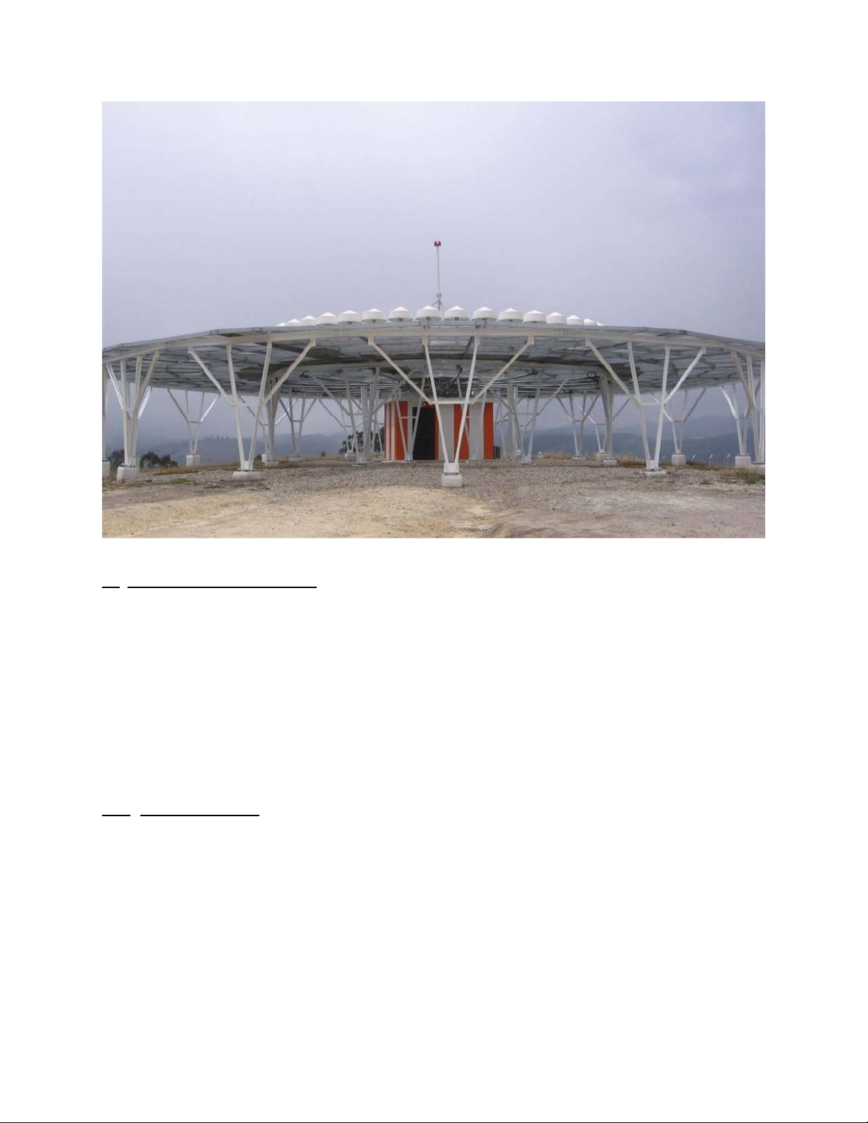
Model 1150A DVOR
Figure 1-2 Dual Doppler VHF Om ni-range (DVOR) S tatio n with DME
EQUIPMENT DESCRIPTION
1.2
The DVOR system provides a reference from which aircraft bearing can be determined. To do this, a carrier is
radiated in the 108 to 118 MHz band and modulated by two 30 Hz signals. One amplitude modulates and the other
frequency modulates (also called the reference phase and variable phase signals, respectively) the carrier signal.
This is done in such a way that the phase difference of the 30 Hz signals varies degree for degree with the magnetic
bearing around the VOR station.
The DVOR system consists of one electronics cabinet with sub-assemblies, a Portable Maintenance Data Terminal
(PMDT), one reference (carrier) antenna and 48 sideband antennas installed on a counterpoise, one field monitor
antenna, and interconnecting cables.
The DVOR electronics cabinet standard configuration uses convection cooling. No fans or blowers are installed in
the cabinet.
Electronics Cabinet
1.2.1
The 1150A VOR is contained in one (1) electronics cabinet measuring 24" wide, 24" deep and 72" high. It utilizes a
standard 19" rack configuration with a front panel door that covers and protects the equipment. The Model 1150A is
100% solid-state. Its internal circuitry is contained on plug-in type printed circuit card assemblies (CCAs) and RF
modules.
Refer to Figure 1-3 through Figure 1-6 which show the layout of the various modules within the Model 1150A
VOR cabinet. The paragraphs on the following pages provide a brief description of each of the modules and
its function in the system. Note that the cabinets shown are dual equipment systems. Refer to Figure 2-2 and
Figure 2-3 for the Model 1150A Doppler VOR system block diagram.
1-2 Rev. - November, 2008
This document contains proprietary information and such information may not be disclosed
to others for any purposes without written permission from SELEX Sistemi Integrati Inc.

Model 1150A DVOR
1.2.1.1
Local Control Unit (LCU) (1A1)
The Local Control Unit (LCU) is located in the upper portion of the VOR cabinet and provides station status
information. The LCU provides for Transmitter, Monitor and System setup, monitoring and control. Alarm
indication from the VOR Monitors initiates transfer or VOR shutdown.
1.2.1.2
Synthesizer Assembly (1A3A1, 1A3A11)
The Synthesizer assembly generates three RF signals (carrier, upper and lower sidebands) for the VOR transmitter.
There are three boards in the Synthesizer Assembly. The Carrier board provides the carrier frequency and phase
control capability for the Carrier Amplifier. The sideband board generates upper and lower sideband frequencies for
the Sideband Amplifier Assemblies. The third board (Interface) provides connectivity to the backplane and includes
digital interface circuitry to the Audio Generator and RMS processors.
1.2.1.3
Audio Generator CCA (1A3A2, 1A3A9)
The Audio Generator CCA is responsible for developing and controlling the audio signals, generating the carrier
modulation signals and monitoring and controlling RF power level and phase control signals used in the DVOR. In
addition, DC analog voltages representing different modulation and power levels of the DVOR RF signals are
applied to, and analyzed by, the audio generator to determine carrier power levels, carrier percent modulation,
sideband power levels and VSWR. An on-board micro controller and memory circuitry controls all functions within
the CCA and communication through the serial connection to the RMS CCA.
Rev. - November, 2008
This document contains proprietary information and such information may not be disclosed
to others for any purposes without written permission from SELEX Sistemi Integrati Inc.
1-3
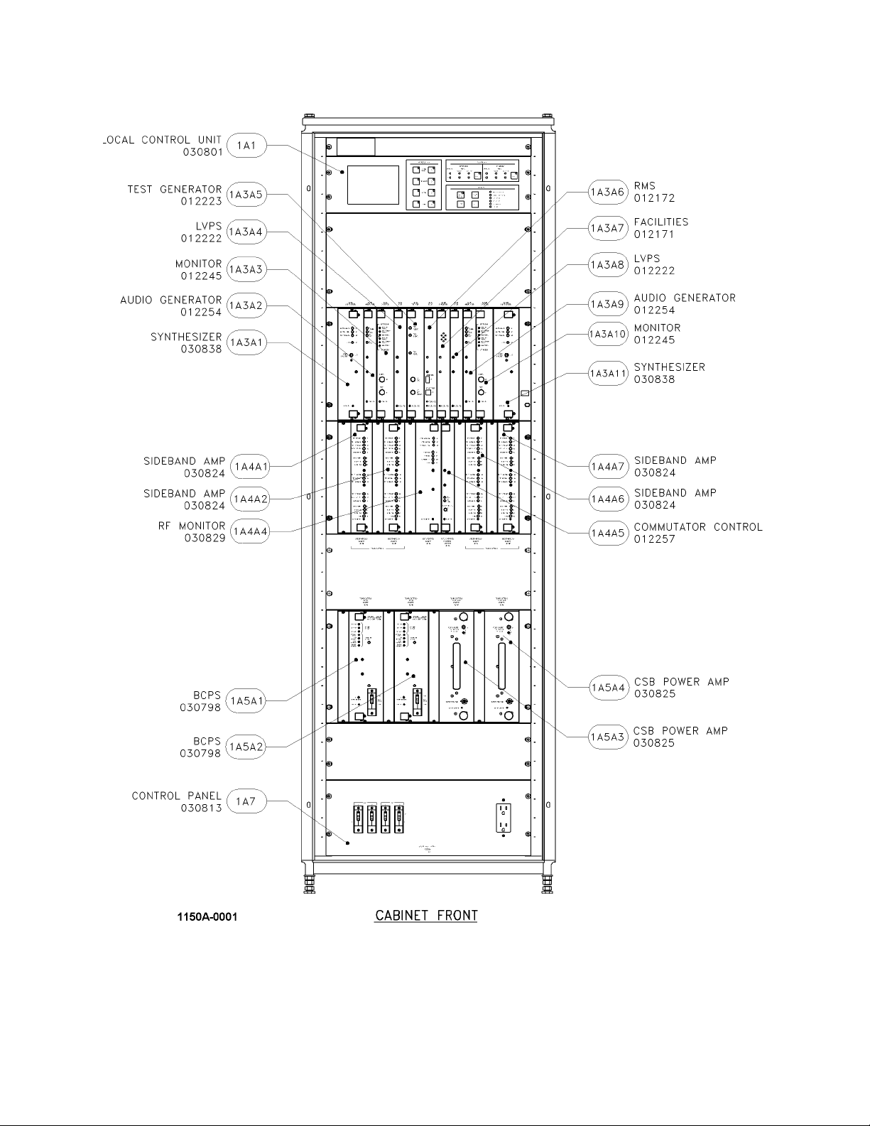
Model 1150A DVOR
Figure 1-3 Location of Major Assemb lies in the Electronics Cabinet (Front Vie w)
1-4 Rev. - November, 2008
This document contains proprietary information and such information may not be disclosed
to others for any purposes without written permission from SELEX Sistemi Integrati Inc.
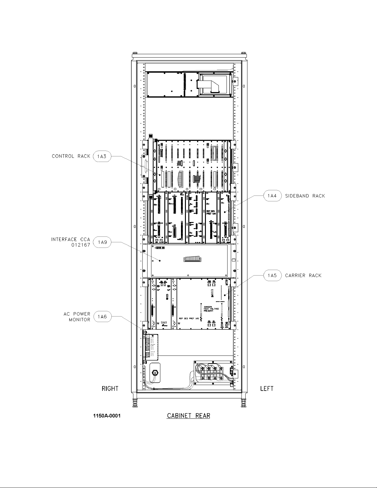
Model 1150A DVOR
Figure 1-4 Location of Major Assembl ies in the Electronics C abinet (Rear View)
Rev. - November, 2008
This document contains proprietary information and such information may not be disclosed
to others for any purposes without written permission from SELEX Sistemi Integrati Inc.
1-5
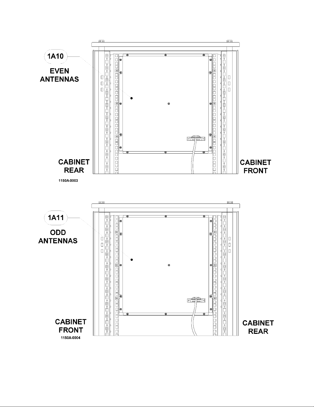
Model 1150A DVOR
Figure 1-5 Location of Commu tator (1A10) A ssemb ly in the E lectronics Cabinet (L eft Si de View)
Figure 1-6 Location of Commutator (1A11) As semb ly in the E lectronics Cabinet (Righ t Si de View)
1-6 Rev. - November, 2008
This document contains proprietary information and such information may not be disclosed
to others for any purposes without written permission from SELEX Sistemi Integrati Inc.

Model 1150A DVOR
1.2.1.4
Monitor CCA (1A3A3, 1A3A10)
The Monitor CCA amplifies the RF input from the field monitor antenna, then band pass filters and analyzes the
signals. The parametric data is displayed on the PMDT and the Monitor CCA initiates an alarm status indication to
the LCU if the DVOR fails to operate within specified limits.
1.2.1.5
Low Voltage Power Supply (LVPS) CCA (1A3A4, 1A3A8)
There are two LVPS assemblies used in the transmitter cabinet. LVPS 1A3A4 is the low voltage power supply for
transmitter 1 and 1A3A8 is the LVPS for transmitter 2. Each LVPS is identical in construction and operation. Each
is interchangeable with the other.
1.2.1.6
Test Generator CCA (1A3A5)
The Test generator CCA performs two functions. Its primary function is to provide a standard reference signal to
the DVOR monitors for calibration whenever directed by the RMS CPU for monitor integrity testing.
The secondary function is an operator maintenance function, which allows test signals to be sent to the monitor(s),
as directed by an operator through the PMDT. The operator can vary signal parameters (i.e., voice band audio
frequency, percent modulation, phase shift, etc.) to determine if a monitor is functioning properly and will alarm at
the required settings.
1.2.1.7
Remote Monitoring System (RMS) Processor CCA ( 1A3A6)
The Remote Monitoring System (RMS) Processor CCA controls the transmitter and monitoring systems. The RMS
CCA performs communications via thirteen serial ports plus a parallel port, and facilitates monitoring/control in a
single or dual VOR system. The RMS CCA receives battery-backed DC power from the BCPS.
The RMS CPU contains a micro controller, RAM, EPROM, EEPROM, bus control and power monitor circuitry. It
processes the system status, directs communications with the outside world, and communicates with the DVOR
monitor and audio generator assemblies.
1.2.1.8
Facilities CCA (1A3A7)
The Facilities CCA provides system I/O for the Remote Monitoring System CCA. Many of the inputs and outputs of
the Facilities CCA eventually connect to the Interface CCA after routing through the Control Backplane CCA.
System battery-backed power supplies (nominally 48VDC) enter and are regulated down into several lower
voltages; including +24V, ±15VDC, ±12VDC, +5VDC, and +3.3VDC.
1.2.1.9
Sideband Amplifier Assembly (1A4A1, 1A4A2, 1A4A6, 1A4A7)
The Sideband Amplifier Assemblies are located in the middle rack (1A4) of the DVOR cabinet. Each Sideband
Amplifier contains one CCA and generates two separate RF signals. Both signals are either above the carrier
frequency or below the carrier frequency by 9960 Hz.
1.2.1.10
RF Monitor Assembly (1A4A4)
The RF Monitor assembly is located in the middle rack (1A4) of the DVOR cabinet. The RF monitor assembly
functions as an RF detector/amplifier and distributor of the detected RF signals. The RF monitor assembly has a
high power dummy load for the carrier mounted to a heat sink that is attached to the assembly chassis. There are
four sideband dummy loads.
1.2.1.11
Commutator Control CCA (1A4A5)
The Commutator Control CCA connects to a 25 conductor cable on the backplane CCA. This cable
originates from one of the two Audio Generators in the Control rack. The output of the Commutator
Control CCA exits onto the backplane and to two 40-pin connectors that connect to ribbon cable from the
Commutator CCAs.
Capability for the ground performance check of the antennas and commutator switching is provided. This check is
automatic after it has been started by the technician and therefore is called an Automatic Ground Check system.
When started, the Monitor CCA sends a switch position code to the Commutator control CCA via the 25-pin cable
originating at the Control rack.
Rev. - November, 2008
This document contains proprietary information and such information may not be disclosed
to others for any purposes without written permission from SELEX Sistemi Integrati Inc.
1-7

Model 1150A DVOR
The switch positions start at 0 and increment by one until 15. Each position represents 22.5 degrees of antenna
rotation from the nominal position. At each position the Monitor CCA determines the azimuth angle at the Field
Monitor antenna location. From this data the errors are measured and a Fourier Analysis is performed to generate
the display data.
The error as determined during the ground check is analyzed to determine the bias, the duantal error, quadrantal
error and octantal error. The bias error is the average error around the station. The duantal error is sinusoidal with a
rate of one cycle in the 360 degrees around the station. The quandrantal error is sinusoidal with a rate of two cycles
in the 360 degrees around the station. The octantal error is sinusoidal with a rate of four cycles in the 360 degrees
around the station
A 4-pin header on the Commutator Control CCA may be strapped to enable/disable the DVOR automatic groundcheck as desired.
WARNING
Enabling the automatic ground-check test changes the signal in space and will cause unsafe
conditions for aircraft. A notice to airmen (NOTAM) must be issued prior to starting this
1.2.1.12
Battery Charging Power Supply (BCPS) Assembly (1A5A1, 1A5A2)
The BCPS assemblies provide regulated voltage to the transmitter from either the AC input or the batteries. The
BCPS assemblies are located in the third rack. The AC voltage is an input to the BCPS which converts to
approximately 50 Volts DC. The BCPS assemblies are also responsible for charging the batteries when AC is
present.
1.2.1.13
Carrier Power Amplifier Assembly (1A5A3, 1A5A4)
The Carrier Amplifier has one assembly. The Carrier Amplifier circuit card assembly, which is also the module’s
I/O, processes the control signals from the Audio Generator to properly control the desired output RF modulation
and amplitude. This assembly is capable of providing 100 Watts or more of Carrier power at up to 80% AM
modulation.
1.2.1.14
Interface CCA (1A9)
The Interface CCA provides interface connections between the RMS/Facilities/Control Backplane CCAs and the
outside world. Examples include spare analog and digital inputs, spare digital outputs, temperature sensors, smoke
detector, and intrusion sensor. RS232 communications are provided to RCSU and PMDT terminals as well as an
Ethernet module. All signals are protected by transient voltage suppression (TVS) devices on the Interface CCA
before exiting.
1.2.1.15
AC Power Monitor Assembly (1A6)
The AC Power Monitor CCA provides a means for the VOR system to measure the AC current and voltage levels of
the obstruction lights and of the VOR system itself. Provision for operating with a photo switch is incorporated. A
capability to bypass the photo switch for the obstruction lights is provided.
1.2.1.16
Commutator CCA (1A10, 1A11)
Each commutator CCA measures 15-7/8" high and 14-7/8" wide. There are two commutator CCAs installed in the
top of the electronics cabinet. They are located on the upper left and upper right side and may be accessed by
removing the cabinet side panels. The right (viewed from the front) commutator CCA is used to switch the RF
signals to all the odd antennas, and the left commutator CCA drives the even antennas. Each commutator has
twenty-six N type RF connectors and two 37-pin D-shell connectors.
Portable Maintenance Data Terminal (PMDT)
1.2.2
The standard PMDT consists of a laptop computer and is the input/output device for controlling and communicating
with the DVOR system. Station control, adjustment and monitoring functions are available through the computer,
and are accessed via a Windows-based operator interface. An optional external mouse may be used with the laptop
computer for ease in operation. An optional desktop PC is available as a substitute for the standard laptop computer.
Also, an optional printer is available for use with either the laptop or desktop PC.
1-8 Rev. - November, 2008
This document contains proprietary information and such information may not be disclosed
to others for any purposes without written permission from SELEX Sistemi Integrati Inc.

Model 1150A DVOR
Station security control is provided through a three-level password system. Complete access to the system for
djustments and measurements is provided at level 3. Modification of non-critical parameters is available at level 2,
a
and read-only access is available at level 1.
All functions available on the local PMDT are available remotely via a modem and dial-up telephone line to an
optional remote laptop or desktop PC running the PMDT software. Refer to Section 3 on the use of the PMDT.
Transmitting Antenna System
1.2.3
The DVOR antenna system consists of a single carrier antenna assembly at the center of the counterpoise, and 48
sideband antenna assemblies spaced equally in a 44' diameter circle concentric with the carrier antenna assembly.
All antennas are enclosed in small, weatherproof, fiberglass radomes.
1.2.3.1
Carrier Antenna
Refer to Figure 1-7. Carrier Antenna is a single Alford loop on a support plate. The antenna is supported above the
counterpoise by a metal pedestal. This antenna is electrically tuned to the station frequency by means of two large,
air-dielectric capacitors. This antenna is designed to function with a collocated distance measuring equipment
(DME) or tactical air navigation (TACAN) antenna system. When required, a metal pipe passes through the center
of the support plate and center of the antenna. The pipe serves as a conduit for feed lines and cables to a DME or
TACAN antenna and obstruction lights, when installed. When collocated with a TACAN, the antenna is enclosed
within a larger fiberglass shelter called a “walk in” radome. Figure 1-8 depicts the carrier antenna provided for use
without collocated DME or TACAN antennas. The hole through the center is not present and the radome and
pedestal are the same as the sideband antennas.
Rev. - November, 2008
This document contains proprietary information and such information may not be disclosed
to others for any purposes without written permission from SELEX Sistemi Integrati Inc.
1-9
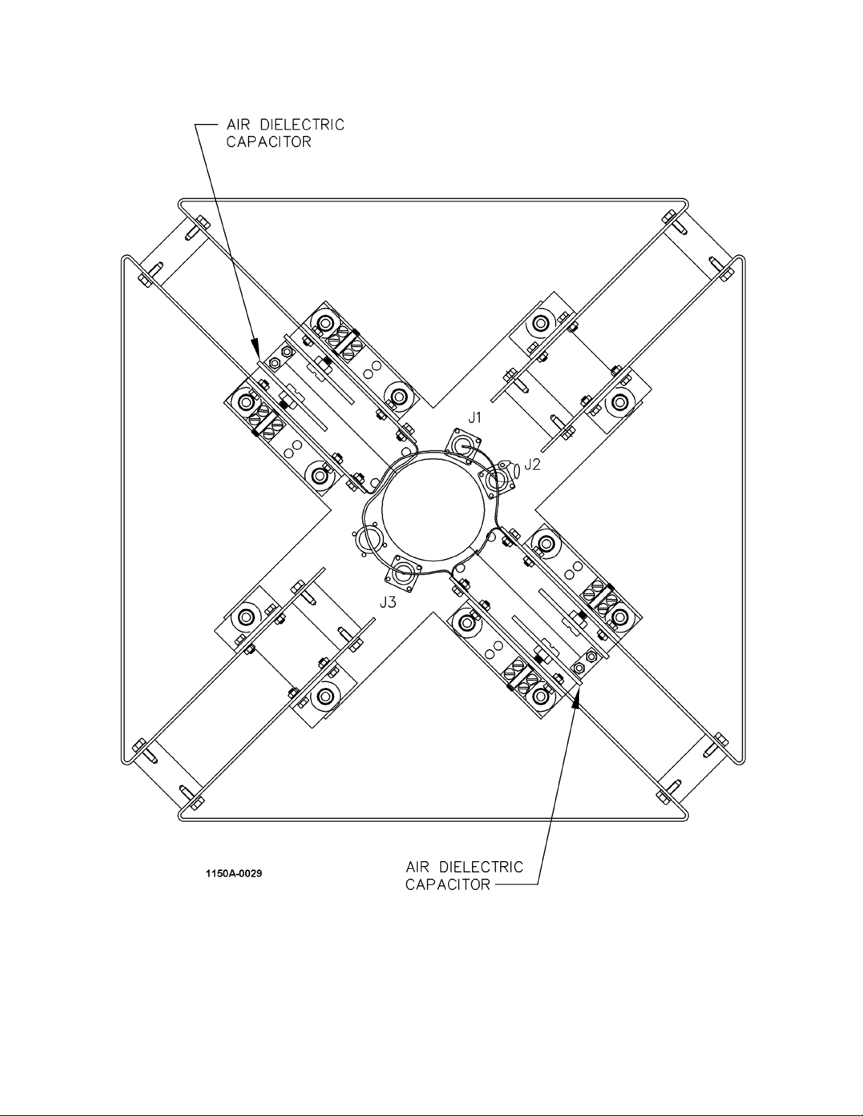
Model 1150A DVOR
Figure 1-7 Carrier Antenna f or coll ocation with DME/TAC AN
1-10 Rev. - November, 2008
This document contains proprietary information and such information may not be disclosed
to others for any purposes without written permission from SELEX Sistemi Integrati Inc.

Model 1150A DVOR
Figure 1-8 Carrier Antenna without DME/TA CAN
Rev. - November, 2008
This document contains proprietary information and such information may not be disclosed
to others for any purposes without written permission from SELEX Sistemi Integrati Inc.
1-11

Model 1150A DVOR
1.2.3.2 Sideband Antenna
Refer to Figure 1-9. Each sideband antenna is an Alford loop, similar to the carrier antenna but without the large
hole in the support plate. This antenna is electrically tuned to the station frequency by means of single high voltage,
glass capacitor. The antennas are mounted independently on individual support plates, supported above the
counterpoise by metal pedestals equal in height to the carrier antenna.
Figure 1-9 Sideband Antenna
1-12 Rev. - November, 2008
This document contains proprietary information and such information may not be disclosed
to others for any purposes without written permission from SELEX Sistemi Integrati Inc.

Model 1150A DVOR
1.2.3.3
Balun
Refer to Figure 1-10. The balun is a line section approximately 180 degrees in length that hangs directly under the
center of the antenna inside the pedestal and is used to develop a balanced signal output from a coaxial line input.
Figure 1-10 Balun, Tunin g Stub, and Pos itioning Piec e
Rev. - November, 2008
This document contains proprietary information and such information may not be disclosed
to others for any purposes without written permission from SELEX Sistemi Integrati Inc.
1-13

Model 1150A DVOR
1.2.3.4 Tuning Stub
Refer to Figure 1-10. The tuning stub is a line section made out of RG-214 cable with a connector on one end and
open at the other end. The function of the stub is to supply the needed capacitive reactance to make the point of the
stub attachment pure resistive.
1.2.3.5
Positioning Piece
Refer to Figure 1-10. The positioning piece is a length of RG-214 cable with a connector at each end. The purpose
of the positioning piece is to place the tuning stub at a point on the input line where the resistive component of the
complex impedance is equal to the characteristic impedance of the line (50 ohms). The length of the positioning
piece is factory selected for the frequency band of operation.
1.2.3.6
Pedestal
Refer to Figure 1-11. The pedestal is a 6061-T6 aluminum tube with mounting plates on each end. The pedestal
supports the Alford loop antenna and provides a conduit for the feed cable, balun, positioning piece, and tuning stub.
1.2.3.7
Radome
Refer to Figure 1-11. The radome is a fiberglass enclosure that protects the radiating elements of the antenna from
the weather and vermin infestation.
Figure 1-11 Antenna Pedestal and Radome Diagram
1-14 Rev. - November, 2008
This document contains proprietary information and such information may not be disclosed
to others for any purposes without written permission from SELEX Sistemi Integrati Inc.

Model 1150A DVOR
Field Monitor Antenna
1.2.4
Refer to Figure 1-12. There are one or two field monitor antennas in each DVOR system. The single dipole antenna
is the standard configuration and two antennas are the optional configuration. A cable from the field monitor
antenna enters a two way power splitter in the VOR transmitter cabinet. The two outputs from the power splitter are
connected to the two Monitor CCAs. The antenna is installed on a support tower 300 to 360 feet from the carrier
antenna. The monitor antenna may be installed on any radial.
Figure 1-12 DVOR Field Monitor Di pole Anten na
1.2.5
Counterpoise
The counterpoise is a circular, metallic support structure upon which the transmitting antenna system is installed.
The counterpoise typically is between 60 and 100 feet in diameter, 8 to 12 feet above ground level. It can be
aluminum or galvanized steel and is assembled of segments bolted together.
Rev. - November, 2008
This document contains proprietary information and such information may not be disclosed
to others for any purposes without written permission from SELEX Sistemi Integrati Inc.
1-15

Model 1150A DVOR
1.2.6 Equipment Shelter
The electronic part of the DVOR (transmitter cabinet and commutator rack) is housed in a shelter environmentallycontrolled with heating, cooling and ventilation. Normally, the shelter is installed below the counterpoise and
directly underneath the carrier antenna.
Battery Backup Unit (Optional)
1.2.7
The battery backup supply contains two battery boxes each containing two lead-acid maintenance-free batteries in a
48VDC configuration. Additional backup capacity can be achieved by adding additional groups of four batteries.
EQUIPMENT SPECIFICATION DATA
1.3
Equipment specifications are listed in Table 1-1.
1.3.1
Transmitter and Antenna System
1.3.1.1 Transmitter
Table 1-1 DVOR Equipment Specifi cations (Transmitter)
Parameter Specification
Carrier Frequency Range: 108 to 118 MHz with 50 kHz channel spacing.
Frequency Control: Synthesizer
Carrier Frequency Tolerance: ±0.0005% (5 PPM)
Carrier Output Power: Transmitter output power adjustable from 25 to 100 Watts (14 to 20 dBW) in 1
Watt increments
Effective Radiated Power: 23 dBW minimum with a transmitter output of 100 Watts
Carrier Level Shift: less than 0.5% for modulation depth up to 80%
Duty Cycle: Continuous
Spurious Outputs: greater than 77 dB below the carrier at 30% modulation
Harmonic Radiation: Meets or exceeds U.S. FCC requirements. Harmonics of 9960 Hz meet or
exceed:
Second harmonic >30 dB lower than fundamental
Third harmonic >50 dB lower than fundamental
Fourth and higher harmonics >60 dB lower than fundamental
Hum and Noise: With voice, VOR reference and identification inputs, hum and noise on the
carrier are more than 30 dB below the audio level equivalent of 30%
modulation.
Maximum Range: Line-of-sight, 175 nautical miles at 37,500 feet (11,433 M) above the facility.
Accuracy: When site meets requirements of ICAO, bearing information on the
horizontally-polarized radiation is within ±1.0° (at a distance of approximately
1000 feet (300 meters) for all elevation angles between 0 and 60 degrees,
measured from the center of the VOR antenna.
1-16 Rev. - November, 2008
This document contains proprietary information and such information may not be disclosed
to others for any purposes without written permission from SELEX Sistemi Integrati Inc.

Table 1-1 DVOR Equipment Specifi cations (Transmitter)
Parameter Specification
Reference Phase Signal (30 Hz AM)
Frequency: 30 Hz ±0.01%
Modulation Depth: 30% Nominal, 0 to 40% digitally controlled
Variable Phase Signal (30 Hz FM)
Frequency: 30 Hz ±0.01%
Sub-Carrier Signal (9960 Hz FM)
Center Frequency: 9960 Hz ± 0.1%
Deviation Ratio: 16 ±1 at 115 MHz (based on 44 ft diameter of sideband antennas)
Modulation Depth: 30% Nominal, 0 to 50% digitally controlled
Identification Signal
Keyer Type: Solid State
Frequency: 1020 Hz ± 0.01 Hz
Modulation Depth: 0 to 20%, adjustable
Harmonic Distortion: less than 1.0%
Code: 2,3,4 letters in Morse Code
Rate: 8 words per minute
Repetition: 4 times/30 seconds; 3 times with co-located DME
Model 1150A DVOR
Voice
Frequency: 300 to 3000 Hz
Modulation Depth: 0 to 30%, adjustable
Harmonic Distortion: less than 1%
Input Level: -30 dBm to +2 dBm
Environmental
Operating Temperature
Indoor Equipment: -10° to +55°
Outdoor Equipment: -50° C to +70°
Relative Humidity
Indoor Equipment: 95% (non-condensing) at +50° C.
Outdoor Equipment: 100% at +70° C
Wind More than 100 mph (85 knots) (160Km/hr) with shelter and counterpoise on
concrete foundation
Ice and Snow 5cm (2 in.) Ice coating causes negligible course error
Altitude 0 to 4500m (0 to 15,000 ft.)
Rev. - November, 2008
This document contains proprietary information and such information may not be disclosed
to others for any purposes without written permission from SELEX Sistemi Integrati Inc.
1-17

Model 1150A DVOR
1.3.1.2 Antenna System
Table 1-2 DVOR Equipment Specifi cations (Anten na Syste m)
Parameter Specification
Type: Alford loop
Frequency Range: 108 to 118 MHz, field-tunable
Polarization: Horizontal
Antenna System Bearing Error: less than 0.5°
DME Co-Location: Permits coaxial mounting of DME antenna above carrier
Weather Protection Fiberglass radome
Blending Function: COS
.836
X
Number of Antenna: 48 Sideband, 1 Carrier
Modulation Type: Double-Sideband
Commutator Type: Solid-State
Frequency Range: 108-118 MHz broadband, no tuning
Blocking Attenuation (Switches Off) Greater than 80 dB
Insertion Loss: 0.5 dB maximum
Difference in Insertion Loss: Less than .05 dB
Phase Balance Less than 2 degrees
VSWR: Less than 1.15:1
Lightning Protection Provided on each Commutator output
1.3.1.3 Field Monitor
Table 1-3 DVOR Equipment Specifi cations (Field Monitor )
Parameter Specification
Antenna Type: Dipole
Number of Antennas: 1 Standard, 2 Optional
Frequency Range: 108 to 118 MHz
Output: Composite VOR signal, RF
Installation: Located at minimum of 91.4m (300 ft) from center of counterpoise
and level with counterpoise
Position: Any azimuth angle
VSWR: U 1.5:1 at 112 MHz
1-18 Rev. - November, 2008
This document contains proprietary information and such information may not be disclosed
to others for any purposes without written permission from SELEX Sistemi Integrati Inc.

Model 1150A DVOR
Monitor
1.3.2
Table 1-4 DVOR Equipment Specifi cations ( Monitor)
Parameter Specification
Configuration: Dual (“And”, “Or” user selectable)
Azimuth Measurement Resolution: ±0.01°
Azimuth Measurement Range: 0 to 360°
Azimuth Measurement Accuracy: ±0.02°
Azimuth Readout Indication: Digital, on the Local Touch Screen display and on the station computer
(PMDT)
Phase Shift Control: Calibrated against test generator
Monitoring of VOR Signal: At any desired azimuth angle
Adjacent Channel Rejection > 50 dB
Monitor Limits
Bearing: 0.1 to ± 5° from any radial, 0 to 360°
30Hz AM Amplitude: ±2% from 30% nominal, adjustable, 21 to 39%
30Hz FM Amplitude: ±2 from nominal ratio 16, adjustable, 12.6-19.4 (ratio)
9960 Hz Subcarrier Amplitude: ±2% from 30% nominal, adjustable, 21 to 39%
Level Alarm: ±3 dB from nominal carrier power, adjustable ±9 dB from nominal
Identification: Incorrect code, lack of ident, continuous ident, or level change of ±3%
Stability of Alarms
Phase Shift: better than ±0.1°
Amplitude: better than ±0.1%
Alarm Time Delay: Adjustable, 4-99 seconds
VSWR Measurement: Continuous measurement and display of individual sideband antenna
VSWR. Maintenance alert if limit exceeded.
VSWR Alarm Limit: 1.0 to 3.0:1
Notch Monitor 50% from reference value, adjustable 0 to 100% nominal
Rev. - November, 2008
This document contains proprietary information and such information may not be disclosed
to others for any purposes without written permission from SELEX Sistemi Integrati Inc.
1-19

Model 1150A DVOR
1.3.3 Mechanical and Electrical
Table 1-5 DVOR Equipment Specifi cations ( Mechanical and El ectrical)
Parameter Specification
Size of Cabinet: 72" H x 24" W x 24" D (183cm H x 61cm W x 61cm D)
Weight of Cabinet: 450 lb (205 kg) maximum
Mounting Floor mount
Primary Power: 85 to 264 VAC, 47 to 63Hz, single phase
Standby Power: Standard 48 VDC no-break battery backup system (four 12V-65Ah batteries)
with charger provides approximately 4.0 hours of operation.
Optional 48VDC no-break battery backup system (four 12V-100Ah batteries)
with charger provides approximately 6.0 hours of operation.
Power Consumption: Single Stations: 375VA (typical), 625 VA with maximum battery charging.
Dual Stations: 500VA (typical), 750VA with standby transmitter operating
for test purposes.
Duty Cycle: Continuous
1.3.4 Remote Control System
1.3.4.1 Design Features
The optional remote control system consists of a Model 2238 or Model 2240 Remote Control and Status Unit
(RSCU) and one Remote Slave Unit (RSU). The 2238 RCSU is designed for installation in a standard 13.33 cm
(5.25") rack panel space in a Control Tower Equipment Room. The 2240 RCSU is designed for installation in a
standard 6.66 cm (2.12") rack panel space in a Control Tower Equipment Room and the RSU’s are designed for
installation at a controllers’ position in the Tower Cab. The 2238 RCSU contains provisions for six ILS Localizer,
Glideslope, Outer Marker and Middle Marker and DME and VOR stations. The 2240 RCSU contains provisions for
up to three ILS Localizer, Glideslope, Outer Marker, Middle Marker, DME, or VOR stations. Each of the respective
stations is connected to the RCSU by an RF data link or a single dedicated telephone line pair. The RSU is then
slaved to the RCSU by interconnecting cables.
1-20 Rev. - November, 2008
This document contains proprietary information and such information may not be disclosed
to others for any purposes without written permission from SELEX Sistemi Integrati Inc.

Model 1150A DVOR
1.3.4.2
RCSU Controls and Indicators
Table 1-6 RCSU Controls and In dicators
Indicators Controls
Main On System On/Off
Standby On System Transfer
Off RMS Reset
Maintenance Alert
System on Batteries
Primary AC Power Fail
System on Local Control
Monitor #1 & #2
Normal
Alarm
Bypass
Monitor Mismatch
Aux Equipment On/Off
Comm Fail
Low Volume RSCU Alarm Silence
Audible Alarms Lamp Test
Control Functions/Indicators for Associated RSU
Operational Status
RSU Module Power Status
Comm Failure w/RSU Module
Common on RCSU
I/O Status & Control
Volume Controls
1.3.4.3 RSU Controls and Indicators
Indicators Controls
VOR System Alarm Silence/Cancel
Main On Alarm Volume Up/Down
Main Alarm/Off Self Test
Standby On Lamp Intensity Up/Down
Standby Alarm/Off
Maintenance Alert
DME System (Co-Located w/VOR)
Main On
Main Alarm/Off
Standby On
Standby Alarm/Off
Maintenance Alert
Aux 1 On/Off
Aux 2 On/Off
RSU AC Power Ok/On Batteries (when optional
Battery Backup is installed)
RSU Communications Failure
Audible Alarm
Table 1-7 RSU Controls and In dicators
Rev. - November, 2008
This document contains proprietary information and such information may not be disclosed
to others for any purposes without written permission from SELEX Sistemi Integrati Inc.
1-21

Model 1150A DVOR
1.3.5 Remote Maintenance Monitoring System (RMM)
1.3.5.1 Design Features
The Remote Maintenance Monitoring (RMM) system operates in conjunction with the local control system and
Portable Maintenance Data Terminal (PMDT). The RMM is an integral part of the DVOR system and consists of
the various embedded sensors, internal monitoring points, microcomputers and built-in test equipment to remotely
monitor, control, record and certify proper operation of the system.
The RMM system is accessed locally through the built-in RS-232 port, and remotely through a dial-up telephone
line, fiber optic line, radio link or GSM telephone connection, and a Portable Maintenance Data Terminal (PMDT).
The telephone line, fiber optic line, radio link, or GSM telephone connections are all optional. The choice of which
communication system is to be utilized for a particular installation, and who is to supply it, is determined by
individual contract.
In addition, the Remote Control and Status Unit (RCSU) computer and modem may be utilized for dial-up access to
the RMM system.
1.3.5.2
RMM Functions
The RMM system provides the following key functions:
a. System control.
b. Adjustment of transmitting parameters.
c. Monitoring of system performance and certification parameters. Compares the outputs of each of the
monitoring devices at least once per second to determine alarm and alert status by comparing the monitored
values to pre-determined limits.
d. Adjustment of all alarm and alert monitoring limits.
e. Monitor Certification through the system test generator.
f. Storage of monitor alert and alarm data, control settings, operational parameters and limits, initialization
data, data files and fault history locally within the RMS. Storage of parameters is backed by either lithium
battery or EEPROM for a non-volatility of 90 days or greater. DVOR parameters may be stored to and
retrieved from the PMDT for a permanent record.
g. System Fault Diagnostic routines with result reporting and storage in memory. “On-Air” diagnostic
routines may be initiated either locally at the station or remotely. By default, diagnostic routines which
require the station to be NOTAMed out of service must be run locally. The station may be user reconfigured, if desired, to allow all diagnostic routines to be run from a remote location.
h. Monitoring of routine maintenance parameters including voltages and currents and antenna VSWR.
i. Monitoring of environmental parameters (when optional sensors are installed).
j. Monitoring the presence or absence of Primary AC Power applied to the system.
k. Printing of menus and all display/parameter values (when optional printer is supplied).
l. Provide clock calendar function within the RMS. The display is date, hours, minutes and seconds. The
current time and date may be set from the PMDT. The RCSU provides the master clock update at periodic
intervals. The accuracy is to within 15 seconds per month and retains the clock/calendar function even
when power is lost by the use of a lithium battery. The lithium battery can maintain the operation of the
clock for up to 180 days.
m. Provide building security monitoring (optional). For this system, an intrusion sensor is installed on the
DVOR equipment shelter door. If the door is open longer than 0.25 seconds, and the security feature has
not been bypassed through the PMDT within a programmable period of 0 to 5 minutes, an alarm message is
generated. Disconnecting the PMDT starts a 0 to 30 minute programmable timer before the intrusion
sensor is reset. The default settings are 5 minutes for the bypass period and 30 minutes for the reset period.
Activation, disabling, reset and bypass of the Intrusion sensor is supported both locally and remotely.
n. Provide monitoring of an optional ionization type smoke detector. Detection of smoke generates an alarm
message.
1-22 Rev. - November, 2008
This document contains proprietary information and such information may not be disclosed
to others for any purposes without written permission from SELEX Sistemi Integrati Inc.

1.4 EQUIPMENT AND ACCESSORIES SUPPLIED
Table 1-8 is a list of all major equipment and accessories supplied.
Table 1-8 Equipment and Access ories Su pplie d
Quantity Nomenclature
Unit
Number
1 Electronics Cabinet 1
Model 1150A DVOR
Dimensions
(in inches)
72" H x 24" W x 24" D
(183cm H x 61cm W x 61cm D)
Weight
450 lbs
(205kgs)
49 Transmitting Antennas E1 thru E49 20.25"W x 20.25"D x 5.5"H each
1 Field Monitor Antenna 4
Prior to assembly:
5.5"W x 13"D x 6.5"H
13 lbs
(5.9 kgs)
20 lbs
(9.1 kgs)
1 Portable Terminal (PMDT) 3
Consisting of:
IBM Compatible laptop
computer
13"W x 13.25"D x 3"H
10 lbs
(4.5 kgs)
PMDT Software
1
Battery Backup System
(12V-65Ah)
36"H x 18" W x 18" D
231 lbs
(105kgs)
1.5 OPTIONAL EQUIPMENT
Table 1-9 and Table 1-10 contain a list of optional equipment that can expand the capabilities of the VOR system or
aid a technician in maintenance and troubleshooting.
Equivalent test equipment can be substituted for that recommended.
Table 1-9 Optional Test Eq uipment
Quantity Nomenclature Part No.
1 Oscilloscope 950259-0000
Oscilloscope; Dual Trace, BW V 25 MHz
Delayed Sweep
1 Frequency Counter 950260-0000
1 RF Wattmeter 950258-0000, Bird Model 43
1 5-W Wattmeter Element 950552-0301, Bird 5B
1 100-W Wattmeter Element 950552-0405, Bird 100C
1 250-W Wattmeter Element
950552-0306, Bird 250B or
950552-0406, Bird 250C
1 RF Sampler Element 950262-0000, Bird 4274-025
1 Digital Multi-meter 950257-0000
3-1/2 Digit
1 Torque Wrench 399003-0000
(For SMA RF Connectors)
1 Adapter, BNC Female to Phone 180218-0000
2 Dummy Load, 5-Watt, Type N-Male 950270-0000, Bird 5-T-MN
Rev. - November, 2008
This document contains proprietary information and such information may not be disclosed
to others for any purposes without written permission from SELEX Sistemi Integrati Inc.
1-23

Model 1150A DVOR
Quantity Nomenclature Part No.
1 Battery Backup System 12V-100Ah 470639-0003
1 Environmental Sensors (Smoke, Temperature, Intrusion) 470357-0003
1 Extender Cables 470449-0001
1 Wattmeter Bodies Kit 470451-0001
1 Field Monitor
1 Printer – Universal AC Input 950311-0003
Table 1-10 Optional Station Equipment
Obstruction Lighting
Incandescent - 120V 470630-0001
- 240V 470630-0002
LED - 120V 470630-0003
- 240V 470630-0004
1-24 Rev. - November, 2008
This document contains proprietary information and such information may not be disclosed
to others for any purposes without written permission from SELEX Sistemi Integrati Inc.

Model 1150A DVOR
ECHNICAL DESCRIPTION
2 T
INTRODUCTION
2.1
The Model 1150A DVOR system is a dual transmitter system, with dual monitoring facilities. It is designed for
terminal and en route navaid operation. The VOR is identified by a specifically assigned two to four letter Morse
code identity and may also include voice identification. In addition automatic terminal information service (ATIS)
information may be modulated onto the VOR signal with a standard input connection. The DVOR can be collocated
with DME to provide distance information in addition to bearing data.
The DVOR concept is based on the 360° radials which originate from a transmitting station and on the airborne
equipment which resolves the particular radial data from the station. The resolved radial, called line-of-position
(LOP) is the displacement angle between magnetic north and the aircraft, as measured from the DVOR antenna.
Therefore, regardless of its heading, an aircraft which is on the 0° radial is north of the DVOR station. The
magnetic course to the station is the reciprocal of the radial. In addition, to/from orientation data, relative to the
DVOR station, is also resolved by the airborne equipment.
OPERATING PRINCIPLES
2.2
Operation of the DVOR is based on the phase difference between two 30 Hz signals modulated on the carrier, called
the reference phase and the variable phase.
The reference phase signal is obtained by amplitude modulating the carrier with a 30 Hz sine wave signal. This
amplitude modulated (AM) signal is radiated omni-directionally in the horizontal plane by the central, carrier
antenna. The radiation pattern is a circle, and produces in the aircraft receiver a 30 Hz signal with a phase
independent of azimuth.
NOTE
DVOR system requires separately radiated upper and lower sideband frequencies which are
displaced ±9960 Hz from the carrier frequency. The Model 1150A DVOR has synthesizer
controlled frequencies which are assigned as follows: carrier (on-channel) station frequency,
carrier frequency plus 9960 Hz, carrier frequency minus 9960 Hz.
The variable phase signal is obtained from the 9960 Hz frequency modulated subcarrier which amplitude modulates
the carrier. This amplitude modulation of the carrier is often referred to as the space modulation, since it is obtained
by adding in space the omni-directionally radiated carrier and the separately radiated upper and lower sideband
signals emanating from the ring of sideband antennas. The upper and lower sideband signals are displaced, on
average, 9960 Hz above and below the carrier respectively and, when added in correct phase to the carrier, will
produce a resultant signal which is amplitude modulated at 9960 Hz.
The subcarrier is frequency modulated at a 30 Hz rate. The sideband signals are sequentially distributed to and
radiated from the 48 sideband antennas in such a way as to simulate two diametrically opposed antennas, rotating
counterclockwise about the circumference of the sideband antenna ring at 30 revolutions per second, with one
antenna radiating the upper sideband signal and the other the lower sideband signal. Since the effective length of the
path of travel between the rotating sideband sources and the distant point of reception varies at a 30 Hz rate, the
observed frequency of the sideband signals varies also at a 30 Hz rate (i.e., the sidebands) and therefore, the
subcarrier is frequency modulated at 30 Hz.
The amount of frequency deviation is proportional to the diameter of the sideband antenna ring expressed in
wavelengths at the operating frequency. Setting the diameter to 44.0 feet (13.4 meters) produces peak frequency
deviation of 480 Hz at a frequency of 113.85 MHz, 454 Hz at 108 MHz and 497 Hz at 118 MHz. Figure 2-1 depicts
a typical RF spectrum of a DVOR with an operating frequency of f
. The corresponding deviation ratio varies
c
therefore from 15.13 at 108 MHz to 16.57 at 118 MHz.
Rev. - November, 2008
This document contains proprietary information and such information may not be disclosed
to others for any purposes without written permission from SELEX Sistemi Integrati Inc.
2-1

Model 1150A DVOR
Figure 2-1 RF Spectrum of a Doppler VOR
The deviation frequency is determined by the formula:
xx=
Where: f
equals the deviation frequency in hertz.
d
f
d
W equals the angular velocity of the signal (30 Hz).
X equals the diameter of the ring in wavelengths.
Y equals 3.14.
f
d
=
r
d
30
In the aircraft receiver, a 30 Hz signal is extracted from the 9960 Hz FM subcarrier. The phase of this second 30 Hz
signal varies linearly with the change of the azimuth bearing of the receiving point; for each degree of azimuth
change, the phase of the 30 Hz variable phase signal changes by one degree.
2-2 Rev. - November, 2008
This document contains proprietary information and such information may not be disclosed
to others for any purposes without written permission from SELEX Sistemi Integrati Inc.

Model 1150A DVOR
The sequential energizing of the sideband antennas and the 30 Hz amplitude modulation of the carrier are time
elated in such a way that the reference and the variable phase 30 Hz signals are in phase at zero degrees (0)
r
magnetic from the DVOR station. As the receiving point is moved clockwise around the station, the variable phase
signal (30 Hz FM) begins to lead the reference signal (30 Hz AM). For example, for the observer west of the
DVOR, the 30 Hz FM signal leads the 30 Hz AM signal by 270 degrees. The aircraft receiver determines the phase
difference between the two 30 Hz signals and thus it’s bearing in degrees (magnetic), relative to the station, as the
number of degrees by which the 30 Hz AM signal lags the 30 Hz FM signal.
DVOR Antenna Principles
2.2.1
The DVOR antenna system simulates a rotating arm with a transmitting antenna at each end, radiating the upper
sideband signal from one end and the lower sideband signal from the other end. This is achieved electronically by
using 48 antennas spaced equally around the perimeter of a circle 44 feet (13.4 meters) in diameter, with an antenna
in the center of the circle radiating a reference carrier.
Consider the effect of simulated antenna rotation on an airborne receiver. When the upper sideband source is
moving toward the aircraft, the Doppler effect causes the airborne receiver input frequency to become higher than
fc+9960 Hz, and for the lower sideband source, which is moving away, the frequency becomes less than fc±9960
Hz, fc being the carrier frequency. The frequency difference changes sinusoidally due to the simulated rotation.
The difference is at a maximum when the line joining the two radiating antennas is perpendicular to the radial to the
aircraft. The difference is equal to zero when the two sideband sources align with the radial to the aircraft since, at
that moment, the distance between each sideband source and the receiver does not vary.
The moment of zero frequency deviation is different for different positions of the aircraft around the station.
Therefore, the recovered 30 Hz FM signal will have a different phase for each of these different positions. For the
receiver North of the DVOR station, the 30 Hz FM signal must be in phase with the 30 Hz AM signal; both signals
passing through their positive zero crossings at the same time. To achieve this, the following has to be observed: At
the moment that the 30 Hz amplitude modulation of the carrier is passing through its positive zero crossing, the
simulated rotating antennas shall align with antenna number 1 (at North) and antenna number 25 (at South), with the
North antenna radiating the peak of the lower sideband signal and the South antenna radiating the peak of the upper
sideband signal. The lower sideband frequency will be decreasing; the upper increasing. The subcarrier frequency
will be increasing from exactly 9960 Hz up and the 30 Hz FM signal will be passing through its positive zero
crossing.
DVOR TRANSMITTER THEORY OF OPERATION
2.3
The following paragraphs provide a technical description of the Model 1150A DVOR, its individual components
and accessories. Refer to Figure 2-2 for simplified block diagram of the DVOR Transmitter System and Figure 2-3
for a detailed block diagram of the DVOR system.
Simplified System Block Diagram
2.3.1
Refer to Figure 2-2. The transmitter (main and standby) consists of a frequency synthesizer assembly, CSB power
amplifier assembly, directional coupler, audio generator CCA, and two sideband generators,
The frequency synthesizer assembly produces the three interrelated RF signals used by the DVOR. The on- channel
carrier RF signal drives the CSB power amplifier assembly. The upper and lower sideband RF signals drive the two
sideband generator assemblies.
The CSB power amplifier assembly amplifies and modulates the carrier RF signal to the operational output level.
The CSB power amplifier also provides a sample portion of the RF energy to be used as an error correction that is
sent back (feedback) to the frequency synthesizer assembly.
The bi-directional coupler obtains a sample of the forward and reflected RF carrier power. The sampled forward
and reflected power is directed to the RF monitor assembly where the signal is used in the detection and analysis
process circuitry.
Rev. - November, 2008
This document contains proprietary information and such information may not be disclosed
to others for any purposes without written permission from SELEX Sistemi Integrati Inc.
2-3

Model 1150A DVOR
The RF monitor assembly functions as an RF detector/amplifier and distributor of the detected RF signals. The
assembly also contains the dummy load for the standby transmitter carrier RF signal. The RF Monitor includes builtin dummy loads for the four sideband signals.
The Audio Generator CCA generates and processes all of the modulation signals transmitted by a DVOR transmitter
and generates the power level and phase control signals needed to operate the transmitter and commutator. It is also
responsible for monitoring the operational status of the transmitter.
The DVOR system uses two sideband generator assemblies for each transmitter. Each sideband generator contains
one Sideband Generator CCA.
The Sideband Generator amplifies the CW RF signal from the frequency synthesizer to the operational output power
levels.
Field
-50 to +10 dBm
Monitor
Antenna
MONITOR MONITOR
PMDT
CO-LOCATED
DME / TACAN
RCSU
Current Data, Settings
Keying, RMM
Remote Control
Indication
RMS
INTERFACE
CIRCUIT
CARD
Alarm
Current Data, Settings
VOR
Status
Restart
BCPS1
LOCAL
CONTROL
UNIT
(LCU)
LV
PS
Alarm
Indication
Synth Disable
Audio Modulation
Disable
+28
+12
-12
+5
BCPS2
LV
PS
+28
+12
-12
+5
Figure 2-2 Simplified DVOR C ontrol and Monitorin g Block Di agram
2-4 Rev. - November, 2008
This document contains proprietary information and such information may not be disclosed
to others for any purposes without written permission from SELEX Sistemi Integrati Inc.

Model 1150A DVOR
Carrier Antenna
RS422 Control Signals
Modulation
RF Monitor
COMMUTATOR
CONTROLLER
SIDEBAND
4
SIDEBAND
3
SIDEBAND
2
SIDEBAND
1
RF
SWITCH
RF
SWITCH
RF
SWITCH
RF
SWITCH
Bank4
Bank3
Bank2
Bank1
To Sideband
SIDEBAND
4
SIDEBAND
3
SIDEBAND
2
SIDEBAND
1
48 Cables
Antennas
Modulation
CW (0 dBm)
30 dB
CW
(0 dBm)
30 dB
SYNTH
CARRIER
AMP
AUDIO
GENERATOR
RF
SWITCH
SERIAL DATA TO RMS
SERIAL DATA TO RMS
CARRIER
AMP
SYNTH
AUDIO
GENERATOR
Figure 2-3 Simplified DVOR T ransm itter Block D iagram
Rev. - November, 2008
This document contains proprietary information and such information may not be disclosed
to others for any purposes without written permission from SELEX Sistemi Integrati Inc.
2-5

Model 1150A DVOR
Refer to Figure 2-3. The Remote Maintenance System Processor (RMS) handles all command, control,
communications and information for the DVOR system.
A monitor antenna located on any radial in the far field provides an RF signal which is equally divided and sent to
the VOR monitors for processing and analysis.
The VOR monitor CCA works independently from the transmitter and from each other; however, the alarm control
features of both monitors can be organized to function in a logical AND or logical OR arrangement.
The Local Control Unit (LCU) is responsible for turning off the transmitters and transferring from Main to Standby
transmitters. The LCU contains hardware logic that acts on alarm inputs from the Monitors. The LCU has two
controls to each transmitter to remove radiation in case of out-of-tolerance conditions. The LCU is responsible for
controlling the transfer relays and reporting the current state of the relays as to which transmitter is connected to the
antenna.
The transmitter cabinet contains the assemblies needed to control the electronic switching of the sideband antennas.
2.3.1.1
Electronics Cabinet (Unit 1)
The VOR electronics cabinet assembly contains all of the electronic assemblies that generate, control, and monitor
the DVOR modulated radio frequencies. The cabinet contains three separate card cage assemblies that hold the
transmitter and RMS modules. It provides the means to physically secure the modules within the electronics cabinet
and provides for the interconnection of the modules. Attached, but independent from it, are the five coaxial latching
relays mounted to the middle card cage directly behind the RF monitor assembly. The relays are latched by
applying a ground pulse to either the latch or release coil. The relays are powered from a common 28 volt source.
The relays switch the ten RF inputs (main and standby) between the antenna system and the dummy loads. They
also provide DC logic signals which are used by the Monitors and Audio Generators to sense which transmitter
system is connected to the antenna system. The DC logic signal is supplied to the Audio Generator to enable
commutator switching signals and identification to be applied from the on-air Audio Generator CCA.
System Block Diagram Theory
2.3.2
Refer to Figure 2-2 and Figure 2-3. The DVOR system block diagram depicts the main components (both optional
and required) of a functional station and identifies primary signal, control and voltage paths within the station.
The DVOR system is contained in an electronics cabinet assembly. Connected to this DVOR cabinet are the
PMDT, carrier antenna, sideband antennas, field monitor antenna, and optional backup batteries.
The electronics cabinet is next broken down into its main components which are a Local Control Unit (LCU), RMS,
main and standby transmitters, VOR monitor CCAs, RF monitor, changeover relays, battery charger power
subsystems (BCPS).
The LCU contains the displays that provide a visual indication of the status of the VOR system along with control to
change the operational states of the DVOR.
The RMS group handles all command, control, communications, and information for the station.
The main transmitter consists of a frequency synthesizer assembly, CSB power amplifier assembly, directional
coupler, audio generator CCA, and two sideband generators. Supplying the voltage for the main transmitter is a
stand-alone battery charger power subsystem, and a Low Voltage Power Supply (LVPS).
The frequency synthesizer assembly contains three CCAs. They are the carrier CCA, the Sideband CCA and the
Interconnect CCA. This assembly produces the three interrelated RF signals used by the DVOR. The on-channel
carrier RF signal drives the CSB power amplifier assembly. The upper and lower sideband RF signals drive the two
sideband generator assemblies.
2-6 Rev. - November, 2008
This document contains proprietary information and such information may not be disclosed
to others for any purposes without written permission from SELEX Sistemi Integrati Inc.

Model 1150A DVOR
The Audio Generator CCA generates the carrier modulation signals, monitors and controls power levels, and directs
he RF phase control signals for the DVOR transmitter.
t
Each sideband generator contains one CCA within the assembly. Functionally, each sideband generator has two
sideband amplifiers on the one sideband amplifier CCA. Each sideband amplifier is designed to amplify and
modulate one of the four individual sideband signals used by the DVOR system.
The CSB power amplifier contains one CCA. The CSB power amplifier assembly amplifies the carrier RF signal to
the operational power level of the station and modulates it with the specified audio signals. A sample of the RF
energy to be used as an error correction feedback signal that is sent to the frequency synthesizer assembly. A second
sample of the RF is provided on the front panel test point on the CSB power amplifier assembly. A directional
coupler in the carrier feed-line allows sampling of the forward and reflected RF energy.
The RF monitor processes the main and standby RF signals for use by the audio generator and VOR monitor CCAs.
The RF monitor contains all the dummy loads, for use by the standby transmitter.
The field monitor antenna cable enters the two way equal power splitter in the cabinet. The outputs of the power
splitter feed each of the two VOR monitors for processing and analysis. Each VOR monitor CCA works
independently from the main transmitter and from each other; however, the alarm control features of both monitors
can be organized to function in a logical AND or logical OR arrangement.
2.3.2.1
Frequency Synthesizer (1A3A1, 1A3A11)
The Synthesizer assembly generates a three RF signals (carrier, upper and lower sidebands) for the VOR transmitter.
There are three boards in the Synthesizer Assembly. The Carrier board provides the carrier frequency (see Table
9-4) and the phase control capability for the Carrier Amplifier. The long term phase is kept constant in the carrier
amplifier by means of a phase control loop in the synthesizer. The phase control loop also removes unwanted phase
modulation in the carrier amplifier due to amplitude modulation.
The sideband board generates the upper and lower sideband frequencies for the Sideband amplifier Assemblies and
provides the ability to adjust the sideband generator phase over 360 degrees relative to the carrier. This eliminates
the need to cut the antenna cables during installation.
2.3.2.1.1
Frequency Synthesizer Block Diagram Theory
Refer to Figure 2-4. The function of the Frequency Synthesizer Assembly is to create the Carrier, Upper Sideband,
and Lower Sideband radio frequencies radiated by the VOR Transmitter. The Synthesizer Assembly is used in both
CVOR and DVOR system configurations. The Synthesizer Assembly generates the Carrier Signal using a
synthesized PLL and control loop to lock the frequency. In addition to the PLL synthesized RF Generator, there is
another phase lock loop in the Synthesizer. This loop is used to maintain the carrier phase relative to the reference
RF signal, and correcting for amplitude modulation induced phase mod on the VOR Carrier Transmitter output
signal. There are three boards (CCAs) in the 030838-0001 Frequency Synthesizer Module, the 012258 Sideband
CCA, the 012262 Interface CCA, and the 012263 Carrier CCA. The majority of the circuitry is located on the
012258 Sideband CCA and the 012263 Carrier CCA; with the test port buffer amplifier and audio generation
circuitry on the 012262 Interface CCA.
There is a temperature compensated crystal oscillator, or TCXO, on the 012262 Interface CCA that generates a
10.000 MHz reference signal. This signal is buffered and divided by 50 to create a 200 KHz loop reference signal
for the carrier PLL. The 10.000 MHz reference signal is also buffered and sent directly to the Direct Digital
Synthesizer (DDS) for processing of the 9960 Hz signal generation.
Rev. - November, 2008
This document contains proprietary information and such information may not be disclosed
to others for any purposes without written permission from SELEX Sistemi Integrati Inc.
2-7

Model 1150A DVOR
Refer to Figure 2-4. The carrier frequency is generated by a PLL synthesizer, referenced to the precision 200 KHz
signal. A voltage controlled oscillator, or VCO, generates the RF signal. This signal is buffered, and a portion of
the signal fed back to the PLL controller, where it is divided by a programmable divider. The divided output is
compared to the precision 200 KHz reference signal in the PLL controller’s phase comparator. The phase
comparator generates an error voltage signal that is filtered and applied to the voltage control input of the VCO, thus
locking the VCO output frequency to the reference. VOR channel selection is accomplished by changing the divide
ratio of the PLL controller’s divider. This divide ratio is programmed into the PLL controller by a serial port
interface (SPI) located in the audio generator CCA. The output of the carrier synthesizer is split and routed to the
carrier phaser, the carrier phase reference, the front panel test port buffer amplifier, and the sideband board in the
synthesizer assembly.
The test port buffer amplifier is located on the 012262 Interface CCA, on the backside of the frequency synthesizer
module. The output of this buffer is attenuated to provide the 10 mW typical carrier frequency output signal
available on the front panel SMA connector. The attenuator also serves to provide a resistive load for the buffer
when no external load is connected to the SMA connector. The 012262 boards serve as an interface with the
Synthesizer (012258) and Carrier (012263) boards to communicate with the system through the backplane. The
012262 board also contains circuitry for sideband generation and power supplies for each of the boards mounted.
The 012258 and the 012263 board each have a 30 pin header for connecting to the 012262 Interface board. The
012258 and 012263 boards are mounted in a housing to provide isolation between the carrier and sideband signals.
PHASE
DETECTOR
DIVIDE BY 50
(200KHz REF)
10 MHz Ref
TCXO
CARRIER
CONTROLLER
AUDIO GENERATOR
SPI BUFFER
From Audio
Generator
LOOP
LOOP FILTER
VCO AND
BUFFERS
CARRIER MEAN
AND DYNAMIC
PHASER
TEST PORT
BUFFER
FREQ/2560
DIVIDER
PHASE
SHIFTER AND
BUFFERS
DIRECT
DIGITAL
SYNTHESIZER
CARRIER
AMPLIFIER
FRONT
PANEL TEST
POINT
CARRIER FREQ
COUNTER
OUTPUT
USB
QUADRATURE
MODULATOR
CVOR/DVOR
MODE
SELECT
LSB
QUADRATURE
MODULATOR
VOR SYSTEM
CARRIER
AMPLIFIER
(EXTERNAL)
USB BUFFER
AMPLIFIER
USB
DETECTOR/
BUFFER
AMPLIFIER
FREQ/2560
DIVIDER
FREQ/2560
DIVIDER
LSB BUFFER
AMPLIFIER
LSB
DETECTOR/
BUFFER
AMPLIFIER
VOR SYSTEM
CARRIER
OUTPUT
USB RF
OUTPUT
USB
DETECTED
OUTPUT
USB FREQ
COUNTER
OUTPUT
LSB FREQ
COUNTER
OUTPUT
LSB RF
OUTPUT
LSB
DETECTED
OUTPUT
Figure 2-4 Synthesizer Block Diagram
2-8 Rev. - November, 2008
This document contains proprietary information and such information may not be disclosed
to others for any purposes without written permission from SELEX Sistemi Integrati Inc.

Model 1150A DVOR
The output of the carrier phaser is amplified by the carrier buffer amplifier, and feeds the high power carrier
mplifier module in the VOR system. In the process of amplitude modulation, the VOR carrier amplifier generates
a
undesired phase modulation of the output signal. In addition, the transfer phase of the RF amplifier chain will drift
due to temperature. The carrier phaser is used to counter both of these effects. Feedback from the VOR carrier
output signal is routed back to the Frequency Synthesizer module. This feedback is representative of the final RF
carrier output signal, and has both the 30 Hz amplitude modulation, and the undesired phase shift information.
This carrier feedback signal is first passed through a limiter in the Frequency Synthesizer module to remove the 30
Hz AM information. The output of the limiter is applied to a phase detector where it is compared to the direct
output of the carrier PLL synthesizer. The output of this phase detector is a phase error signal, which is amplified
and filtered to drive the carrier phaser. The carrier phaser is modulated to maintain the error voltage at zero volts,
hence countering the undesired phase shift and phase modulation effects of the VOR carrier RF amplifier.
There is a DC offset input to the carrier phase error amplifier that has the effect of shifting the phase of the VOR
carrier output signal with respect to the reference phase in the frequency synthesizer module. This allows for phase
adjustment of the carrier to sideband output RF signals to optimize the signal in space characteristics of the VOR
radiated signal.
The carrier frequency counter divider is also programmed by the SPI interface from the audio generator board. It
provides a fixed divide by 2560 CMOS compatible output for carrier frequency monitoring.
In a DVOR system configuration, the upper and lower sideband frequencies are generated in the synthesizer on the
Sideband 012258 CCA. The 012258 CCA derives the upper and lower sideband signals from the carrier signal
using two quadrature modulators. The modulators use the 9960Hz signals from the Direct Digital Synthesizer
(DDS) on the interface board to mix with the carrier signal. Each sideband signal is generated when the In phase (I)
port of the quadrature modulator is 90 degrees out of phase with respect to the quadrature (Q) port of the quadrature
modulator. The upper sideband is generated when the I-port is +90 degrees with respect to the Q-port. The lower
sideband is generated when the I-port is -90 degrees with respect to the Q-port. This allows the upper and lower
sideband signals to always be 9960 Hz offset from the carrier frequency no matter what channel the VOR system is
transmitting on.
In a CVOR configuration, only the lower sideband path is used. The upper sideband quadrature modulator is
disabled and the lower sideband quadrature modulator is configured to pass only the carrier signal without any
frequency offset. This allows only software programming to determine a CVOR/DVOR system configuration using
the same module.
Both the upper and lower sideband PLL synthesizers have fixed divide by 2560 dividers that operate in the same
fashion as the carrier PLL synthesizer to provide for upper and lower sideband frequency monitoring. In addition,
there are detectors on each of the carrier, upper sideband, and lower sideband signals for power detection and
monitoring of the synthesizer assembly.
The synthesizer assembly also contains phase control circuitry to digitally step the phase in 90 degree increments
referenced from the carrier signal for a coarse phase adjustment. A fine adjustment is made with an analog phaser.
The analog phaser is capable of a minimum of +/- 45 degrees of adjustment range. This allows a total adjustment
range of 360 degrees for the sideband signal referenced to the carrier signal and reduces cable cutting to phase the
VOR system.
2.3.2.1.2
Frequency Synthesizer (1A3A1, 1A3A11) Detailed Circuit Theory
2.3.2.1.2.1 Frequency Reference Circuitry
Refer to Figure 11-12. Oscillator Y1 is a temperature compensated crystal oscillator, or TCXO, which provides a
precision 10.000 MHz CMOS compatible signal at its output. Potentiometer R27 is a trim adjustment for Y1 on the
012262 CCA used to make fine adjustments to output frequency and to compensate for possible crystal aging.
Rev. - November, 2008
This document contains proprietary information and such information may not be disclosed
to others for any purposes without written permission from SELEX Sistemi Integrati Inc.
2-9

Model 1150A DVOR
The output of Y1 routes to buffers U15:A and U15:B. The buffer U15:B routes to 1/2 of a dual decade counter
U16:A. This counter divides the input signal by 5, then routes it to U16:B, the other half of this IC. Here it is
divided by 10 again, creating a 200 KHz signal. The 200 KHz signal is provided to the PLL circuit on the 012263
CCA. The 200 KHz signal is used as a reference for the PLL circuit.
The output of buffer U15:A is the 10.000 MHz reference clock for the direct digital synthesizer (DDS), U17.
Figure 2-5 Carrier RF Gener ation Loop
2.3.2.1.2.2
Carrier PLL Synthesizer Circuitry
Refer to Figure 2-5, the Carrier RF Generation Loop block diagram. The carrier radio frequency is generated by a
phase lock loop synthesizer. The loop is comprised of a voltage controlled oscillator, or VCO, buffer amplifiers and
power splitters, and a loop controller IC with an SPI interface bus.
Voltage regulator U6 provides a +12V supply to Q1 for a low-noise +10V line used by the VCO, U9. This regulator
provides isolation from sources of power supply noise which would adversely affect the RF spectrum of the VCO
output.
U9, the VCO is an oscillator that generates a RF signal, the frequency of which is proportional to a control voltage at
pin 5, the tuning input. The output of this oscillator is applied to a cascode buffer amplifier circuit composed of Q2,
Q3, R30 – R32, R34, R36, R37, C27, C30, C35, C36 and L3. The amplifier provides low phase noise and good
isolation to external noise influences. Buffer amplifier U11 provides gain to bring the signal back up to
approximately +15 dBm, as well as providing additional reverse isolation to prevent signal degradation from noise.
The output of the cascode buffer amplifier is applied to a resistive power splitter / attenuator combination made up
of R35, R38 – R43. The output of R35 is amplified by U10, where it is again split and attenuated. The output of
R24 is applied to U4, the synthesizer loop controller IC. The output from R43 is amplified by U11.
2-10 Rev. - November, 2008
This document contains proprietary information and such information may not be disclosed
to others for any purposes without written permission from SELEX Sistemi Integrati Inc.

Model 1150A DVOR
Voltage regulator U2 provides a +5 volt source for U4, the carrier loop controller IC. By using a separate +5V
ource, the sensitive charge pump output of U4 will not be affected by other VOR system +5V circuitry.
s
U4 provides a number of functions. It contains the programmable divider network used to set the operating
frequency of the phase locked loop, the phase comparator, the charge pump output used to drive the loop low pass
filter, lock detection circuitry, and a programmable divider on the loop reference frequency input. In this
application, since the reference frequency is 200 KHz applied to the oscillator input of U4, the reference divider is
programmed to divide the reference frequency by 4 to provide a 50 KHz loop reference frequency.
The variable frequency feedback signal from U10 is applied to the variable frequency input (Fin) of U4. This signal
is divided in a programmable divider to match the loop reference frequency, or 50.00 KHz. For example, if the
desired VOR channel is 113.000 MHz, the programmable divider will divide the incoming RF signal by 2,260. If
the desired channel is 117.950 MHz, the programmable divider will divide this input signal by 2,350.
After the variable RF signal is divided by the programmable divider, it is applied to U4’s internal phase comparator,
where it is compared to the 200.00 KHz reference signal. If the variable RF signal phase slightly lags the 200.00
KHz reference signal, U4’s charge pump output (CPO) is driven high, causing the voltage at the VCO control input
to increase. This will increase the frequency of the VCO, until the phase difference between the variable signal and
the reference signal is near zero. In the same manner, if the variable RF signal phase slightly leads the 200.00 KHz
reference signal phase, the charge pump output is driven low, causing the voltage at the VCO control input to
reduce, lowering the VCO output frequency, until the difference between the variable signal phase and the reference
signal phase are near zero. This has the effect of locking the output frequency to the precision 200.00 KHz
reference signal, multiplied in frequency by the number programmed into U4’s input divider network.
When the variable phase and reference phase within the loop controller IC are locked together, U4 provides an
output indicating that the phase locked loop synthesizer is in the locked state.
The information for programming the dividers within U4 is provided by the SPI interface bus from the audio
generator CCA. The audio generator CCA determines the channel frequency, calculates the required programmable
divider settings, and creates the serial data stream, clock signals, and data latch signals used to program U4, the
synthesizer loop controller IC.
When U4 determines that the loop is indeed locked, it switches the lock detect output high, illuminating CR3 on the
012262 interface board and providing a logic low output used to indicate carrier RF generation loop lock. If U4
senses that the carrier RF generation loop is unlocked, it switches the logic high output to a logic low indicating loop
unlock, extinguishes CR3, and the signal is sent to the audio generator to re-initialize the loop controller IC.
RF signal is routed through the signal splitter / attenuator parts R15, R17, and R26 where it is applied to the carrier
frequency divider U5. U5 is actually the same type part as U4, the carrier synthesizer loop controller IC. In this
application, however, U5 is used simply as a frequency divider, dividing the RF signal by 1280. U5 is programmed
by the audio generator CCA to operate as a fixed divide by 1280, with the output provided at pin 14, FO/LD. This
output is a short duration pulse, occurring at 1/1280 of the programmed VOR channel frequency. This pulse is
applied to flip flop U8:A, where it is divided by two to create a square wave signal at the carrier frequency divided
by 2560. This output is used elsewhere in the VOR system to monitor the frequency of the carrier synthesizer.
The output of amplifier U11 is split in a resistive power splitter / attenuator combination and is used in four separate
functions. RF output is taken from R53, applied to amplifier U18, then routed through an attenuator (R83, R84,
R85) where it is applied to phase detector HY1 as the reference RF phase for the carrier phase correction loop (not
to be confused with the carrier RF generation loop). RF output is taken from R50 and routed via jumper J2 to the
carrier phase shift network.
RF signal is routed through R55 and C45 to E1. E1 is a one pin connector that provides a RF feed through to the
012162 interface CCA. The RF signal from E1 is amplified by U6 (on the 012162 board), passes through an
attenuator made up of R14, R15, and R16, then made available on the front panel of the synthesizer module via J2,
Carrier Frequency Output.
Rev. - November, 2008
This document contains proprietary information and such information may not be disclosed
to others for any purposes without written permission from SELEX Sistemi Integrati Inc.
2-11

Model 1150A DVOR
While serving as an interconnect board, the 012262 CCA also contains a temperature sensor, U12 and an EEPROM,
U10. These are serial interface circuits that use a port expander, U9 digital gates to select the devices. The port
expander U9 along with U8:B, U11, U13, and U14 allows serial communication using a single chip select signal.
U1, U2, U7, U8:A, U21, and U22 are buffers for the digital signals coming into the 012262 CCA. L4 and C59 serve
as a filter on the reset line for the digital circuits. U18 and U23 function as a window comparator for the power
supply voltages. CR19 is a visual indicator on the front panel of the synthesizer assembly to display the status of the
voltages monitored by the window comparator circuit.
Figure 2-6 Carrier Phase Con trol Loop
2.3.2.1.2.3
Carrier Phase Control Loop
Refer to Figure 2-6, Carrier Phase Control Loop Block Diagram. RF from the carrier frequency PLL synthesizer is
applied to buffer amplifier U18, and then routed to the reference phase input of phase detector hybrid HY1.
The VOR system takes a sample of the carrier transmitter output from the carrier amplifier assembly. This sample
of the modulated carrier output signal is brought into the 030838 Synthesizer Assembly via connector J3 on the back
panel. The signal passes through limiter hybrid HY2, which serves to remove the 30 percent amplitude modulation,
but leaving the phase distortion information intact. This limited signal then goes through buffer amplifier U20, a
phase shift network consisting of C82, C84, C86, L23 and L26. This phase shift network provides approximately
180 degrees of RF phase shift to the signal. The signal is then applied to the variable phase input of phase detector
HY1.
2-12 Rev. - November, 2008
This document contains proprietary information and such information may not be disclosed
to others for any purposes without written permission from SELEX Sistemi Integrati Inc.

Model 1150A DVOR
HY1 provides a DC output that is proportional to the phase difference between the reference input signal and the
ariable input signal. When the two signals are in quadrature (the normal operating condition), the output is zero
v
volts. Output voltage increases with the variable phase input signal delayed with respect to the reference phase, and
decreases with the variable phase input signal advanced with respect to the reference phase. Resistor R87 provides
the proper terminating impedance for the hybrid phase detector output.
The output of the phase detector hybrid HY1 takes two paths. One is referred to as the “mean phase” correction
path, the other the “dynamic phase” correction path.
The mean phase path is DC coupled, with a very low frequency bandwidth. This path serves to correct for any longterm phase drift with temperature, etc, within the carrier power amplifier assembly in the VOR system. The phase
error voltage developed by phase detector HY1 is applied to the inverting input of integrator amplifier U15. This
amplifier provides a very high gain to DC signals, with limited gain for AC components.
The output of integrator U15 is low pass filtered further by R65 and C55, then applied to the phase error amplifier
U13:A. The output of U13:A controls the tuning voltage on the varactor diodes contained in the phase shifter
network. This control voltage causes the phase shifter network to provide the proper phase shift to the synthesizer
module carrier output signal to force the output of the phase detector hybrid HY1 to zero volts. This locks the DC
component of the system carrier power amplifier output phase to the reference phase within the synthesizer module.
When the VOR system carrier power amplifier amplitude modulates the carrier output signal, it also causes
inadvertent phase modulation. In the DVOR system, this appears as a 30Hz phase modulation, with components at
harmonics of 30 Hz. This is referred to as the dynamic phase shift.
The output of phase detector HY1 is AC coupled through capacitor C59 and phase lead network C61/R71 to the
non-inverting input of phase error amplifier U13:A. The high pass frequency response of this network is chosen to
provide adequate gain to the 30 Hz and above components of the phase error signal, but minimal low frequency
(down to DC) gain to avoid interaction with the mean phase signal processing described above.
This AC coupled path is referred to as the dynamic phase correction path. The dynamic phase error signal is
amplified by U13:A, applied to the phase shift network, and provides a “counter modulation” effect to minimize the
phase distortion in the VOR system carrier output signal.
Carrier frequency RF signal from the Carrier PLL Synthesizer is applied via J2 to the input of the carrier phase shift
network, or phaser.
For additional details on the carrier phase shift network (phaser), refer to sheet 2 of the 012263 schematic diagram,
Figure 11-11. RF from the carrier synthesizer loop is applied to pin 3 of transformer T1. Transformer T1 along
with capacitors C62 and C65 function as a 4 port hybrid, or 90 degree power splitter. RF energy applied to pin 3 is
split equally into two parts at pins 1 and 2, with 90 degrees of phase difference between pin 1 and pin 2. Pins 1 and
2 are terminated with series LC circuits consisting of L9/CR3 at pin 1, L11/CR4 at pin 2. Inductors L10 and L12 are
RF chokes, providing high RF impedance with DC connections to ground for varactor diode control voltage
reference. The capacitance of the varactor diodes is changed by varying the control voltage applied to the cathodes,
with a RF ground provided by C64. With the purely reactive load presented to pins 1 and 2 by the two series LC
networks (L9/CR3 and L11/CR4), the RF energy is reflected back into pins 1 and 2, with the phase of the reflected
signal changed by the variable reactance on these pins.
The reflected signals from pins 1 and 2 are 180 degrees out of phase from each other at pin 3, the input port, and in
phase at pin 4, the output port. The signals add together at the output port, and cancel at the input port. This has a
net effect of a minimal loss broadband phase shift network, with the output signal shifted in phase by the varying
reactance of the varactor diode / inductor networks.
The other three phase shifter networks function in a manner identical to the T1 circuit described above. Attenuator
networks between T1 and T2, T3 and T4 serve to provide consistent RF impedance matching as the varactor control
voltage is changed. Amplifier U19 provides gain and isolation between the sections of the phase shift network.
Rev. - November, 2008
This document contains proprietary information and such information may not be disclosed
to others for any purposes without written permission from SELEX Sistemi Integrati Inc.
2-13

Model 1150A DVOR
The output of T4 is then routed to buffer amplifier U21. Amplifier U21 feeds signal to the carrier amplifier in the
VOR system. C102 couples a small RF sample from the output of U21 and is sent to the detector U22 and a buffer
amplifier for monitoring of the output power to the carrier amplifier. U22 is a detector integrated circuit that
generates a voltage on the output proportional to the RF input power. There is sufficient gain compression in U21 to
minimize any changes in attenuation due to the small changes in loss of the phaser network with varying control
voltage.
U17, R76, and R77 are used to provide a DC offset in the output of U13:A. This offset is adjusted so that the error
voltage seen at the phase control loop integrator U15 output is a nominal zero volts, maximizing the useful control
range of U15. This error voltage is available at a test point (TP1) on the front panel of the synthesizer module. U17
is a digital potentiometer that requires the use of the SPI bus from the audio generator and software to program the
part. U17 is adjusted to set the phase error voltage as measured at TP1 to a nominal zero volts, +/- 0.050 volts when
the synthesizer module is installed in the VOR system cabinet.
Note that in some cases, due to the large available phase shift of the phaser network (>450 degrees) U17 can be
adjusted to achieve zero volts at TP1 at two separate points. The actual phase loop control voltage (output of
U13:A) is measured at TP2 on the synthesizer front panel. U17 should be adjusted with the use of software to
provide zero volts error voltage at TP1 between 2 and 8 volts as seen at TP2. If a zero volt phase error is achieved
below 2 volts or above 8 volts, re-adjust U17 to see if a lock condition can be found between these two points.
Figure 2-7 Sideband RF Generation L oop
2.3.2.1.2.4
Sideband RF Generation Loops
The block diagram in Figure 2-7 depicts the sideband loop. Refer to Figure 2-7, Sideband RF Generation Loop.
The synthesizer CCA (012258) within the synthesizer module generates the sideband signals necessary for CVOR or
DVOR system configuration. Connector J3 provides the input RF signal from the carrier CCA (012263) within the
synthesizer assembly. From the J3 connection RF is routed through a resistive attenuator (R1, R2, R3). The
attenuator provides a resistive load to the U21 amplifier from the carrier CCA (012263). U1 is a buffer amplifier
used to amplify the input signal and to provide isolation between the carrier CCA and the sideband CCA.
2-14 Rev. - November, 2008
This document contains proprietary information and such information may not be disclosed
to others for any purposes without written permission from SELEX Sistemi Integrati Inc.

Model 1150A DVOR
The RF signal is attenuated after the U1 amplifier and sent through a phase shift network similar to the phase shift
etworks in the carrier CCA (012263). The phase shifter provides a fine adjustment for the carrier to sideband
n
phase relationship. The phase shifter provides a minimum of +/- 45 degrees of phase shift. The control signal for
the phase shifter is amplified through U2:B. Filtering is done through R5, C8, R11, and C10. Resistors R13 - R15
provide a resistive load for the phase shifter. The RF signal is then applied to U5, which is a bi-phase modulator.
The bi-phase modulator is used with U4 to provide a 180 degree phase shift from the reference input on pin 4 of U5.
This allows a single digital bit for 180 degrees of adjustment referenced to the carrier signal. The signal is applied
to HY1 attenuated and to U6. HY1 is a coupler that is used to provide a 90 degree phase shift to the RF signal. U6
is an RF switch used to switch either the 0 degree path or the 90 degree path with resistive attenuation to provide a
load to the coupler.
The RF signal is then routed to an amplifier U7 and a resistive power splitter. The signal is split to an upper and
lower sideband path. Both sideband paths are identical with the exception the upper sideband disables the DC
power to quadrature modulator U8 in a CVOR system configuration. This accomplished through R47, Q1, R48, and
Q2. Since both sideband paths are identical, only the lower sideband path will be discussed.
The lower sideband path is attenuated and routed to the quadrature modulator U14. The quadrature modulator uses
the 9960 Hz audio signal generated from the DDS, U17 on the 012262 CCA within the synthesizer assembly. There
are two 9960 Hz signals that are 90 degrees apart fed into the I/Q ports of U14. This allows carrier and sideband
suppression, leaving only the desired sideband for the output signal. Depending if the in-phase (I) signal is +90 or 90 degrees with respect to the quadrature (Q) signal, the output signal will yield the upper or lower sideband
respectively. The phase shift is controlled by the DDS on the 012262 CCA within the synthesizer assembly.
In a CVOR system configuration, the DDS from the 012262 CCA provides only a differential DC signal to the
quadrature modulator in order to pass only the carrier frequency to the lower sideband out without any modulation.
The quadrature modulators provide the sideband output that becomes the reference frequency for the clean-up loop.
The clean-up loop is there to filter out the undesired frequency components generated by the quadrature modulators.
From the quadrature modulators the signal is routed to a buffer amplifier and then to a comparator circuit to generate
a square signal from a sine wave input. You will notice in the block diagram above that the FPGA block has the
same U9 reference designator for each of the upper and lower sidebands. This is because the upper and lower
sideband signals are routed to the same FPGA. Each signal is then treated independently inside the FPGA. The
FPGA serves as the PLL controller for each of the sideband signals while also providing frequency monitor outputs
that are a sample of the output frequency divided by 2560. This signal is used in the VOR system to provide
monitoring capability of the sideband frequencies. The FPGA has tri-state outputs that are connected to loop filters
(U27, U29). The loop filters drive the VCO circuits for each of the upper and lower sideband channels. A sample
of the output frequency is split to provide a sample back to the FPGA for the phase control and a sample provided to
a detector for monitoring the output power of each of the sideband signals. The output voltage of the detector is
proportional to the input RF power.
2.3.2.2
Audio Generator CCA (1A7, 1A23) Theory
2.3.2.2.1Audio Generator CCA Block Diagram Theory
Refer to Figure 2-8. The Audio Generator CCA is responsible for supplying the audio signal to the carrier amplifier,
sourcing four modulated sideband outputs for a DVOR or two modulated sideband outputs for a CVOR, making two
bi-phase outputs to the sideband amplifier, generating six DVOR commutator switching control lines, and
programming the Synthesizer CCA frequency, phase, and DDS (9960 Hz) signals. In addition, the Audio Generator
CCA monitors carrier forward / reflected powers, up to four sideband forward / reflected powers, phase locks of the
synthesizer and sideband amplifiers, and frequency lock of the synthesizer.
Rev. - November, 2008
This document contains proprietary information and such information may not be disclosed
to others for any purposes without written permission from SELEX Sistemi Integrati Inc.
2-15

Model 1150A DVOR
All signals and power supplies of the Audio Generator CCA enter and exit through right-angle DIN connectors P1
and P2; which connect to the Control Backplane CCA. Digital Signal Processor (DSP) U6 communicates to the
RMS CCA through UART U12 and TTL-RS232 converter U14. Oscillator Y1 clocks the DSP U6 while uP
supervisor U13 monitors the watchdog strobe, external ~MRESET, and on-board power; resetting DSP U6 if
necessary. DSP U6 utilizes memory which includes flash ROM U1 / U2, synchronous DRAM U4, and non-volatile
RAM U3.
DSP U6 also has serial ports available at debug header JP1 and spare header JP2 that are only used at the factory.
Configuration switches on the Control Backplane CCA are read by DSP U6 through buffers U29 and U30.
Synthesizer and sideband digital I/O is controlled through latch U27 and SPI / SPORT buffers U28 and U24.
Coder / Decoder (CODEC) U51 contains two analog-to-digital (ADC) converters and two digital-to-analog (DAC)
converters. One ADC / DAC pair is used for voice and ident processing while the other ADC converts over 24
channels of powers, phases, and audio levels switched through multiplexers U54 and U48. CODEC U51 responds to
DSP U6 SPORT and Timer2 controls.
Channel selection of Multiplexers U54 and U48 is controlled by DSP U6 through programmable logic device (PLD)
U40.
DSP U6 also has direct read / write access to the 32Kx16 of carrier audio RAM (CARRAM) U41 and U42 as well
as the 32Kx16 of sideband audio RAM (SBRAM) U43 and U45 through PLD U40. Once the CARRAM and
SBRAM have been initialized, DSP U6 can command PLD U40 to cycle through the contents of the RAM at a rate
determined by oscillator Y2.
The contents of the CARRAM are transferred to carrier DAC U44 as reference modulation while the contents of the
SBRAM are clocked into SB1/3 DACs U18 and SB2/4 DACs U20 as audio outputs. The power levels of DACs
U44, U18, and U20 are set by DACs U31 and U32. DACs U31, U32, and U33 are directly written by DSP U6.
DACs U32 and U33 establish sideband and carrier phase control.
PLD U40 offsets the CARRAM addresses by 7.5 degrees if appropriately strapped at header JP3 and ground-check
commanded by the Monitor CCA. PLD U40 synchronizes its internal audio RAM counters to that of the other Audio
Generator CCA if logic U19 and U39 indicate that this Audio Generator CCA is not actively on the antenna and a
new cycle is beginning.
The DVOR / ~CVOR configuration input of PLD U40-126 determines if the SB1/3 and SB2/4 bi-phase signals
repeat at 720 or 30 hertz rates. Both of these outputs from PLD U40-19 and U40-18 are buffered by U25-8 and U259 as SIN_BIPHS and COS_BIPHS.
Commutator switch controls DVSC0 through DVSC5 are generated by PLD U40 during audio RAM cycling. They
are converted from digital to RS422 levels by U21 and U22. DVSC5 is also buffered by U46 and presented to the
front panel as SYNC on test point TP3.
2-16 Rev. - November, 2008
This document contains proprietary information and such information may not be disclosed
to others for any purposes without written permission from SELEX Sistemi Integrati Inc.

Model 1150A DVOR
Figure 2-8 Audio Generator CC A Block Di agram
2.3.2.3
Audio Generator CCA Detailed Circuit Theory
Refer to Figure 11-13. All signals and power supplies of the Audio Generator CCA enter and exit through right-
angle DIN connectors P1 and P2; which connect to the Control Backplane CCA.
The +5V from connector P1-C1is filtered by capacitors C48 and C51 as well as inductor L4 to create +5VA for
powering analog circuitry. +5V is also regulated by U17 to create +3.3V for powering digital circuitry. The +12V
from connector P1-A31 is filtered by capacitors C49, C53, and C55 as well as inductor L2 to make +12ANA for
powering analog circuitry. The -12V from connector P1-C32 is filtered by capacitors C50, C52, and C54 as well as
inductor L3 to make -12ANA for powering analog circuitry.
The +12ANA is regulated by reference U15 and adjusted by potentiometer R185 to create +VREF. The +VREF sets
the level on DACs U31-4, U33-1, and U33-2. Finally the -12ANA is regulated by U16 to make -5VA for powering
analog circuitry. Diode CR8 helps prevent latch-up upon power-up.
DSP U6 communicates to the RMS CCA through UART U12 and TTL-RS232 converter U14 as signals AGEN_TX
(U14-10) and AGEN_RX (U14-11) to connector P1-A3 and P1-A4. Factory-only RS232 communication ports
DEBUG and SPARE are also available on headers JP1 and JP2.
Rev. - November, 2008
This document contains proprietary information and such information may not be disclosed
to others for any purposes without written permission from SELEX Sistemi Integrati Inc.
2-17

Model 1150A DVOR
Oscillator Y1 (available at test point TP22) clocks DSP U6-10 and UART U14-13 at 10 MHz through buffers U5D,
U5E and U5C. Supervisor U13 will reset (~RESET) DSP U6-13 if the +3.3V supply drops too low, if
~EXTERN_RESET is active on SPI header J1-2 (factory only), if ~MRESET is active on connector P1-B16
(filtered by inductor FL1 and capacitor C65), or if watchdog (WDOG) from DSP U6-50 doesn’t transition often
enough.
The ~RESET output (available on test point TP7) also restarts flash RAM U1-10 / U2-10, latch U27-1, DACs U3128 / U32-24 / U33-24, and PLD U40-127. Finally the ~RESET output (U13-7) is inverted to RESET (U5F-12) for
initializing UART U12-36 and decoder U26-5.
DSP U6 utilizes external memory which includes 512Kx16 of flash ROM (U1 and U2), 16Mx16 of synchronous
DRAM (U4), and 32Kx8 of non-volatile RAM (U3) as well as some internal cache memory. The internal memory
as well as other parts of DSP U6-25 are powered by +1.2V (available at test point TP26) which is created by chargepump transistor Q1, diode CR2, and capacitor C34. DSP U6 status is indicated on the front panel by CPU_OK LED
CR3.
The address and data busses of DSP U6 are buffered by buffers U7-U11 before distribution to the most of the CCA.
Only SDRAM U4 is unbuffered to DSP U6 address and data busses due to its communication rates of up to 100
MHz. Emulator header J2 provides accessibility to DSP U6 for in-factory testing.
Decoder U26 defines address spaces for several components of the CCA. Configuration switches on the Control
Backplane CCA are read by DSP U6 through buffers U29 and U30. Synthesizer and sideband digital I/O is
controlled through latch U27 and SPI / SPORT buffers U28 and U24.
CODEC U51 contains two 16-bit analog-to-digital (ADC) converters and two 16-bit digital-to-analog (DAC)
converters. One ADC / DAC pair processes voice input MIC+ from connector P1-C3 and voice / ident output
through op-amps U52A and U50 (available at front panel test point TP2) and op-amps U52B and U53 as
CARR_MOD+ and CARR_MOD- at connector P1-A12 and P1-B12. The other ADC of CODEC U51 converts over
24 channels of power levels, phase levels, and audio levels switched through multiplexers U54 and U48.
CODEC U51 responds to DSP U6 SPORT0 (U6-72, U6-74, U6-75, U6-69, and U6-68) and Timer2 (U6-77)
controls. The +AVCC power supply of CODEC U51-20 is created by the filtering of +3.3V by inductor L6 and
capacitors C135, C136, C137, and C139.
Channel selection of multiplexers U54 and U48 is controlled by DSP U6 through PLD U40 signals MA0 through
MA5. MA4 (U40-121) is the output enable of multiplexer U54-18 while MA5 (U40-112) is the output enable of
multiplexer U48-18. MA0 (U40-87), MA1 (U40-86), MA2 (U40-111), and MA3 (U40-60) select one of sixteen
channels on each multiplexer but only the enabled multiplexer output is switched to buffer U50A before routing to
CODEC U51. Op-amps U47A and U47B condition the CARR_FWD+/- and CARR_RFL+/- signals before
multiplexer U48-19 and U48-20 while the SBx_FWD and SBx_RFL signals are passively filtered before entering
multiplexer U48.
DSP U6 has direct read / write access to the 32Kx16 of CARRAM U41 / U42 as well as the 32Kx16 of SBRAM
U43 / U45 through PLD U40. The address / data bus and control signals of DSP U6 are piped directly through PLD
U40 to the RAMs when not in cycling mode. When in cycling mode, the RAMs address and control lines are
connected to internal counters of PLD U40. The internal counters of PLD U40 read the contents of every location of
the RAMs in 1/30 of a second; a time division of the 19.6608MHz oscillator Y2 into PLD U40-125.
While the contents of an accessed CARRAM address are on the data bus, PLD U40 activates the ~CARDAC signal;
writing the data into DAC U44. Op-amp U37A-1 gains the DAC U44 outputs to create REF_MOD; which inputs to
op-amp U52B (mentioned previously) and eventually as part of the CARR_MOD+/- signals.
While the contents of an accessed SBRAM address are on the data bus, PLD U40 activates the ~SBDAC and
SBDAC_A1 signals; writing the lower byte of data into DACs of U18 and the upper byte of data into DACs of U20.
2-18 Rev. - November, 2008
This document contains proprietary information and such information may not be disclosed
to others for any purposes without written permission from SELEX Sistemi Integrati Inc.

Model 1150A DVOR
The outputs of DACs U18-6 and U18-8 are input to op-amps U34C-10 and U34D-12 as SB1_MOD and SB3_MOD.
he outputs of DACs U20-6 and U20-8 are input to op-amps U34A-3 and U34B-5 as SB2_MOD and SB4_MOD.
T
The power levels of DACs U44-16, U18-1 / U18-2, and U20-1 / U20-2 are set by DACs U31-6, U32-3, U32-4, U325, and U32-6. DACs U31, U32, and U33 are directly written by DSP U6. DACs U32 establish the sideband
modulation levels while DACs U33 set the sideband phase levels. The DACs U32-2 and U32-1 reference inputs are
programmed by DAC U32-5 while DAC U33-2 and U33-1 reference inputs are programmed by +VREF (mentioned
previously).
The SBOx_LEVEL outputs of DAC U32 are summed into op-amps U34A, U34B, U34C, and U34D and further
conditioned by op-amps U35A, U35B, U35C, and U35D before routing to connector P1-C21, P1-C22, P1-A21, and
P1-A22 as SBx_AUDIO. The corresponding SBOxAM signals are available on test points TP18 through TP21.
The SBxPH outputs of DAC U33 are current-limited by resistors R55 through R59 before routing to connector P1A28, P1-A30, P1-A32, and P1-B28 as SBx_PHS. The SBxPH outputs of DAC U33 and the SBOx_LEVEL outputs
of DAC U32 route to multiplexer U54 for monitoring by DSP U6.
PLD U40 internally adds an offset to the CARRAM addresses of 7.5 degrees if header JP3-4 / JP3-3 pins are
connected and ground-check signals GSC0+ (P1-C10) and GSC0- (P1-C11) from the Monitor CCA are translated as
logic high by RS422-TTL converter U38-2. PLD U40 clears its internal audio RAM counters if logic U19 interprets
that this Audio Generator is not on the antenna (U19-4 as ~TX_IND is logic high) and a rising edge of AUD_SYNC
(output of RS422-TTL converter U39-2) is detected on PLD U40-40. The rising edge of AUD_SYNC indicates the
start of a new cycle by the other Audio Generator (which is on the antenna).
The DVOR_B configuration input (a buffered DIP switch from the Control Backplane via connector P1-B16) of
PLD U40-126 determines if the SB1/3 (U40-19) and SB2/4 (U40-18) bi-phase outputs cycle at 720 Hz DVOR or 30
Hz CVOR rates. Both of these outputs are buffered by buffer U25 as SIN_BIPHS and COS_BIPHS before routing
to connector P1-C31 and P1-C29.
Commutator switch controls DVSC0 (U40-10) through DVSC5 (U40-23) are generated by PLD U40 during audio
RAM cycling. They are converted by TTL-RS422 converters U21 and U22 if this Audio Generator is on the antenna
(U19-4 as ~TX_IND is logic low) and transient-voltage protected by TVS CRN1 and CRN2 before routing to
connector P1. DVSC5 (U40-23) is also buffered by U46 and presented as SYNC on front panel test point TP3.
PLD U40 is factory programmed using in-system programming (ISP) header J3.
DSP U6-35 can shut down the transmitter by taking TX_OFF high; turning on transistor Q3 and taking ~TX_SHUT
of buffer U25-17 and connecter P1-A27 low. DSP U6-47 can read transmitter on/off status signal ~TX_SHUTB
from buffer U25-3.
2.3.2.4
CSB Power Amplifier Assembly (1A5A3, 1A5A4)
2.3.2.4.1CSB Power Amplifier Assembly Block Diagram Theory
Refer to Figure 2-9. The Carrier Amplifier amplifies and amplitude modulates the input RF carrier to a level that is
acceptable for a 100 watt output at the top of the VOR transmitter cabinet. The modulation is done with 9960 Hz,
30 Hz, keyed 1020 Hz, and voice as needed. The carrier amplifier assembly is made with a single board layout.
The layout consists of all necessary local power supplies that are converted from a single +48V nominal input. The
amplifier assembly has all necessary shutdown signals to stop transmission in case a fault should occur. The Carrier
Amplifier Assembly takes the low level signal from the synthesizer assembly, amplifies, modulates, and filters it,
then applies it to the output for antenna distribution. The Carrier Amplifier Assembly accomplishes the
amplification and modulation using two LDMOS type RF FETs.
Rev. - November, 2008
This document contains proprietary information and such information may not be disclosed
to others for any purposes without written permission from SELEX Sistemi Integrati Inc.
2-19

Model 1150A DVOR
Figure 2-9 Carrier Amplifi er Assem bly Block Diagram
2.3.2.4.2
Power Amplifier Assembly Detailed Circuit Theory
Refer to Figure 11-19 An input CW RF signal is generated from the VOR synthesizer module with a minimum
output power level of 100mW. The RF is sent through a cable to the carrier amplifier assembly. Once the RF enters
the amplifier, it is attenuated through a 3 dB attenuator before entering the driver stage of the amplifier. The 3 dB
attenuator serves to provide a resistive load for the synthesizer module. The RF is modulated with the Q6 driver
stage. The driver is an LDMOS type RF FET with high gain and good linearity. Q6 is modulated using a gate
modulation technique. The gate of Q6 is voltage-varied, which modulates the RF signal. This is accomplished by
using a feedback circuit that samples the output of the amplifier using C80, C81, and R42. The feedback signal is
attenuated through R69, R70, and R71. This signal is routed to the detector, U21 where the audio is detected and
buffered through U22:D. The input to the detector circuit is a 14 dB attenuator, R69, R70, and R71 followed by a
coupling capacitor C116 into U21. U21 is a high linearity, true power, single chip detector. U12:A is an error
amplifier used to compare the input reference signal to correct for non-linearity in the RF amplifier. From the driver
stage, the RF signal is attenuated using AT1 to help balance any slight impedance differences between the driver and
final RF stages. Attenuator AT1 also helps with a wider bandwidth. The signal is then routed to the final amplifier
stage, Q7. The Q7 amplifier is another LDMOS type RF FET with high gain and good linearity. The Q6 amplifier
is biased at approximately 850mA. The biasing of the stage is set with potentiometer R36, U13, R35, and CR5 to
adjust the quiescent (no RF applied) current level to produce a voltage drop of 17mV across test points TP7 and
TP8. Diode CR5 provides thermal compensation for Q6. The minimum gain from the final amp stage is +20 dB.
A small RF sample is coupled from the output of the final amplifier stage through C67. The sample is low pass
filtered and sent to the front panel of the module for a test equipment test point. The front panel sample is intended
to replicate the high power output filter of the amplifier.
The RF output of the final amplifier stage is then capacitive coupled through C66 to the output filter. The output
filter C69, L24, C71, L26, C72, C74, L28, C76, C78, and L29 is a low pass filter designed to remove harmonics
from the carrier RF signal.
A small RF sample is coupled from the output of the low pass filter through C84. The small sample is the carrier
feedback to the RF synthesizer via J3.
Another RF sample is coupled from the output of the low pass filter through C80. The sample is sent to the detector
circuit for detection of forward transmitted power.
2-20 Rev. - November, 2008
This document contains proprietary information and such information may not be disclosed
to others for any purposes without written permission from SELEX Sistemi Integrati Inc.

Model 1150A DVOR
From U21 the demodulated signal is sent through a non-inverting unity gain buffer amplifier, U22:D. The output of
22:D is split into three different paths: CSB Power, Reflected Shutdown, and Detected.
U
The CSB Power circuit is non-inverting amplifier (U22:C) circuit that uses R85 and R87 to set the gain of the
circuit. Potentiometer R87 is adjusted to set the voltage level at TP20 to 3.0V with a 100W output CW RF power.
The output of the CSB Power circuit is split into two signals, one is sent to the backplane via the DB37 pin
connector, the other is sent through a non-inverting unity gain buffer amplifier, U22:A, to the front panel of the
module for an easily accessible test equipment connection point.
The demodulated signal from U22:D is sent through a voltage divider network R84 and R81. After the signal is
divided down, it is sent to the positive input of the voltage comparator (U23:C). The reflected carrier demodulated
signal is sent from the backplane via the DB37 connector to a differential amplifier U22:B. The gain is set for
U22:B with the potentiometer R76 and resistor R73. From the differential amplifier, the signal is amplified and sent
to the negative input of the voltage comparator (U23:C). The comparator is set such that a 3V reflected input
voltage will trip the comparator. The reflected input voltage is routed from the RF monitor, which scales the voltage
that is used for the reflected shutdown circuit within the power amplifier module. When the comparator trips, the
output voltage travels to a low state causing the one-shot timer U24:A to take the output low for a time period of 33
mS. The time constant for U24:A is set with R92 and C124. The Reflected Shutdown output is connected to the
backplane via the DB37 connector, to the reflected shutdown control, and to the latch U8:A for monitoring the
reflected shutdown through a serial interface.
The demodulated signal from U22:D serves as a feedback signal to the negative input of the error amplifier U12:A.
The positive input of the error amplifier is the reference that is generated by the audio generator CCA within the
VOR system. There is a shutdown control circuit consisting of U11, and Q1-Q5 for the input reference signal in the
event a fault in the power amplifier should occur. The carrier modulation voltage is routed from the backplane via
the DB37 connector to a differential amplifier, U10:A. The differential amplifier can be configured for single mode
using the J5 selection. The audio signal may be a sine wave input with a DC offset up to 10 KHz. The amplitude of
the sine wave may be a level capable of producing a minimum of 50% modulation on the output of the carrier
amplifier module. The output of the U10:B buffer amplifier is then sent to the input of R18 for scaling the input
audio signal for a 100W output. The output of the U11 analog switch shutdown circuit will travel to a ground
potential in the event a fault should occur in the amplifier module. The faults monitored for a shutdown to occur
within the amplifier assembly are Over Temperature, Over Power, and Carrier Reflected. The Q2, Q3, and Q4 fault
transistors are connected in series to the gate of Q1. If any of the fault transistors stop conducting, the gate of Q1 is
pulled high, pulling the gate of Q5 low and to a non-conducting state. The gate of Q5 may also be pulled low
externally to shut down the power amplifier assembly.
The SPI interface communicates with the amplifier assembly through U1:A. U1:A is used as a buffer for the SPI
bus. The SPI uses the general purpose I/O expander U2 along with U4, U6, and U7 for address decoding for serial
communication to the EEPROM, U3 and temperature sensor, U5. U1:B is only used for the SPI serial out of the
amplifier assembly. The general purpose I/O expander U2 in conjunction with U8 and U9 reports the status of faults
that have occurred in the power amplifier assembly.
The Over Power shutdown circuit serves to protect the amplifier assembly if an over power condition should occur.
The over power circuit consists of a voltage comparator U23:A and a one-shot timer circuit U24:B. The CSB power
signal from the detector is sent to the negative input of the voltage comparator. The negative input of the voltage
comparator also contains a low pass filter circuit R98, R99, and C128 that serves to reduce the modulation on the
line to for an average output power. The positive input of the voltage comparator is set with R100 and R101 voltage
divider. Once the power level out of the amplifier assembly reaches approximately 200 watts, the comparator output
will go low. The negative edge from the comparator triggers the one-shot timer low pulse for approximately 33mS.
The pulse time for the one-shot timer is set with R109 and C51. The over power signal is sent to the back plane, Q3,
and U8:B for an error status signal. When the over power circuit pulses low, Q3 will stop conducting and disable
the amplifier from transmitting for the period set by the one-shot timer.
The over temperature shutdown circuit consists of a voltage comparator U23:B with positive feedback R104 for
hysteresis purposes. Thermistor R108 is thermally connected to the amplifier heat sink. The value of the thermistor
Rev. - November, 2008
This document contains proprietary information and such information may not be disclosed
to others for any purposes without written permission from SELEX Sistemi Integrati Inc.
2-21

Model 1150A DVOR
is approximately 10K ohms with the amplifier at 25 degrees C. R108 has a negative temperature coefficient,
meaning as the temperature of the heat sink rises, the resistance of R108 reduces. In the event of excessive heat sink
temperature, the output of comparator U23:B will travel to a low state. When the comparator goes low, this will
make Q2 stop conducting, disabling transmission. The comparator will not reset until the temperature of the heat
sink cools down. The over temperature shutdown signal is also sent to U9:B for monitoring purposes.
The amplifier assembly contains four different local power supplies that are converted from the +48Vdc nominal
input. The power supplies are: +15Vdc, +10Vdc, +5Vdc, and +3.3Vdc. The +15Vdc supply is directly converted
from the +48Vdc input. R45 and R47 along with U14 set the output voltage for the +15Vdc supply. The +15Vdc
supply is a switching supply only used to convert the +48Vdc input to a level suitable for linear regulation of the
+10Vdc supply. From the +10Vdc supply, the +5Vdc supply is linear regulated and the +3.3Vdc linear regulates
from the +5Vdc supply.
All power supplies within the module are monitored with voltage comparators U18A, U18B, U18C, U18D, U19B,
U19D, U20C, and U20D. The comparator circuits are powered directly from the +48V input through R51, R52, and
CR10. Diode CR10 provides a +10Vdc reference for powering the comparator IC’s and providing a reference
voltage for the voltage divider resistors. The power supply monitor circuit is the only circuit in the module
assembly that is not fused. This was intentional for monitoring the power supplies without degrading performance
in the power supply monitoring circuit. A logic low on any of the power supply monitoring comparators will cause
the output of U19:A to travel to a high impedance state. This will prevent the power ok LED (CR11) from
conducting. Comparator U19:C will also travel to a high impedance state for monitoring the power supplies
externally.
2.3.2.5
Bi-Directional Coupler (1DC1)
The Bi-Directional Coupler is used to obtain a representative sample of the forward and reflected RF powers of the
carrier signal (refer to Figure 2-2, DVOR system block diagram). The coupler has negligible insertion loss between
the input and output connectors. Internal directional pickup loops couple a portion of the forward and reflected
powers to the output sampling ports. These ports provide a fixed ratio of the sampled powers to the RF monitor
assembly for detection and analysis processing.
2.3.2.6
Sideband Generator Assembly (1A4A1, 1A4A2, 1A4A6, 1A5A7)
The DVOR uses two Sideband Generator Assemblies for each transmitter system. Each generator contains one
sideband amplifier CCA part number 012218-0001. The Sideband Generator may be plugged into one of four
positions within the DVOR cabinet. Position 1A4A1 is for transmitter 1 Sidebands 1 and 2 signal generation of two
lower sideband outputs (Carrier -9960 Hz). Position 1A4A2 is for transmitter 1 Sidebands 3 and 4 signal generation
of two upper sideband outputs (Carrier +9960 Hz). Position 1A4A6 is for transmitter 2 Sidebands 1 and 2 signal
generation of two lower sideband outputs (Carrier -9960 Hz). Position 1A4A7 is for transmitter 2 Sidebands 3 and 4
signal generation two upper sideband outputs (Carrier +9960 Hz).
2.3.2.6.1
Sideband Generator Assembly Block Diagram Theory
Refer to Figure 2-10. The Sideband CCA (PN 012218-0001) is responsible for developing the sideband amplitude
modulated signals that are sent to the commutator. The commutator only acts as a selection switch to the sideband
antenna array and performs no modulation.
RF enters the Sideband Generator at P1D from the frequency synthesizer upper or lower sideband output. The signal
is CW and at approximately 0 dBm. The signal is split and then enters either sideband 1 or sideband 2 circuits. The
two sidebands are identical so only one will be described.
After the RF splitter the CW signal enters the manual phaser. This phaser is controlled with an operator setting in the
PMDT. This phaser is used to align all four sidebands in a DVOR to the same RF phase in order to get maximum
sideband modulation. The signal then passes through a buffer and then enters the bi-phase modulation. The bi-phase
modulator can be set to provide 0 or 180 degrees of RF phase shift. In a DVOR this is directly controlled by J11.
This jumper allows for either a setting of 0 or 180 degrees based on the frequency of operation and described in the
alignment procedures.
2-22 Rev. - November, 2008
This document contains proprietary information and such information may not be disclosed
to others for any purposes without written permission from SELEX Sistemi Integrati Inc.

Model 1150A DVOR
Directional
Coupler
+/-12V
Power
Sample
Forward
Power
Sample
Reflected
5 to +/-12 Volt
48 to 5 Volt
DC to DC
(Serves SB1 &
+5V
DC to DC
(Serves SB1 &
48 VDC
2)
2)
Driver
Pre-
Driver
PIN
Modulator
6 dB
Buffer
Mean
Phaser
6 dB
Low Pass Filter
Buffer
Bi-Phase
Modulator
Det
Phase
0 deg
0 deg
90 deg
Det
Phase
Out
In+
In-
Control
-1 Mux
SB2
Connections swapped for
0 deg
+28V
PIN
Driver
Modulator
Amp
Error
Mux
Control
Mux
In-
In+
-1
FWD
Amplitude
Control
Det
Amplitude
Comparator
Vref
48 to 28 Volt
DC to DC
(Serves SB1 &
48VDC
2)
Sideband 2 Input
Manual Phaser
-3dBm
High Pass
Buffer
0 Deg from Hybrid
-3 dBm
BI-PHASE
(CVOR only)
Filter
Control
Audio Generator Phase
Sideband 2
Phase Sample
Test point
Phase Difference
Reference Modulation
From Audio Generator
SB1 to SB2
Detected FWD PWR
Detected RFL PWR
~SHUTDOWN
~VSWR FAULT
(Carrier Thermal or
Audio Gen Off Command)
Figure 2-10 Sideband Generator Block Diagram
Rev. - November, 2008
This document contains proprietary information and such information may not be disclosed
to others for any purposes without written permission from SELEX Sistemi Integrati Inc.
2-23

Model 1150A DVOR
The signal then enters a buffer then a passes through a 6 dB fixed attenuator. The signal then passes through a
voltage controlled phase shifter with up to 360 degrees of phase shift. This phase shifter is used in a control loop to
correct for any phase shift due to temperature, and aging so that the output phase remains constant. After the phase
the signal passes through a buffer then a fixed 6 dB attenuator and then a voltage variable attenuator used to
amplitude modulate the RF signal.
The signal then passes through a buffer then a pre-driver and then the final amplifier. The signal then passes through
a low pass filter to eliminate the higher harmonics of the RF signal. The signal then passes through a dual directional
coupler. Both forward and reverse RF paths are provided from the coupler.
The phase control loop maintains the output phase of the sideband generator the same relative to a sample of the
input phase. A sample of RF signal is taken after the manual phaser. This is considered the reference phase. Another
sample of RF signal is taken from the directional output and 3 dB two way splitter. A phase detector strips the
modulation from the signals and compares the phase and produces an error voltage that is used to control the mean
phasor in order to keep the input to output phase constant.
The amplitude control loop receives a sinusoidal signal from the Audio Generator. The amplitude of this signal sets
the output power of the Sideband Generator. The sinusoidal signal is rectified and used for the reference signal to
the amplitude control loop. A sample of the amplitude modulated signal is derived from the directional coupler
forward port and split by the 3 dB two way power divider. The signal then enters the forward power linear detector.
The output of the detector is fed into the error amplifier. The error amplifier is used to drive the voltage controlled
attenuator. The error amplifier makes sure that the input and output signals are the same.
The reflected power monitor compares a sample of the forward signal and sample of the reflected signal from the
directional coupler to determine the VSWR of the circuits following the Sideband Generator.
The power applied to the Sideband Generator is approximately 48 Vdc. The power supply circuitry is common to
both sidebands on the board. A 48 V to 28V converter module is mounted to the back side of the board. This module
supplies most of its output power to the final amplifier transistors. Another power supply is comprised of discrete
components and generates +5 Vdc from the 48 Vdc input. The 5 Vdc is used by another switching power supply to
generate the +12 and -12 Vdc supply voltage.
The sideband generator has an on board temperature sensor that is monitored by the RMS processor.
2.3.2.6.2
Sideband Generator CCA Detailed Circuit Theory
There are two Sideband Generators on the circuit card. Only one will be described along with the circuitry common
to both Sideband Generators.
The CW RF enters on connector P1:D at approximately 0 dBm. The signal is equally split by he -3 dB power splitter
formed by L1, L2, C2, C7 and R7. The signal then passes through high pass filter formed by C8, C10 and L3.
The signal then enters the phase shifter formed by T2, C12 and C16. This phase shifter has a range of approximately
+/- 60 degrees of range and is the manual phase shifter. This phase shifter is used to align all the sideband amplifiers
to the same phase. The diodes CR1 and CR2 are varactor diodes that vary in capacitance based on the voltage
applied. The operational amplifier U1amplifies the SB1_PHS signal that originates at the Audio Generator. This
voltage is controlled from the PMDT as a Sideband Phase offset setting
After the manual phase shifter the signal is split by a 6 dB splitter formed by R15, R17 and R18. A sample
(SB1_REF_PHASE) is provided to the phase comparator circuit described later. The signal then enters a phase
shifter with transformer T4, controlled by the Phase control loop voltage (SB1_MEAN_DYN_PHASE). After the
phase shifter the signal is amplifier by U3 with a fixed 20 dB gain.
2-24 Rev. - November, 2008
This document contains proprietary information and such information may not be disclosed
to others for any purposes without written permission from SELEX Sistemi Integrati Inc.

Model 1150A DVOR
The signal then enters the Bi-phase modulator circuit. This circuit provides either 0 or 180 degrees of RF phase shift.
n a DVOR the selection is controlled by jumper J11 (SB1_BI_PHASE_CVOR is low) to allow operation over the
I
band from 108 to 118 MHz. In a CVOR the SB1_BI_PHASE_CVOR changes from low to high with each
sinusoidal lobe of modulation signal. This technique is used to remove the carrier from the sideband signal (carrier
suppression) necessary for a CVOR sideband signal. Analog multiplexer U4 switches between the S1 and S2 inputs
to alternately provide +12 or -12 Vdc to R23 and the control pin of the U6 modulator.
After the bi-phase modulator the signal passes through a 6 dB attenuator formed by R26, R28, and R30. The signal
then passes through phase shifters formed by T5, T7, and T9 which are controlled by the phase control loop. The
signal is then amplified by U9 with a fixed gain of 20 dB.
The signal then passes through a 6 dB attenuator formed by R55, R56, and R58. The signal then enters the voltage
controlled attenuator circuit. The SB1_PIN_MOD signal controls the voltage that Q2 applies through R73 and the
current through PIN diodes CR22, CR24, CR27 and CR28. The capacitance of the diodes varies with the current
through the diodes and therefore the attenuation changes with current. The other half of diodes CR22, CR24, CR27
and CR28 are biased on continuously to provide a nominal voltage at R60, R70, R74 and R81.
After the PIN diode attenuator the signal enters the U11 amplifier with a fixed gain of 20 dB. The signal
(SB1_DRIVER_RF) passes through a 3 dB attenuator and is amplified by FET Q3. The output level is about 2 watts
peak. The Potentiometer R137 sets the gate bias level. This is normally set for 250mv across R141. The gate bias is
turned off with Q15 and Q16 when the shutdown signal (~TX_SHUT) is low to reduce power dissipation.
After amplification by Q3 the signal passes through a 3 dB attenuator formed by R145, R146, and R147. The signal
is then amplified by the final FET Q4. The gate bias is set with R150 to approximately 50mV across R156. The gate
bias is turned off with Q15 and Q16 when the shutdown signal (~TX_SHUT) is low to reduce power dissipation.
The signal then passes through a low pass filter to remove second and higher harmonics of the carrier. The signal
then passes through directional couplers DC1 and DC2 before exiting the board at P2:E. Directional coupler DC1
provides a sample of the forward power to the phase and amplitude control loops. Directional coupler DC2 provides
a sample of the reflected power to the Phase/Magnitude circuit U33 through a 22 dB attenuator. A sample of the
forward power passes through the 30 dB attenuator and into the Phase/Magnitude circuit U33. The levels are set so
that U33 provides 0.9 VDC at the VMAG output when the return loss is 20 dB. The VMAG output is buffered by
U31B and enters the comparator U30a. The positive input to the comparator is a sample of the reference voltage
from U33 divided by 2. If the negative input to the comparator is above the reference then the output of U30A goes
low triggering the one shot U29B and sets the ~SB1_VWSR_ALARM line low. This line goes out of the CCA to
the Audio Generator CCA and reports the indication on the PMDT.
The modulation signal (SB1_Audio) from the Audio Generator is a sinusoidal signal at 30 Hz for a CVOR or 360
Hz for a DVOR. This signal passes through DC blocking cap C251 and through buffer U38C. The output of buffer
U38C feeds both inverter U38D and the analog multiplexer U25. The SIN_BIPHS signal that originates from the
Audio Generator is high when the SB1_AUDIO signal is positive and low when it is negative. Multiplexer U25
switches between the positive (U38C) and negative (U38D) inputs to generate a rectified sin wave signal.
Multiplexer U26 passes the signal when the SB1_ENABLE line is high. Potentiometer R142 is used to add an offset
to the output of U26 and set in the factory. Operational amplifier U27A provides a gain of 3 with high frequency
attenuation. The signal enters error amplifier U27B which drives the PIN diode modulator circuit. A sample of the
forward power is detected by linear detector U32 and buffered by U31A and applied to the inverting input of the
error amplifier U27B for reducing the modulation harmonics of the sideband output. Amplifier U34 drives the front
panel test point TP2 and the SB1_FWD signal sent to the Audio Generator. Potentiometer R2 is used to calibrate the
output level to match external test equipment value for output power.
Rev. - November, 2008
This document contains proprietary information and such information may not be disclosed
to others for any purposes without written permission from SELEX Sistemi Integrati Inc.
2-25

Model 1150A DVOR
Refer to page 2 of Figure 11-21. Circuit U22 is a phase comparator circuit that forms part of the phase control loop
of the Sideband Generator. The reference phase (SB1_REF_PHASE) is the unmodulated CW signal that is sampled
after the manual phaser. The SB1_RF_SAMPLE1 signal is a sample of the final output signal from the from the
forward power coupler DC1. The phase detector is most accurate when the Input A (INPA) and Input B (INPB)
ports are separated by 90 degrees. The output at VPHS is 0.9 Vdc when the phase difference is 90 degrees. The
voltage is 0 volts at 0 degrees and 1.8 volts at 180 degrees. Circuit U20A buffers the detected phase signal. A
sample of the U22 voltage reference of 1.8 VDC is applied to resistors RN1E and RN1G which divide this to 0.9
Vdc. Circuit U20 inverts the detected phase. Analog multiplexer U18 is not active in DVOR mode. In CVOR mode
the SB1_BI_PHASE_CVOR signal is used to switch between the inverted and non-inverted detected phase signals
to remove the bi-phase modulation created by U6.
The output of U18 is applied to the phase error amplifier U14A. The non-inverting input of U14A is connected to
the 0.9 Vdc created from the U22 voltage reference. Error amp U14A drives the output at pin 1 so that the input at
pin 2 equals 0.9 V. The multiplexer U16 is normally open from pin 1 to the S1 output. The switch closes making the
error amplifier a unity gain buffer when the phase loop is unlocked in order for the voltage to move through the
entire range to find the correct lock voltage.
Operational amplifier U14Bprovides a gain of 2 and adds a DC offset from R1. This sets the normal operating
voltage of the phasers in the control loop. This set point will be different for each operating frequency and must be
adjusted during alignment. The output (SB1_MEAN_DYN_PHASE) is routed to each of the phase shifters.
Comparators U12A and U59A compare the error voltage from the U14A output to a fixed voltage of 3.4 V. If the
error voltage is between 0.8 Vdc and 3.4 VDC then the loop is locked and the U12A and U59A outputs are high. If
the voltage falls outside 3.4 and 0.8 Vdc then the output is low and C109 is discharged. R88 then charges the voltage
back high in order to stretched the unlock time. Comparator U12B output goes low when the loop is not locked and
causes U16 to close.
Refer to page 6 of Figure 11-21. The 48 VDC enters the Sideband Generator and enter fuses F1 and F2. Fuse F1
feeds DC to DC converter PS2. The output of PS2 is 24 VDC that primarily supplies the operating voltage for the
final transistors Q4 and Q6 through L91.
The +48 Vdc signal is applied to fuse F2 and then applied to the switching voltage regulator U42. Regulator U42
provides a rectangular pulse train at the VOUT pin. Indictor L85 and C273 filters the pulse train into a DC voltage.
A sample of the DC voltage is applied to the FB (feedback) pin of U42 which allows correction of the pulse train
pulse width to provide +5 VDC at the output. Diode CR32 along with R231, C269 and Q8 provide over voltage
protection. If the voltage exceeds 5.6 volts then Q8 is turned on which will blow the fuse F2.
Linear regulator circuit U44 provides regulation of the +5 Vdc to +3.3 Vdc. DC-DC Converter PS1 converts the 5
Vdc to +15 VDc and -15 Vdc. Linear regulator U45 converts the -15 Vdc to -12 Vdc. Linear regulator U46 converts
the +15 Vdc to +12 Vdc.
Refer to sheet 6 of Figure 11-21. Resistors R249, R250 and diode CR44 provide a precise +10Vdc source for the
voltage monitor circuits. Voltage comparators U49A and U49B monitor the 5 Vdc supply and if the voltage exceeds
the range 4.5 to 5.5 Vdc then one of the comparator outputs will go low turning off both Q11 and Q12. Voltage
comparators U49C and U49D monitor the 12 Vdc supply and if the voltage exceeds the range 10.8 to 13.2 Vdc then
one of the comparator outputs will go low turning off both Q11 and Q12. Voltage comparators U50A and U50B
monitor the 24 Vdc supply and if the voltage exceeds the range 22.3 to 26.3 Vdc then one of the comparator outputs
will go low turning off both Q11 and Q12. Voltage comparators U50C and U50D monitor the -12 Vdc supply and if
the voltage exceeds the range -10.9 to -13.1 Vdc then one of the comparator outputs will go low turning off both
Q11 and Q12. FET Q11 provides an output to the Facilities CCA that is low when the power is ok and high when
the power is out of tolerance. FET Q12 control the front panel power OK LED. When power is normal the gate of
Q12 is high and the drain is low turning the LED CR45 on. The lamp test input (~TEST) goes low when the switch
on the LCU is depressed and causes the LED CR45 to go on.
2-26 Rev. - November, 2008
This document contains proprietary information and such information may not be disclosed
to others for any purposes without written permission from SELEX Sistemi Integrati Inc.

Model 1150A DVOR
The Sideband Generator contains a temperature sensor U56 attached close to the heat sink to monitor the
emperature of the heat sink. The RMS has the ability to read the temperature through the SPI interface. The signal
t
SPI_SCK is the clock used to clock in and out the serial data. The SCK signal is buffered by U43 and U53A. The
SPI_MOSI (master out slave in) line is serial data coming from the RMS. Data on this line enters U53A pin 2 and is
buffered and exits at the Y1output. The signal ~SPI_CSXX is active low when the Sideband Generator board is
being addressed by the RMS. Clock and data information is always present but ignored by the Sideband Generator
when the ~SPI_CSXX is high.
Buffer U53B is used to buffer the SPI_MISO data out of the Sideband Generator to the RMS. The output at Y1 is
tri-stated when the data is a high and active low when the data at the ~OE goes low. This allows for many of the
other modules to use the same SPI_MISO line back to the RMS. Resistor R273, R270,R272, and U54 are used to
decode the addressing of the RMS so that the Sideband Generator responds to the correct ~SPI_CSXX and address.
The circuit U54 provides for parallel input output from the RMS SPI port. This allows for selection of either the
temperature sensor U56 or EEPROM U55. The EEPROM is used to read and write data from the RMS. This
EEPROM holds the Sideband Generator serial number and revision information programmed by the technician
through the PMDT screens.
Phase detector U51 compares a sample of the output of Sideband 1 and Sideband 2 through quadrature hybrids
couplers HY1 and HY2. The two samples are 90 degrees out of phase due to the coupling of the two hybrids.
Therefore when the two outputs of sideband 1 and 2 are in phase then the samples to U51 are 90 degrees out of
phase and the VPHS output is 0.9 VDC. Amplifier U52A subtracts 0.9 Vdc so that when sideband 1 and two are in
phase front panel test point TP6 is at 0 VDC. The technician can adjust the manual phasers in the two sidebands to
make the test point indicate 0 Vdc.
Refer to sheet 6 of Figure 11-21. Gates U48A and U48B are used to enable the sideband generator id the VSWR is
ok and the transmitter is not shut off. Comparator U47B acts as an inverting buffer for the DVOR input. If the
DVOR line is high then the BI_PHASE outputs of U28C and U28D go low and the BI_PHASE modulation for a
CVOR is stopped.
Gate U48C output is high if both phase lock indications are normal. If either or both go low then U47D goes low
discharging C291. Resistor R246 recharges C291 to stretch short time phase lock alarms. Comparator U47C buffers
the output to the Audio Generator for monitoring the phase lock indication.
2.3.2.7
RF Monitor Assembly (1A4A4) Theory
The RF monitor assembly functions as an RF detector/amplifier and distributor of the detected analog RF signals.
The assembly contains a high power dummy load that is capable of dissipating the 100 watts of RF power from the
standby transmitter. There are four additional dummy loads to terminate the output of the standby transmitter
sideband generators into loads. The dummy loads are attached to a heat sink to dissipate the power of the standby
transmitter while it is operating.
2.3.2.8
RF Monitor Assembly Block Diagram Theory
Refer to Figure 2-11. The assembly contains a high power dummy load that is capable of dissipating the 100 watts
of RF power from the standby transmitter. There are four additional dummy loads to terminate the output of the
standby transmitter sideband generators into loads. The dummy loads are attached to a heat sink to dissipate the
power of the standby transmitter while it is operating. There are RF detectors for the forward power and reflected
power for the transmitter connected to the antenna. The transmitter not connected to the antenna is connected to the
internal load. A sample of the terminated power is applied to the standby transmitter detector.
The RF Monitor generates power from the 48 Vdc from either transmitter. When either transmitter is on then the RF
Monitor is powered. A temperature is located on the RF Monitor and the values are read by the RMS processor.
Also data storage is provided on the RF Monitor for the purpose of storing information such as serial number, and
revision data entered using the PMDT. This information travels with the module and holds data particular to that
module.
Rev. - November, 2008
This document contains proprietary information and such information may not be disclosed
to others for any purposes without written permission from SELEX Sistemi Integrati Inc.
2-27

Model 1150A DVOR
SIDEBAND 1
SIDEBAND 2
SIDEBAND 3
SIDEBAND 4
STANDBY
CARRIER
20 dB Attenuator
20 dB Attenuator
20 dB Attenuator
20 dB Attenuator
50 OHMs
50 OHMs
50 OHMs
50 OHMs
50 OHMs
+ 5V
DC-DC
Converter
Temperature Sensor
Storage memory
(EEPROM)
RMS Parallel
Data (SPI)
48 V1
48 V2
CARRIER
FORWARD
CARRIER
REFLECTED
Forward
Detector
Reflected
Detector
Standby
Detector
Audio Generator 1,2
Monitor 1,2
Audio Generator 1,2
Monitor 1,2
Audio Generator 1,2
Carrier Amplifier 1 ,2
Figure 2-11 RF Monitor Assem bly Block Diagram
2.3.2.8.1
RF Monitor Assembly (1A2) Detailed Circuit Theory
The RF Monitor Assembly functions as an RF Detector/Amplifier and distributor of the detected analog RF signals.
The assembly contains a high power dummy load that is capable of dissipating the 100 watts of RF power from the
standby transmitter. Four dummy loads are mounted to the assembly heat sink in order to dissipate the sideband
generator power.
Refer to Figure 11-22. Resistor R84 is the dummy load for the standby transmitter RF carrier power. The RF power
enters the assembly via RF connector P1:F. A sample of the RF signal applied through C34 to the 35 dB attenuator
formed by R65, R66 and R67. The signal then enters the linear detector circuit U17. The detected voltage from U17
is buffered and amplified by U18A. Potentiometer R3 is located on the front panel of the RF Monitor and allows
adjustment of the output level. The technician uses this adjustment to calibrate the Transmitters>>Data>>Standby
Power to the same as measured by external test equipment while on the antenna.
2-28 Rev. - November, 2008
This document contains proprietary information and such information may not be disclosed
to others for any purposes without written permission from SELEX Sistemi Integrati Inc.

Model 1150A DVOR
Test point TP3 is mounted on the front panel and allows for convenient monitoring of the Standby transmitter
omposite signal. Differential driver U19 is used to buffer the output signal to the Monitor and Audio Generator.
c
Jumpers JP5 and JP6 provide selection of single ended or differential signals to the Monitor and Audio Generator. In
position 1to 2 the signal is single ended. In position 3 to 4 the signal is differential with the output centered about 2.5
Vdc.
Sideband 1 of the standby transmitter enters at connector P2:F and passes through blocking capacitor C1 and into
termination R80. Sideband 2 of the standby transmitter enters at connector P2:D and passes through blocking
capacitor C2 and into termination R82. Sideband 3 of the standby transmitter enters at connector P2:G and passes
through blocking capacitor C3 and into termination R81. Sideband 4 of the standby transmitter enters at connector
P2:E and passes through blocking capacitor C4 and into termination R83.
The forward power RF enters the assembly via RF connector P2:D. This signal originates at directional couple DC1
forward port. A sample of the RF signal applied to the 35 dB attenuator formed by R7, R10 and R11. The signal
then enters the linear detector circuit U1. The detected voltage from U1 is buffered and amplified by U3A.
Potentiometer R1 is located on the front panel of the RF Monitor and allows adjustment of the output level. The
technician uses this adjustment to calibrate the Transmitters>>Data>>Forward Power to the same as measured by
external test equipment while on the antenna.
Test point TP1 is mounted on the front panel and allows for convenient monitoring of the Forward power composite
signal. Differential driver U4 is used to buffer the output signal to the Monitor and Audio Generator. Jumpers JP1
and JP3 provide selection o f single ended or differential signals to the Monitor and Audio Generator. In position 1to
2 the signal is single ended. In position 3 to 4 the signal is differential with the output centered about 2.5 Vdc.
The reflected power RF enters the assembly via RF connector P2:E. This signal originates at directional couple
DC1 reflected port. A sample of the RF signal applied to the 13 dB attenuator formed by R6, R8 and R9. The signal
then enters the linear detector circuit U2. The detected voltage from U2 is buffered and amplified by U3B.
Potentiometer R2 is located on the front panel of the RF Monitor and allows adjustment of the output level. The
technician uses this adjustment to calibrate the Transmitters>>Data>>Carrier VSWR.
Test point TP2 is mounted on the front panel and allows for convenient monitoring of the reflected power composite
signal. Differential driver U5 is used to buffer the output signal to the Monitor and Audio Generator. Jumpers JP2
and JP4 provide selection o f single ended or differential signals to the Monitor and Audio Generator. In position 1to
2 the signal is single ended. In position 3 to 4 the signal is differential with the output centered about 2.5 Vdc.
The TX1 +48 Vdc and TX2 +48 Vdc signals are applied to fuse F1 through an OR gate circuit consisting of CR2
and CR3. From F1 the voltage is applied to the switching voltage regulator U7. Regulator U7 provides a
rectangular pulse train at the VOUT pin. Indictor L1 and C24 filters the pulse train into a DC voltage. A sample of
the DC voltage is applied to the FB (feedback) pin of U7 which allows correction of the pulse train pulse width to
provide +5 VDC at the output. Diode CR11 along with R48, C20 and Q1 provide over voltage protection. If the
voltage exceeds 5.6 volts then Q1 is turned on which will blow the fuse F1.
Linear regulator circuit U12 provides regulation of the +5 Vdc to +3.3 Vdc. Resistors R36, R37 and diode CR4
provide a precise +10Vdc source for the voltage monitor circuits. Voltage comparators U6A and U6B monitor the 5
Vdc supply and if the voltage exceeds the range 4.5 to 5.5 Vdc then one of the comparator outputs will go low
turning off both Q2 and Q3. FET Q2 provides an output to the Facilities CCA that is low when the power is ok and
high when the power is out of tolerance. FET Q3 control the front panel power OK LED. When power is normal the
gate of Q3 is high and the drain is low turning the LED CR7 on. The lamp test input (~TEST) goes low when the
switch on the LCU is depressed and causes the LED CR7 to go on.
Rev. - November, 2008
This document contains proprietary information and such information may not be disclosed
to others for any purposes without written permission from SELEX Sistemi Integrati Inc.
2-29

Model 1150A DVOR
The RF Monitor contains a temperature sensor U11 attached close to the heat sink to monitor the temperature of the
heat sink. The RMS has the ability to read the temperature through the SPI interface. The signal SPI_SCK is the
clock used to clock in and out the serial data. The SCK signal is buffered by U8A. The SPI_MOSI (master out slave
in) line is serial data coming from the RMS. Data on this line enters U8A pin 2 and is buffered and exits at the
Y1output. The signal ~SPI_CS2X is active low when the RF Monitor board is being addressed by the RMS. Clock
and data information is always present but ignored by the RF Monitor when the ~SPI_CS2X is high.
Buffer U8 is used to buffer the SPI_MISO data out of the RF Monitor to the RMS. The output at Y1 is tri-stated
when the data is a high and active low when the data at the ~OE goes low. This allows for many of the other
modules to use the same SPI_MISO line back to the RMS. Resistor R58, R59,R60, R61 and U13 are used to decode
the addressing of the RMS so that the RF Monitor responds to the correct ~SPI_CS2X and address. The circuit U13
provides for parallel input output from the RMS SPI port. This allows for selection of either the temperature sensor
U11 or EEPROM U10. The EEPROM is used to read and write data from the RMS. This EEPROM holds the Rf
Monitor serial number and revision information programmed by the technician through the PMDT screens.
2.3.2.9
RMS Processor Block Diagram Theory
Refer to Figure 2-12. The Remote Monitoring System (RMS) CCA performs communications via thirteen serial
ports plus a parallel port, and facilitates monitoring/control in a single or dual VOR system. The RMS CCA receives
battery-backed DC power from the BCPS CCAs at connector J2, through OR’d diodes, and regulated to +5V and
+3.3V supplies for use by the RMS CCA to power the microcontroller and all of its associated circuitry.
The U8 microcontroller utilizes external flash ROM, non-volatile RAM (NVRAM), synchronous dynamic RAM
(SDRAM), a voltage supervisor/watchdog reset circuit, and an oscillator to form the core microcomputer. The U8
microcontroller also includes a direct memory access (DMA) controller, serial ports, and general purpose
input/output (I/O). Microcomputer peripherals include a real-time clock (RTC), universal asynchronous
receiver/transmitters (UARTs), a parallel port interface (PPI), a USB host port, a USB slave port, off-board bus
buffers, and more general purpose I/O.
The U8 microcontroller’s flash ROM is factory programmed using the J4 SPI boot header while factory debug is
accomplished using the J3 emulator header, the JP3 debug header, and the JP4 PMDT RS232 header. None of the
aforementioned connectors and headers will be used by the customer in the field.
RMS communication to the LCU CCA occurs via the parallel port established by U29 through U32 and connector
P1. The LCU also returns system control signals through P1 such as *TEST (lamp test) and *MRESET (master
reset). Configuration switches on the Backplane CCA define the system set-up to the RMS when it reads them via
the Facilities CCA through the external address/data bus on connector P2.
The U8 microcontroller communicates serially through one internal and twelve external UARTs. The internal
UART is the debug port of JP3. The other twelve UARTs control communications to Monitors 1 and 2, Audio
Generators 1 and 2, Remote Maintenance Monitor (RMM), Spare #1, Radio Modem, LCD, BCPS, Spare #2,
Ethernet, and the PMDT. Two options are possible for local PMDT communications. The PMDT may be connected
to USB connector J1 with header JP2 strapped for USB operation. The second option (in factory only) has the
PMDT connected to RS232 header JP4 and header JP2 strapped for RS232 operation.
These eleven external UARTs (not including the PMDT) route to connectors P1 and P2. The host USB port of
connector J2 is available for possible future options such as connection to a printer.
2-30 Rev. - November, 2008
This document contains proprietary information and such information may not be disclosed
to others for any purposes without written permission from SELEX Sistemi Integrati Inc.

Model 1150A DVOR
Figure 2-12 RMS CCA Block Diagram
Rev. - November, 2008
This document contains proprietary information and such information may not be disclosed
to others for any purposes without written permission from SELEX Sistemi Integrati Inc.
2-31

Model 1150A DVOR
2.3.2.9.1 RMS CCA Detailed Theory
Refer to Figure 11-17. Battery-backed DC power 1_+48V and 2_+48V enter via connector P2-25 and P2-26, diode-
OR’D by diodes CR13 and CR14, and fused by F2. This voltage is further regulated to +5V by DC-DC converter
U39, diode CR15, and inductor L3. Over-voltage protection for the +5V is provided by SCR Q5, zener diodes CR19
and CR20, capacitor C115, and resistor R65. The +5V supply is further regulated by linear regulator U40 to create
DVCC (+3.3V). The +5V is measurable at TP14 while DVCC is available at TP7.
The DVCC and +5V supplies power the U8 microcontroller and its peripherals. The U8 microcontroller acts as a
DC-DC converter to create +1.2V (measurable at TP3) for powering its core (VDDINT) by pulse-width-modulating
U8-4/5 and using transistor Q1, diode CR2, and inductor L1. Diode CR1 insures proper power supply sequencing
during power-up/down.
The U8 microcontroller utilizes 512Kx16 of flash ROM (U1 and U2) for non-volatile program storage as well as
32Kx8 non-volatile RAM (U3) for variable storage. Oscillator Y2 provides the system clock for U8 as well as
UARTs U16, U22, and U28 after buffering by U17. The system clock can be measured at test point TP1.
Data buffers U33/U34 and address buffers U35/U36 are decoded by AND gates U47:B, U47:C, and U47:D to
activate the buffers only during a valid asynchronous memory select cycle. Resistor networks RN5 through RN9 act
as pull-ups on these buffered bus lines. Only the bus lines between U8 and the 16Mx16 SDRAM (U4) are not
buffered in some form. The U4 SDRAM is used for program and variable storage and has very fast access/refresh
times.
The U8 microcontroller has direct control of the CPU_OK LED (CR5) by utilizing output PF8 (U8-36) and
transistor Q2. The ~TEST signal, from the LCU via connector P2-B8, also can light the CR5 LED when active.
Zener diode CR17 limits the maximum voltage while resistor R11 limits the maximum current of the CR5 LED.
Buffer U37 is used to buffer address lines A17, A18, and A19, control signals ~AOE and ~AWE, as well as the
serial peripheral interface (SPI). The SCK, MISO, and MOSI SPI signals (U8-53, U8-54, and U8-55) along with
~SPI_CS0 (U8-49) are used in conjunction with the SPI Boot header J4 for in-factory programming of flash ROM.
Latch U7 and inverter U10 combine to create the SPI chip select signals ~SPI_CS1 through ~SPI_CS8 for
communications to off-board serial SPI devices through connector P2-A8 through P2-A16.
Real-time clock (RTC) U15 is clocked by oscillator U9 and battery-backed up by battery B1 if header JP1 is
strapped between JP1-2 and JP1-3. The 512 Hertz heartbeat of RTC U15 can be measured at test point TP13.
Oscillator U9 is a highly accurate temperature-compensated crystal oscillator (TCXO) whose accuracy eliminates
the need for a potentiometer or adjustable capacitor.
Emulator header J3 is used for in-factory testing and development only.
The ~MRESET signal from the LCU enters via connector P2-B16 and is filtered by inductor FL1 and capacitor C39
to create reset signal ~EXT_RES. Signal ~EXT_RES is bi-directional in that either the LCU or the RMS can cause
the signal to be active and reset the entire VOR system.
When the LCU pulls ~MRESET (and subsequently ~EXT_RES) low, voltage supervisor / watchdog input U6-1 is
low; causing output U6-7 to go low which resets the U8 microcontroller and on-board latch U7 immediately.
UARTs U16, U22, and U28 as well as USB host U38 will also be immediately reset by the RESET output of
inverter U17:A. Latch U29 will be reset after being delayed by inverters U45:A, U45:B, resistor R13, capacitor
C114, and diode CR16.
The RMS can initiate a system reset by activating ARM_SYS_RES (U29-9) and stopping the periodic strobing of
voltage supervisor / watchdog input U6-6. A reset from U6-7 will occur approximately one second after the last
watchdog strobe; causing inverter U17:A, transistors Q4/Q3 and ~EXT_RES to become active. The reset will clear
after ~DELAYED_RESET from U45:B clears latch U29-9 ARM_SYS_RES; which in turn shuts off transistor Q3
and releases ~EXT_RES.
2-32 Rev. - November, 2008
This document contains proprietary information and such information may not be disclosed
to others for any purposes without written permission from SELEX Sistemi Integrati Inc.

Model 1150A DVOR
eset can also be initiated by voltage supervisor / watchdog U6 when the power supply voltage on U6-2 drops too
A r
low; causing U6-7 to activate.
Latches U29 and U31, as well as buffer U32, establish an 8-bit parallel port for LCU communications. Latch U29
signals PWRITE, PADDR, ~PREAD_EN, and PIN/~POUT determine a read or write bus access. The PWRITE and
PADDR signals are converted to RS422 by U30 before routing to connector P1.
Quad UART U16 provides four serial ports of the RMS CCA; the local PMDT, Monitor1, Monitor2, and Spare #1.
The local PMDT has two possible connection means; either through USB connector J1 or RS232 header JP4. PMDT
local select header JP2 must be strapped properly for either of them to operate. If the RS232 option is selected
(normally only at the factory), U11 performs the RS232-TTL level conversions. If the USB option is selected, U20
performs the USB-TTL translations. U20 is clocked by crystal Y3 and serial EEPROM U5 may be used for USB ID
storage. U20 also toggles LEDs CR6 and CR7 to indicate transmission and reception of USB data via the J1 USB-B
connector. The ~TEST signal will also light these LEDs through CR8/CR11when active.
Header JP3 has debug communications that originate as TTL at U8-81/82 before being converted to RS232 by U11.
This header is typically used for factory debug / development only.
The Monitor1, Monitor2, and Spare #1 serial ports from U16 are converted to RS232 by U11 and U12 before
connection to P1. The interrupt outputs of quad UART U16 are pulled down by resistors R37, R38, R39, and R41
before being combined by OR gates U13:B, U13:C, and U13:A to create UART1_INT. All twelve interrupt outputs
of quad UARTs U16, U22, and U28 are logically combined to eventually create UART_INT which connects to
microcontroller U8-48. The U8 microcontroller determines the source of the interrupt by polling.
LED_PWR, which originates between diode CR13 fuse F1, sources zener CR22 through current-limit resistors R66,
R67, and R68 to create a precision +10V that can be measured at TP15. The precision +10V powers “window”
comparators U46:A and U46:B; which compare the +5DIG voltage at U46-4 and U46-7 to the trip points established
by resistors R70, R71, and R72 at U46-5 and U46-6. The precision +10V also powers “window” comparators U46:C
and U46:D; which compare the DVCC (+3.3V) voltage at U46-8 and U46-11 to the trip points established by
resistors R73, R74, and R75 at U46-9 and U46-10.
As long as both the +5DIG and DVCC are within the “window” trip points; the U46-2, U46-1, U46-14, and U46-13
comparator outputs will be pulled-up to +10V through resistor R69; turning on both transistors Q6 and Q7.
Transistor Q6 being on lights the PWR_OK LED (CR25) through current-limit resistor R76 and voltage-limit zener
CR24. Transistor Q7 being on pulls the ~PWR_OK signal low through resistor R77. The ~PWR_OK signal is read
at microcontroller U8-32 (PF12).
If either +5DIG or DVCC go above or below the “window” trip points, both transistors Q6 and Q7 will shut off;
darkening the PWR_OK LED (CR25) and causing the ~PWR_OK signal to go high. The ~TEST signal (when
active low) is guaranteed to light the PWR_OK LED (CR25) through diode CR23.
Quad UART U22 provides four more serial ports of the RMS CCA; the RMM, Radio, Audio Generator 1, and
Audio Generator 2. These ports are converted to RS232 by U12 and U25 before routing to connector P1.
Quad UART U28 provides the final four serial ports of the RMS CCA; the LCD, the BCPS, the Spare #2, and the
Ethernet. These ports are converted to RS232 by U25 and U26 before routing to connector P1.
The U38 USB host controller connects to the U8 microcontroller via an 8-bit asynchronous bus. The J2 USB-A
connector is powered by filtered (L2) and fused (F1) supply +5DIG. The U38 USB host is clocked by oscillator Y4
and has transient voltage suppression (TVS) protection provided by U41.
Rev. - November, 2008
This document contains proprietary information and such information may not be disclosed
to others for any purposes without written permission from SELEX Sistemi Integrati Inc.
2-33

Model 1150A DVOR
Decoding of the address space used by the U8 microcontroller is provided by decoders U23, U24, U21, and U18. All
decoder outputs are used for on-board devices except for U24-10, named ~EXT_CS. This output defines the address
space that is used to decode the Facilities CCA devices. Buffers U43 and U44 establish an 8-bit asynchronous bus
for communications to/from the Facilities CCA. The inputs and outputs of buffers U43 and U44 as well as
~EXT_CS route to connector P2.
The U8 microcontroller has a synchronous serial port controller (SPORT) that is used for communications to the offboard battery charge / power supply controller or controllers (Spare Slot). The SPORT signals are buffered by U42
before connection to P2.
2.3.2.10
Facilities CCA Theory
Refer to Figure 2-13. The Facilities CCA provides system I/O for the RMS CCA. Many of the inputs and outputs of
the Facilities CCA eventually connect to the Interface CCA after routing through the Control Backplane CCA.
System_1 and system_2 battery-backed power supplies (nominally 48VDC) enter connector P2 where they are
diode-OR’D together and regulated down into several lower voltages; including +24V, ±15VDC, ±12VDC, +5VDC,
and +3.3VDC.
U1 and U7 DC-DC converters regulate the +48V down to +24V and +5V respectively. The +24V supply is routed
out connector P2 for powering the Interface CCA. The +5V supply powers several on-board digital and analog
integrated circuits as well as powering DC-DC converter PS1 to create ±15VDC. Several linear regulators then
create the ±12VDC supplies from the ±15VDC for powering RS232 integrated circuits and the analog signal
processing system.
All power supplies, including the system_1 and system_2 supplies, can be monitored by the RMS CCA through the
analog-digital converter. The RMS CCA will light on-board PWR_OK indicator CR24 if all supplies are within
range. The ~TEST signal, which originates at the LCU CCA and enters on P2-B8, will light all on-board indicators
when active. The ~TEST signal will also cause audio to be emitted from speaker SPK1 when active.
The ~MRESET signal, which originates at the LCU CCA and enters via P1-B16, resets U8 when active. U8 outputs
~RESET, which clears the outputs of all on-board latches. ~RESET is also asserted by U8 if the +3.3V supply drops
too low.
An asynchronous data and address bus provided by the RMS CCA enters via DIN41612 connector P2. The address
bus is decoded into 10 segments for input buffers and output latches. Input buffers are the U27 A-D converter bus,
U28 and U29 system configuration switches, U31 amplifier powers status, U32 monitor powers status, U18
frequency configuration switches, and U37 TACAN antenna status (not used). The output latches are U22 A-D
converter control, and U23 Ident tone multiplexer control.
As mentioned previously, all power supplies can be monitored by the RMS CCA through on-board U26 A-D
converter as well as the U30 voltage reference, exterior and interior temperatures, ten spare analog inputs, and four
spare digital inputs. Exterior and interior temperatures originate at the Interface CCA and are conditioned by U19:A
and U19:B operational amplifiers. The spare analog inputs and spare digital inputs also originate at the Interface
CCA. All of these analog signals are switched through U20 and U21 multiplexers to the single channel A-D
converter and read digitally via buffer U27.
The system configuration switch signals, SCON0 through SCON15, originate on the Control Backplane CCA and
enter via DIN41612 connector P1. Two of these configuration switches, DIALUP/~EXT and DED/~RADIO,
determine whether U12 and U14 on-board modems or external modems connected to the Interface CCA are active.
If the U12 and U14 modems are selected, they communicate to the RMS CCA serially once their TTL signals are
converted to RS232 by U11 and U13. The U12 and U14 modems each have a speaker output which is multiplexed
through U16 to the U15 amplifier and SPK1 speaker. Both U12 and U14 modems have on-board tip and ring
transient voltage suppression (TVS) before eventually routed to the Interface CCA and more TVS protection.
2-34 Rev. - November, 2008
This document contains proprietary information and such information may not be disclosed
to others for any purposes without written permission from SELEX Sistemi Integrati Inc.

Model 1150A DVOR
U31 and U32 buffer the power OK signals of the Carrier Amplifier CCAs, Sideband Amplifier CCAs, RF Monitor
nd two BCPS CCAs as well as the A-D status signal, the INTERLOCK signal, the ~FANS_OK signal, the
a
SMOKE_DETECTOR signal, and the INTRUSION_SENSOR signal. All of these signals originate at various cards
in the three racks in the VOR except the last four signals, which originate at the Interface CCA.
The U18 buffer reads the frequency select switches, which reside on the Control Backplane CCA and determine the
operating frequency of the VOR system.
The U22 latch controls the 32 channels of analog signals through multiplexers U20 and U21 as well as A-D
convert/address and PWR_OK indicator. The U23 latch provides the spare digital outputs of the Interface CCA after
buffering by U24 as well as the Ident tone multiplexer control and the fans (if installed) on/off signal through
transistor Q2. Test header J1 is used for factory testing only.
Figure 2-13 Facilities CCA Bl ock Diagram
Rev. - November, 2008
This document contains proprietary information and such information may not be disclosed
to others for any purposes without written permission from SELEX Sistemi Integrati Inc.
2-35

Model 1150A DVOR
2.3.2.10.1 Facilities CCA Detailed Theory
Refer to Figure 11-18. System1 and System2 +48V power from connector P2-25 and P2-26 are scaled down by
resistor networks RN1 and RN2 for input to the A-D converter as well as diode-OR’D by CR1 and CR2 to create the
facilities +48V supply. This supply (also named LED_PWR) lights the CR24 PWR_OK LED when transistor Q1 is
turned on under software control by U22-19; indicating all monitored power supplies are within range.
The facilities +48V is fused by F1 and regulated by regulator U1, L1, diode CR3, and C2 to create +5DIG. Zener
CR36, R68, and SCR Q3 protect downstream circuitry in the event of an over-voltage event by opening fuse F1.
Zener CR37 will short to ground and protect the downstream circuitry if the SCR/Fuse-blowing circuitry fails for
any reason.
The +5DIG supply is further filtered and regulated by regulator U2 and capacitors C3 and C4 to create the +3.3V
supply. The +5DIG supply is also input to DC-DC converter PS1 to create -15V and +15V supplies. The -15V is
filtered and regulated by L2, C8, U3, and C9 to realize -12ANA and by C7, U4, and C10 for -12DIG. The +15V
output is filtered and regulated by L3, C12, U5, and C13 to realize +12ANA and by C11, U6, and C14 for +12DIG.
The facilities +48V also feeds fuse F2 and regulator U7. Switching regulator U7, C15, L4, CR4, CR5, R10, C17,
and R11 combine to convert 48 volts to +24V. Zener CR38, R69, and SCR Q4 protect downstream circuitry in the
event of an over-voltage event by opening fuse F2. Zener CR39 will short to ground and protect the downstream
circuitry if the SCR/Fuse-blowing circuitry fails for any reason.
The ~MRESET signal enters via P1-B16, is filtered by FL1/C19, diode-isolated by CR6, and resets U8 when active.
U8 outputs ~RESET, which clears the outputs of on-board latches U22, U23, and U38. ~RESET is also asserted by
U8 if the +3.3V supply drops too low after R14 and before U8-2.
The ~TEST signal enters on P2-B8 and will light on-board indicators CR13-CR21, and CR24 when active. The
~TEST signal will also cause audio to be emitted from speaker SPK1 when active. The ~TEST signal is transientvoltage-suppression (TVS) protected by CR40.
Asynchronous data and address busses provided by the RMS CCA enter via connector P2 and are pulled-up by
resistor networks RN12 and RN13. The address bus is decoded into sixteen segments by U9 and U10; ten of which
are used by the Facilities CCA.
The ten spare analog inputs (SPARE_ANA1 through SPARE_ANA10) and four spare digital inputs (SPARE_DIN1
through SPARE_DIN4) enter via connector P1 and are terminated to ground by resistor network RN3 before
connection to analog multiplexers U20 and U21.
The DIALUP/~EXT control signal enters via P1-C26. When this signal is high, buffer/converter U11 is enabled and
RMM_TX_232, RMM_RX_232, RMM_DTR_232, and RMM_DCD_232 signals will pass through U11 to Dial-up
modem U12 to become ~DU_TXDD, ~DU_RXDD, ~DU_DTRD, and ~DU_DCDD. Components R19, R18, CR9,
R20, R17, and CR10 convert +5V signal levels to +3.3V between U11 and U12. Dial-up modem U12 lights
indicator CR13 when a RING is received. Dial-up modem U12 also lights indicators CR14 through CR17 when
serial data and control signals are active.
The tip and ring signals from Dial-up modem U12 are TVS-protected and filtered by CR7, FL2 and FL3 before
exiting connector P2-B14 and P2-B15. Audio from U12-64 is scaled by R29 and R31 before audio header JP1-1.
The DED/~RADIO control signal enters via P1-C25. When this signal is high, buffer/converter U13 is enabled and
RADIO_TX_232, RADIO _RX_232, RADIO _DTR_232, and RADIO _DCD_232 signals will pass through U13 to
Dedicated modem U14 to become ~DED_TXDD, ~DED_RXD, ~DED_DTRD, and ~DED_DCD. Components
R22, R24, CR11, R23, R25, and CR12 convert +5V signal levels to +3.3V between U13 and U14. Dedicated
modem U14 lights indicators CR18 through CR21 when serial data and control signals are active.
2-36 Rev. - November, 2008
This document contains proprietary information and such information may not be disclosed
to others for any purposes without written permission from SELEX Sistemi Integrati Inc.

Model 1150A DVOR
The tip and ring signals from dedicated modem U14 are isolated, TVS-protected, and filtered by T1, CR8, FL4, and
L5 before exiting connector P2-A14 and P2-A15. Audio from U14-64 is scaled by R28 and R30 before audio
F
header JP1-3. Three more sources of audio (other than the modems) are controlled by analog multiplexer U16.
MON1_AUDIO_ID and MON2_AUDIO_ID from P1-C1 and P1-C2 (originally from the Monitor CCAs) connect to
multiplexer U16-15 and U16-12. The third audio source is generated by 1KHz oscillator CR34, U17:A, C65, and
R62 when the ~TEST signal is active. ID_MUX0 and ID_MUX1 (U16-11 and U16-10) select monitor audio
through U16 except when ~TEST is active.
Resistors R39 and R38 scale the monitor or test audio output of U16-3 and feed it to AC-coupling capacitor C30.
Amplifier U15 amplifies the sum of audio presented through R32, R33, and R34 and drives speaker SPK1 as
determined by gain resistor R37. Amplifier U15 (and therefore all audio) is disabled if no jumper is present between
audio header JP1-5 and JP1-6. Each modem’s audio output can be disabled by either removing jumpers between
audio header JP1-1 and JP1-2 or JP1-3 and JP1-4.
The exterior and interior temperature circuitry operates identically. Therefore only the exterior shall be discussed.
The exterior temperature sensor signal (EXTERIOR_TEMP) from P1-A21 is converted from current to voltage by
R41 and R43 before routing to buffer U19-3. The U19-1 buffered output (EXT_TEMP) is scaled by resistor network
RN14-5/12 and RN14-6/11 before connection to the J1 test header and analog multiplexer U21-26 as
ETMP_SCALED.
Test header J1 is used for factory testing only.
All on-board power supplies are scaled and presented to both the J1 test header and analog multiplexers U20 and
U21. These supplies are DVCC (+3.3V), +5DIG, +12DIG, +12ANA, -12DIG, -12ANA, +15V, -15V, +24V,
1_+48V, and 2_+48V and are scaled by resistor networks RN14, RN4, RN5, RN1, and RN2. Other signals routed to
the analog multiplexers are SPARE_ANA1 through SPARE_ANA10, SPARE_DIN1 through SPARE_DIN4,
+5Vref created by U30, digital ground, and analog ground.
An individual channel of the 32 possible channels for the U20/U21 analog multiplexer pair is selected by MUX0
through MUX4 from latch U22. Inverter U17:B insures MUX4 enables only U20 or U21. The enabled U20 or U21
multiplexer passes its signal to buffer U25-3. Buffer output U25-6 passes the signal to A-D converter U26-14.
The U26 A-D converts the analog input signal to digital data outputs when commanded by latch U22-15. The endof-conversion is signaled by U26-28; which is read through buffer U31-9. The digital data outputs of the A-D are
pulled-up by RN6 and buffered through U27 to the data bus.
The system configuration switch signals (SCON0 through SCON15) enter via connector P1, are pulled-up by
resistor networks RN7 and RN8, and then connect to buffers U28 and U29. Channel select inputs CSEL0 through
CSEL7 enter via connector P1, are pulled-up by resistor network RN11, and are buffered to the data bus by U18.
Power OK signals from the Sideband Amplifiers, Carrier Amplifiers, BCPS CCAs, and RF Monitor as well as status
signals INTERLOCK and ~FANS_OK connect to buffers U31 and U32 and resistor networks RN9 and RN10.
Resistors R16 and R26 provide a high current pull-up for SMOKE_DETECTOR and INTRUSION_SENSOR
signals before buffer U32.
Latch U23 drives SPARE_DOU1 through SPARE_DOUT4 through buffer U24 to connector P1. Latch U23-12
drives the FANS_ON signal through inverter U17:C and transistor Q2 to connector P2-B16 while CR42 provides
transient protection. Finally, latch U23 controls audio multiplexer U16 via ID_MUX0 and ID_MUX1 (discussed
previously).
NOTE
TACAN interfaces are described but not used in the VOR system. The Interface CCA is also
used in DME/TACAN systems and common to the VOR product.
Rev. - November, 2008
This document contains proprietary information and such information may not be disclosed
to others for any purposes without written permission from SELEX Sistemi Integrati Inc.
2-37

Model 1150A DVOR
The U37 buffer reads TACAN antenna controller signals which enter through connector P1 and are converted to
TTL by U34. The U38 output latch directs activity of the TACAN antenna controller after the U38 latch signals are
converted to RS422 by U35 and U36. The U38-19 loop-back signal may be used for fault-isolation purposes to
buffer U37-9. Latch U38-16 also controls ~TACAN_RESET though transistor Q5 and TVS diode CR42 before
routing to P1-C8.
2.3.2.11
Interface CCA Theory
The Interface CCA provides interface connections between the RMS/Facilities/Control Backplane CCAs and the
outside world. Examples include spare analog and digital inputs, spare digital outputs, temperature sensors, smoke
detector, intrusion sensor, and a TACAN antenna controller. RS232 communications are provided to RCSU and
PMDT terminals as well as an optional Ethernet module. All signals are protected by transient voltage suppression
(TVS) devices on the Interface CCA before exiting.
2.3.2.12
Interface CCA Block Diagram Theory
NOTE
TACAN interfaces are described but not used in the VOR system. The Interface CCA is also
used in DME/TACAN systems.
Refer to Figure 2-14. All connections between the Interface CCA and the RMS/Facilities/Control Backplane CCAs
are accomplished via headers J1 and J2. The J2 and J3 connections will not be used in a VOR system since there
will not be a TACAN antenna system controller.
Connectors J5 and J6 are DB9-types which provide interface to the RCSU and PMDT terminals mentioned
previously.
Connector J7 is an RJ11 phone jack provided for exterior temperature sensing.
Connector J8 is a header provided for in-factory test purposes.
Connector J9 is an RJ45 jack intended for use as an Ethernet port. The port will be powered by a +3.3V DC-DC
converter (PS1).
Terminal block TB1 facilitates connection of up to ten spare analog inputs, four digital inputs, and four digital
outputs.
Terminal block TB2 allows connection of the RCSU and Dial-Up modem tip and ring signals. These signals are
transient protected by common-mode chokes as well as spark-gaps, sidactors, and power resistors. INTERLOCK
and EXT_KEY_IN signals are TVS-protected and optically isolated. True isolation for these signals may be enabled
or disabled depending on the strapping of JP1 and JP2. EXT_KEY_OUT signals are optically isolated and TVSprotected before exiting via TB2.
SMOKE_DETECTOR, INTRUSION_SENSOR, ILS-VOR_RX_232, and ILS-VOR_TX_232 signals are TVSprotected before further routing. DET_IDENT1 and DET_IDENT2 signals are scaled as well as TVS-protected
before exiting via TB2.
Earth ground lug E1 provides a return path for all transient voltage protection devices on the Interface CCA.
2-38 Rev. - November, 2008
This document contains proprietary information and such information may not be disclosed
to others for any purposes without written permission from SELEX Sistemi Integrati Inc.

Model 1150A DVOR
Figure 2-14 Interface CCA Block Diagram
2.3.2.12.1
Interface CCA Detailed Theory
Refer to Figure 11-8. The Interface CCA provides interface connections between the Backplane CCA and the
outside world. All signals are protected by transient voltage suppression (TVS) devices. All connections between the
Interface CCA and the Backplane CCA are accomplished via headers J1 and J2. The J2 and J3 connections will not
be used in a VOR system since there will not be a TACAN antenna system controller.
On-board sensor U1 provides interior (cabinet) temperature while an exterior sensor can be interfaced via RJ11
connector J7. Interior temperature sensor U1 is TVS-protected by diode CR68 while the exterior temperature signal
is protected by diode CR29. Earth or chassis ground is connected by lug E1 and inductor L1. Circuit or analog
ground is accessible at test points TP4 and TP5.
The +24VDC power, which originates at the Facilities CCA, is indicated present by LED CR71 and resistor R30.
The +24VDC is TVS-protected by diode CR44 and available to be measured through resistor R28 and test point
TP3. The +24VDC powers the INTERLOCK and EXT_KEY_IN opto-isolators, the optional Ethernet module J9,
and an off-board radio/RF modem via terminal block TB2-9.
Rev. - November, 2008
This document contains proprietary information and such information may not be disclosed
to others for any purposes without written permission from SELEX Sistemi Integrati Inc.
2-39

Model 1150A DVOR
Ethernet module J9 has an RJ45 connector, is TVS-protected by U4 through U6, is powered by DC-DC converter
PS1, and has its TTL signals converted to RS232 by U7 before routing eventually to the RMS CCA. Diodes CR41
through CR43 insure the proper voltage level before entry into PS1. PS1 converts +24VDC to +3.3VDC and diode
CR72 provide TVS protection.
All TACAN antenna system controller signals are TVS-protected by diodes CR45 through CR67 before routed to
DB37 connector J3.
Test header J8 is used for factory testing.
The RCSU has two possible paths for communications; either tip-n-ring to terminal block TB2-1 and TB2-2 or
RS232 to DB9 connector J5. The active path is configured by a system configuration DIP switch on the Control
Backplane CCA. Diodes CR21 through CR24 provide TVS protection for the RS232 signals while resistors R21
through R24, spark-gap V2, sidactor Q3, and balun L2 provide the TVS protection for the tip and ring signals.
The PMDT also has two possible paths for communications; either tip-n-ring to terminal block TB2-3 and TB2-4 or
RS232 to DB9 connector J6. The active path is configured by a system configuration DIP switch on the Low Power
Backplane CCA. Diodes CR25 through CR28 provide TVS protection for the RS232 signals while resistors R17
through R20, spark-gap V1, sidactor Q2, and balun L3 provide the TVS protection for the tip and ring signals.
Spare I/O terminal block TB1 provides connection to ten spare analog inputs, four spare digital outputs, and four
spare digital inputs. All of these signals are TVS-protected by diodes CR1 through CR18. All of these signals
eventually route to the Facilities CCA.
External interconnect terminal block TB2 provides connection for the remainder of the signals of the Interface CCA.
The SMOKE_DETECTOR and INTRUSION_SENSOR signals are TVS-protected by diodes CR37 and CR38. The
ILS-VOR RS-232 signals are TVS-protected by diodes CR19 and CR20.
The INTERLOCK+ and INTERLOCK- signals are connected to opto-coupler U3:A. Full power supply isolation can
be achieved by removing jumpers JP1A and JP1B from header JP1 if the customer is willing to provide an external
supply. Current is set and steered through the LED of U3:A by resistors R14 through R15 and diodes CR36 and
CR69. The transistor output of U3:A is TVS-protected by diode CR39.
The EXT_KEY_IN+ and EXT_KEY_IN- signals are connected to opto-coupler U3:B. Full power supply isolation
can be achieved by removing jumpers JP2A and JP2B from header JP2 if the customer is willing to provide an
external supply. Current is set and steered through the LED of U3:B by resistors R5 through R7 and diodes CR32
and CR70. The transistor output of U3:B is TVS-protected by diode CR40.
The EXT_KEY_OUT signal is TVS-protected by diode CR35 before routing to pull-down resistor R9 and transistor
Q1. Resistors R10 and R11 bias the LED of opto-coupler U2 while diodes CR33 and CR34 transient protect the
transistor outputs of opto-coupler U2. The transistor outputs are labeled EXT_KEY_OUT+ and EXT_KEY_OUTbefore routed to terminal block TB1.
The MON1_AUDIO_ID and MON2_AUDIO_ID are transient protected by diodes CR30 and CR31 before being
voltage-divided by resistors R1/R3 and R2/R4. The lower voltage level signals are called DET_IDENT1 and
DET_IDENT2 before being routed to terminal block TB2.
2.3.2.13
AC Power Monitor CCA Theory
The AC Power Monitor CCA provides a means for the VOR system to measure the AC current and voltage levels of
the obstruction lights and of the VOR system itself.
2-40 Rev. - November, 2008
This document contains proprietary information and such information may not be disclosed
to others for any purposes without written permission from SELEX Sistemi Integrati Inc.

Model 1150A DVOR
2.3.2.13.1
AC Power Monitor CCA Block Diagram Theory
Refer to Figure 2-15. The AC Monitor provides a method of measuring the AC voltage for the Transmitter and
obstruction light circuits individually. A step down transformer with a full wave rectifier is provided for each
channel. The AC current for the Transmitter and obstruction lights travel through individual current transformers.
The resultant AC voltage is provided to the BCPS CCA for rectification and current to voltage conversion.
2.3.2.13.2
AC Power Monitor CCA Detailed Theory
Refer to Figure 2-15. The AC Power Monitor CCA provides a means for the VOR system to measure the AC
current and voltage levels of the obstruction lights and of the VOR system itself.
NOTE
The Schematic for the 012186-0001 Circuit Card Assembly differs from the labeling on the
mechanical housing. The terminal strips TB4 and TB5 are numbered in the opposite
direction on the housing. This theory of operation follows the numbering on the schematic.
T2 is a current-sense transformer in series with the obstruction lights line supply from TB2-1 and TB1-2. AC current
through the primary of T2 induces a current in the secondary. The secondary is connected to J1-3. A resistor on the
AC Monitor CCA converts this current to voltage for measurement.
T3 is a voltage step-down transformer connected in parallel to the obstruction lights supply at TB1-1 and TB1-3.
The transformer primary is strapped to accept a nominal 220 VAC. AC voltage on the primary is stepped-down on
the secondary. The secondary is center-tapped and diodes CR1, CR2, CR5 and CR6 act as a full wave bridge
rectifier and the rectified output is routed to J1-1.
T1 is a current-sense transformer in series with the VOR’s line supply from TB3-1 and TB4-1. AC current through
the primary of T12 induces a current in the secondary. The secondary is connected to J1-7. A resistor on the AC
Monitor CCA converts this current to voltage for measurement.
T4 is a voltage step-down transformer connected in parallel to the VOR’s supply at TB4-1 and TB4-2. The
transformer primary is strapped to accept up to 220 VAC. AC voltage on the primary is stepped-down on the
secondary and it. The secondary is center-tapped and diodes CR3, CR4, CR7 and CR8 act as a full wave bridge
rectifier and the rectified output is routed to J1-5.
An external jumper must be connected at TB1-1 to TB1-2 if a photo cell switch is not connected in series with the
obstruction lights. If a photocell is used then a wire must be connected from the output side of the photocell back to
TB1-1.
Earth ground is also connected to the AC Monitor CCA via the board’s mechanical mounting holes.
Rev. - November, 2008
This document contains proprietary information and such information may not be disclosed
to others for any purposes without written permission from SELEX Sistemi Integrati Inc.
2-41

Model 1150A DVOR
Figure 2-15 AC Power Monitor Bl ock Diagram
2.3.2.14
Local Control Unit Theory
Refer to Figure 2-16. The Local Control Unit (LCU) controls the normal operation of the VOR. All operational
functions are performed by the LCU and are controlled by either front panel keyboard when in the local mode or by
the Remote Maintenance Subsystem (RMS) through the parallel interface. The LCU is controlled by the Portable
Maintenance Data Terminal (PMDT), Remote Control Status Unit (RCSU) or Remote Status Unit (RSU) through
the RMS for all remote operator intervention or by the RMS for automatic restart. The LCU receives the alarm
outputs from the installed Monitor circuit card(s) and depending on the configuration of the system, uses the results
of these signals to determine alarm status. If an alarm is detected, the LCU shuts down the system currently
radiating and transfers to the standby system in accordance with the system configuration. The LCU also provides
the ability to disable monitors and bypass alarms as required by the operator.
The LCU provides +24V to the two possible synthesizer VCO circuits, the +24V to activate the transfer switch, and
the transmit enable clock to the installed Audio Generators.
Status is reported by LED's visible to operator standing in front of the VOR, or through the RMS to the
PMDT/RCSU/RSU. An alarm shutdown is reported to the RMS as well as indicated by an audible alarm.
2-42 Rev. - November, 2008
This document contains proprietary information and such information may not be disclosed
to others for any purposes without written permission from SELEX Sistemi Integrati Inc.

2.3.2.14.1
Local Control Unit Block Diagram Theory
Refer to Figure 2-17.
Model 1150A DVOR
Figure 2-16 LCU Simplified Block Di agram
2.3.2.14.1.1
DC to DC Converter
The LCU receives +48V from the two independent system power supplies and diode OR’s the two sources to
provide input power to a DC to DC converter which supplies all required voltages for the LCU.
2.3.2.14.1.2
Power Fail Detectors
Each of the two independent +48V sources is monitored by a voltage comparator to monitor the health and
availability of power from each of the sources. These signals are used to determine voting logic for the alarm
registers and are reported back to the RMS via the parallel interface.
2.3.2.14.1.3
Key Switch Registers
Front panel switches are de-bounced and held in the Key Switch Registers pending processing by the LCU transfer
state machines. Commands received from the RMS via the parallel interface also control the contents of the Key
Switch Registers. The registers will hold the last command received until the LCU transfer state machine processes
the command.
2.3.2.14.1.4
Parallel Interface
The interface to the RMS is via a parallel data bus consisting of eight (8) data bits, an Address Command line, a
Write Command line, and a Read Command line. The sequence to access internal registers within the LCU consist
of the address being placed on the data bus followed by the strobing of the Address Command line to latch the
address into the internal address register. This is followed by the Read Command line driven true to facilitate a read
from the latched address. For a write command, the address is followed by the data to be written to the LCU
followed by strobing the Write Command line. Alarm Configuration, Bypass Commands, Key Commands, and
basic LCU configuration are some of the bits controlled by the RMS via the parallel interface. State machine Status,
Power-fail Status, System Configuration bits (SCON), and Local/Remote status are some of the status bits that are
readable by the RMS via the parallel interface.
Rev. - November, 2008
This document contains proprietary information and such information may not be disclosed
to others for any purposes without written permission from SELEX Sistemi Integrati Inc.
2-43

Model 1150A DVOR
2.3.2.14.1.5 1.84 32MH z Oscillator/Divider Chains
The LCU employs a 1.8432MHz crystal oscillator to produce all frequencies required by the design. The frequency
is divided by 512 to produce 3600Hz used to produce the audible alarm tone and the Transmit On clocks driven
back to the monitors. The signal is further divided by 8 to produce 450Hz used as the system clock within the
design. This signal is divided by 45 to produce 10Hz used in the 20 second delay counter and the Key De-bounce
circuits.
Figure 2-17 LCU Block Diagram
2.3.2.14.1.6
Positive Alarm Register
This register receives the positive (high True) alarms from the two monitors within a system. Depending on the
configuration of the alarm voting and bypass logic, the Alarm Register will report an alarm to the transfer state
machines if reported by the enabled monitors.
2.3.2.14.1.7
Negative Alarm Register
This register receives the negative (low True) alarms from the two potential monitors within a system. Depending
on the configuration of the alarm voting and bypass logic, the Alarm Register will report an alarm to the transfer
state machines if reported by the enabled monitors.
2.3.2.14.1.8
20 Second Delay Counter
The 20 second delay counter is activated whenever the system initially powers up or a transmitter has been shut
down without transferring to a standby system to ensure that the system will not radiate any signal for a period of 20
seconds following the shutdown.
2-44 Rev. - November, 2008
This document contains proprietary information and such information may not be disclosed
to others for any purposes without written permission from SELEX Sistemi Integrati Inc.

Model 1150A DVOR
2.3.2.14.1.9
LCU Transfer Control State Machine #1 and #2 and Discrete Controls
The heart of the LCU is the two redundant transfer control state machines. These are configured by the RMS;
receive key commands from the front panel or from the RMS, and process alarms reported by the monitors after
being filtered by the Positive and Negative Alarm Registers. Once configured for on air, the state machines will
drive out the required signals to enable the transmit on clocks (1_TX_ON_CLK, 2_TX_ON_CLK), enable the +24V
power to the synthesizer VCO's (1_24VCO, 2_24VCO), and select the required system to be placed on the antenna
(1_+24ANT_SW, 2_+24ANT_SW).
With the redundant state machines, detection of an error assures that the system generating the error will be removed
from the air. The LCU transfers to the standby system if configured to do so either immediately for a hot Standby
system or after a 20 second delay for a cold Standby system. If further alarms are detected, the LCU transfer state
machines will shut the standby transmitter down and block any further transmission for a minimum of 20 seconds.
Restarts are under the control of the RMS.
The LCU transfer control state machines report status back to the RMS indicating the state of the state machines,
and any shutdowns that have occurred. The LEDs on the front panel reflect the current state of the state machines.
2.3.2.14.1.10
LED Control
Status is fed back to a local operator via the LED's on the front panel of the LCU. These reflect the state of the
transmitters and the various alarms as reported by the monitors.
2.3.2.14.1.11
Audible Alarm
If an alarm as reported by the monitors is detected that is not bypassed, the audible alarm is generated. The audible
alarm can be reset by pressing the Alarm Silence button on the front panel. In local mode, the audible alarm is
disabled.
2.3.2.14.1.12
Monitor Alarm Interface
In order to insure that a monitor alarm signal is communicated to the control logic, redundancy is incorporated into
the monitor alarm signals. Each alarm signal is sent as two signals, one active high and the other active low. In the
LCU, resistors are used to pull each of their signals to their active (alarm) state. This insures that an alarm condition
will be sensed if there is an open in either alarm line. If an alarm line is shorted to its inactive (non-alarm) state, the
other line will communicate an alarm condition. If the 1_INT_ALARM+ signal is disconnected, a resistor will pull
the input high resulting in an alarm condition being sent to the control logic in the EPLD U3. If the
1_INT_ALARM- signal is disconnected, a resistor will pull the input to a low logic level.
2.3.2.14.1.13
Station Control Logic
The station control logic is duplicated in both U1 and U3. The logic responds to local operator control through the
pushbutton switch inputs as well as remote control through the parallel interface. The local operator can perform the
following functions:
a. Specify which VOR transmitter is to be designated as main.
b. Turn either transmitter ON and connect it to the antenna.
c. Turn either transmitter ON and connect it to the load.
d. Turn either transmitter OFF.
e. Toggle the bypass state of either of the monitored signal sources (Integral, Standby).
f. Silence the aural alarm (until the next event causes it to sound).
g. Toggle the state of local control. When local control is set, input from the keypad is enabled.
Rev. - November, 2008
This document contains proprietary information and such information may not be disclosed
to others for any purposes without written permission from SELEX Sistemi Integrati Inc.
2-45

Model 1150A DVOR
The following functions can be performed by the RMS through the parallel interface:
a. Functions a-g listed above.
b. Enable or disable the alarm signals from either one of the monitors. When a monitor's alarm signals are
disabled, it is functionally equivalent to the monitor producing constant alarms.
c. Set the “AND/OR” state of the alarm logic when it combines the alarm signals from Monitor 1 with the
alarm signals from Monitor 2. When set to “AND”, both monitors must provide an alarm from the same
source to cause the station to transfer. When set to “OR”, Monitor 1 signaling an alarm or Monitor 2
signaling an alarm will cause the station to transfer.
d. Set the “Maintenance Alert” state. This lights the corresponding LED on the panel.
e. Set the “Remote Control Fault” state. This lights the corresponding LED on the panel.
In the alarm logic circuitry, the alarms from Monitor 1 alarm status are displayed on the panel. Similarly, the alarms
from Monitor 2 alarm status are displayed on the panel. If a given monitor’s alarm signals are disabled by the RMS,
it is equivalent to all of that monitor's alarm signals being asserted. The state of the AND/OR setting determines
whether both or either of the Monitor 1 or Monitor 2 signals are required to produce a transfer condition. If one of
the two +48V power fail logic signals goes active, the alarm logic will force an alarm condition for the monitor pair
that is powered from the corresponding +48V supply. In order to avoid shutting the VOR station down, the alarm
logic is forced to the AND state. This allows the other monitor to monitor the system.
The alarm signals from the monitors have already been given the appropriate transfer delay times within the
monitors. This results in an immediate transfer when the combinatorial requirements of the alarm signals are met.
When a transfer condition occurs, the present transmitter that is connected to the antenna system is taken off the air.
The other transmitter is connected to the antenna system, and turned on (if it is not already on). If the transmitter,
not designated as main connected to the antenna system when the transfer condition occurs, the control logic will
enter the shutdown state and both transmitters are turned off. Once the control logic enters the shutdown state, no
further transfer operations will take place until a local operator or the RMS turns one of the transmitters on and
specifies that it is connected to the antenna system. The Station Control Logic controls which transmitter is
connected to the antenna system by the status of the +24V ANT outputs.
2.3.2.14.1.14
System Configuration Inputs
In order to reduce the amount of effort required to program various modules within the VOR for the proper
configuration, there are eight logic signals that are sent from the RMS to each module to specify the system
configuration.
2.3.2.15
Test Generator (1A3A5) CCA Theory
Test generator CCA performs two functions. The primary function is to provide a standard reference signal to the
DVOR monitors for calibration whenever directed by the RMS CPU for monitor integrity testing. The secondary
function is an operator maintenance function, which is to allow test signals to be sent to the monitor(s), as directed
by an operator through the PMDT. The operator can vary signal parameters (i.e., frequency, percent modulation,
phase shift, etc.) to determine if a monitor is functioning properly and will alarm at the required settings.
2.3.2.15.1
Test Generator CCA Block Diagram Theory
Refer to Figure 2-18. The Test Generator CCA primary purposes are to generate test waveforms for verification of
the Monitor CCAs as well as control of audio recording/play-back.
System1 and System2 +48VDC supplies from connector P2 are diode-OR’d and fused before routing to a +5VDC
DC-DC converter. The +5VDC output is linearly regulated to +3.3VDC as well as switched to -5VDC by another
DC-DC converter.
Each of the aforementioned output voltages is range-monitored by window comparators. The wired-OR’d outputs of
the window comparators assert a power-OK signal and light an LED when all output voltages are within the
tolerance windows. The power-OK signal eventually routes to the Facilities CCA for PMDT reporting.
2-46 Rev. - November, 2008
This document contains proprietary information and such information may not be disclosed
to others for any purposes without written permission from SELEX Sistemi Integrati Inc.

Model 1150A DVOR
The ~TEST signal when asserted from the LCU via connector P2 will insure the power-OK LED is lighted no
atter the output of the window comparators.
m
Serial signals (SPORT) from connector P2 program the 32Kx16 static RAM (SRAM) via the U1 programmable
logic device (PLD) with data to be clocked out to the 14-bit D-A converter. The test waveform from the D-A
converter is amplified and buffered before exiting connector P1 and eventually routing to the Monitor CCAs.
The 19.6608MHz oscillator generates the clock for the SRAM and D-A converter as well as the watchdog clock to
the reset supervisor through the PLD. The PLD is also reset when the ~MRESET signal from connector P1 is
asserted. The PLD is factory-programmed via the J3 In-System-Programmed (ISP) connector.
Audio from the Monitor CCAs via connector P1 routes to the J2 audio jack. If headphones are not plugged into the
J2 audio jack, audio is coupled through a transformer and out connector P1 for hook-up on the Control Backplane
Voice terminal block.
Audio to the Audio Generator CCAs comes from either of two sources; the microphone input connector J1 through
connector P1 or Voice terminal block on the Control Backplane.
Rev. - November, 2008
This document contains proprietary information and such information may not be disclosed
to others for any purposes without written permission from SELEX Sistemi Integrati Inc.
2-47

Model 1150A DVOR
From Control Backplane
P2
60 Pin DIN41612
Hybrid Connector
P1
96 Pin DIN41612
Connector
1_+48Vdc
2_+48Vdc
~POWER_OK
~TEST
SPI Signals
SPORT Signals
Parallel Bus
~MRESET
1_TGEN+/2_TGEN+/-
SPKR+/- to Term Blk
SPKR+/- from Monitors
Diode-OR
and Fuse
Circuitry
Analog
Buffers
Reset
Digital
Buffers
~RESET
WDOG
Headphone
Transformer
DC-DC Converter
Linear
Regulator
Programmable
Logic Device
32Kx16 Static RAM
Parallel D/A
Headphone
+3.3V
U1
14-Bit
Converter
Gain
Amplifier
J2
Jack
+5V
DC-DC Converter
Power OK Window
Comparators and
Power OK LED
ISP
Connector
19.6608MHz
Oscillator
12-Bit SPI
A/D
Converter
A
5
V
-
J3
Mic from Term Blk
Mic to AGENs
Microphone
Transformer
J1
Microphone
Jack
Figure 2-18 Test Generator CCA Block Di agram
2.3.2.15.2
Test Generator CCA Detailed Circuit Theory
Refer to Figure 11-16. System1 and System2 +48VDC supplies from connector P2 are diode-OR’d by diodes CR3
and CR4 and fused by F1 before routing to the U10 DC-DC converter. The U10 DC-DC converter, diode CR6,
inductor L3, and capacitor C32 create +5VDC, which is measurable on test point TP11.
2-48 Rev. - November, 2008
This document contains proprietary information and such information may not be disclosed
to others for any purposes without written permission from SELEX Sistemi Integrati Inc.

Model 1150A DVOR
Two types of over-voltage protection are utilized for DC-DC converter U10. SCR Q1 in conjunction with CR7, R33,
28, and C30 will activate and open fuse F1 if the output voltage exceeds approximately +6.8VDC. Zener diode
R
CR8 provides redundant over-voltage protection.
The +5VDC supply powers linear regulator U11, which creates the +3.3VDC output. The +3.3VDC output is
measurable on test point TP12 and is filtered by capacitor C36.
The +5VDC supply also feeds the U13 DC-DC converter to generate -5VDC. Capacitor C44, inductor L4, and
capacitor C46 filter the -5VDC output, which is measurable at test point TP14.
LED_PWR, which originates at the diode-OR’d junction of diodes CR3 and CR4, sources zener diode CR10
through current-limit resistors R39 and R40 to create a precision +10VDC that can be measured at test point TP16.
The precision +10VDC powers “window” comparators U19:A and U19:B; which compare the +5VDC voltage at
U19-4 and U19-7 to the trip points established by resistors R42, R43, and R44 at U19-5 and U19-6.
The precision +10VDC also powers “window” comparators U19:C and U19:D; which compare the +3.3VDC at
U19-8 and U19-11 to the trip points established by resistors R45, R46, and R47 at U19-9 and U19-10.
The precision +10VDC also powers “window” comparators U20:C and U20:D; which compare the -5VDC scaled
by resistors R51 and R52 at U20-8 and U20-11 to the trip points established by resistors R48, R49, and R50 at U209 and U20-10.
While the +5VDC, +3.3VDC, and -5VDC supplies are within the “window” trip points, the U19-2, U19-1, U19-14,
U19-13, U20-14, and U20-13 comparator outputs will be pulled-up to +10VDC through resistor R53; presenting a
higher level on U20-4 and U20-6 than that presented by the R54 and R55 voltage-divided +10VDC on U20-5 and
U20-7. Thus the U20-2 and U20-1 outputs go low. A low on U20-2 lights the CR11 PWR_OK LED through
current-limit resistor R56 and voltage-limit zener diode CR12. A low on U20-1 pulls the ~TGEN_OK signal low,
assuming a pull-up resistor after connector P2:A7 at the Facilities CCA.
If any of the +5VDC, +3.3VDC, or -5VDC supplies go above or below the “window” trip points, both U20:A and
U20:B comparator outputs de-assert; darkening the CR11 PWR_OK LED and causing the ~TGEN_OK signal to go
high, assuming a pull-up resistor after connector P2:A7 at the Facilities CCA.
The ~TEST signal from connector P2:B8, when active low, is guaranteed to light the CR11 PWR_OK LED through
diode CR13.
The U1 PLD is factory-programmed via ISP connector J3 and clocked by the 19.6608MHz oscillator Y1. Reset
supervisor U3 will reset the U1 PLD if one of three events occurs; the +3.3VDC supply drops too low, an external
reset (~MREST) is asserted from connector P1:B16, or the watchdog signal at U3-6 becomes too slow. The
watchdog signal is also buffered by U2 and presented as 30Hz SYNCH on front panel test point TP1.
The test generator waveforms are serially loaded into the U1 PLD by the primary and secondary transmit SPORT
signals TSCLK1, DT1PRI, DT1SEC, and TFS1. These signals originate at the RMS CCA, enter via connector P2,
are buffered by U18, and connect to PLD U1. The test generator data is serially echoed back to the RMS CCA for
error-checking by the primary and secondary receive SPORT signals DR1PRI and DR1SEC, also buffered by U18
before exiting connector P2.
The U1 PLD constructs parallel data from the SPORT serial streams and stores the results in the 32Kx16 locations
of SRAM U4 and U5. After all waveform data is saved, the U1 PLD cycles through all 32K locations at a 30Hz rate
while also clocking D-A converter U6. Thus the digital data is converted to an analog test generator waveform at
U6-22, amplified and filtered by U7:A, and presented to front panel test point TP5 as TGEN+.
Analog drivers U8:B, U7:B, U9:A, and U9:B create differential test generator waveform signals which exit via
connector P1 and eventually connect to the Monitor CCAs for certification.
Rev. - November, 2008
This document contains proprietary information and such information may not be disclosed
to others for any purposes without written permission from SELEX Sistemi Integrati Inc.
2-49

Model 1150A DVOR
Analog buffer U8:A sends a single-ended test generator waveform to A-D converter U14 for on-board testing and
verification. The U14 A-D converter is serially controlled by signals SPI_SCK, SPI_MISO, and ~SPI_CS3X of the
RMS CCA via connector P2. The U14 D-A converter has a built-in +2.5VDC reference which is filtered by
capacitors C41 and C42, buffered by amplifier U21:A, and presented to the U12 Audio D-A converter.
The audio source is either microphone input MIC+_IN from connector J1 or transformer T2. Transformer T2, which
is driven from the Control Backplane voice terminal block via connector P1, is disconnected when a microphone is
plugged into connector J1.
Parallel data, address, and control (D0X, A1X, and ~AOEX for example) from the RMS CCA enter via connector
P2, are buffered by U16 and U17, and decoded by the U1 PLD to determine the ~EXT signal. The ~EXT signal
controls the U17 bus buffer data direction.
Audio output to connector J2 originates at the Monitor CCAs, enters as SPKR+ and SPKR- through connector P1,
and arrives at headphone connector J2. If a headphone or speaker is not plugged into J2, audio output couples
through transformer T1 as SPKR_XFMR+ and SPKR_XFMR-. These signals exit connector P1 and eventually
terminate at the Voice terminal block on the Control Backplane.
2.3.2.16
Low Voltage Power Supply (1A3A4, 1A3A8) CCA Theory
There are two LVPS assemblies used on the transmitter cabinet. The low voltage power supply CCA. LVPS 1A3A4
is the low voltage power supply for transmitter 1 and 1A3A8 is the LVPS for transmitter 2. Each LVPS is identical
in construction and operation. Each is interchangeable with the other.
2.3.2.16.1
Low Voltage Power Supply (LVPS) CCA Block Diagram Theory
Refer to Figure 2-19. The LVPS CCA converts +48VDC system power to +28VDC, +5VDC, +12VDC, and -
12VDC for eventual use by the Synthesizer, Monitor, and Audio Generator CCAs.
The +48V from connector P2 is fused and feeds two DC-DC converters. One DC-DC converter creates +28VDC
while the other generates +5VDC, +12VDC, and -12VDC.
Each of the aforementioned output voltages is range-monitored by window comparators. The wired-OR’d outputs of
the window comparators assert a power-OK signal and light an LED when all output voltages are within the
tolerance windows. The power-OK signal eventually routes to the Facilities CCA for PMDT reporting.
The ~TEST signal when asserted from the LCU via connector P2 will insure the power-OK LED is lighted no
matter the output of the window comparators.
The VCO_EN signal from the LCU via connector P2 is filtered and routed out to connector P2 and eventually the
Synthesizer CCA as signal VCO_PWR.
2-50 Rev. - November, 2008
This document contains proprietary information and such information may not be disclosed
to others for any purposes without written permission from SELEX Sistemi Integrati Inc.

From Control Backplane
+48Vdc
DC-DC Converter
Model 1150A DVOR
Filter
Filter
Load
Resistors
P2
60 Pin DIN41612
Hybrid Connector
P1
96 Pin DIN41612
Connector
Fuse
Ground
~TEST
VCO_EN
VCO_PWR
~LVPS_OK
Ground
+28Vdc
+5Vdc
-12Vdc
+12Vdc
DC-DC Converter
Power OK
LED
Power OK Window
Comparators
Figure 2-19 LVPS CCA Block Diagram
2.3.2.16.2
Low Voltage Power Supply (LVPS) CCA Detailed Circuit Theory
Refer to Figure 11-15. System +48VDC enters the CCA via connector P2:C26, is routed to fuse F1 and measurable
on test point TP1. Fuse F1 provides over-current protection to DC-DC converter U1, which generates the +28VDC
supply. The +28VDC output is measurable on test point TP3 and exits via connector P1:C30.
Two types of over-voltage protection are utilized for DC-DC converter U1. Silicon-Controlled-Rectifier (SCR) Q1
in conjunction with CR8, CR9, R8, R4, and C1 will activate and open fuse F1 if the output voltage exceeds
approximately +31.2VDC. Zener diode CR10 provides redundant over-voltage protection.
Capacitors C4 and C14 provide input filtering to the PS1 DC-DC converter, which generates the +5VDC, +12VDC,
and -12VDC supplies. The +5VDC output is measurable on test point TP2 and exits via connector P1:C1. Resistors
R2, R7, R10-R15, R36, and R37 provide a constant minimum load on the +5VDC output, ensuring PS1output
regulation.
The +12VDC output is filtered by C11, L4, and C13. The +12VDC output is measurable at test point TP9 and exits
via connector P1:B31.
The -12VDC output is filtered by C10, L3, and C12. The -12VDC output is measurable at test point TP8 and exits
via connector P1:C32.
Rev. - November, 2008
This document contains proprietary information and such information may not be disclosed
to others for any purposes without written permission from SELEX Sistemi Integrati Inc.
2-51

Model 1150A DVOR
The VCO_EN signal from connector P2:C7 is filtered by inductor L5 and routed out connector P2:C9 as signal
VCO_PWR.
+48VDC, which originates at connector P2:C26, sources Zener CR11 through current-limit resistors R18 and R19 to
create a precision +10VDC that can be measured at TP10. The precision +10VDC powers “window” comparators
U5:A and U5:B; which compare the +5VDC voltage at U5-4 and U5-7 to the trip points established by resistors
R21, R22, and R23 at U5-5 and U5-6.
The precision +10VDC also powers “window” comparators U5:C and U5:D; which compare the +12VDC scaled by
resistors R24 and R25 at U5-8 and U5-11 to the trip points established by resistors R21, R22, and R23 at U5-9 and
U5-10.
The precision +10VDC also powers “window” comparators U6:A and U6:B; which compare the +28VDC scaled by
resistors R30 and R32 at U6-4 and U6-7 to the trip points established by resistors R21, R22, and R23 at U6-5 and
U6-6.
The precision +10VDC also powers “window” comparators U6:C and U6:D; which compare the -12VDC scaled by
resistors R31 and R33 at U6-8 and U6-11 to the trip points established by resistors R27, R28, and R29 at U6-9 and
U6-10.
As long as the +5VDC, +12VDC, +28VDC, and -12VDC supplies are within the “window” trip points; the U5-2,
U5-1, U5-14, U5-13, U6-2, U6,-1, U6-14, and U6-13 comparator outputs will be pulled-up to +10VDC through
resistor R26; turning on both transistors Q3 and Q4. Transistor Q3 turned on lights the CR12 PWR_OK LED
through current-limit resistor R35 and voltage-limit zener diode CR13. Transistor Q4 turned on pulls the
~LVPS_OK signal low, assuming a pull-up resistor after connector P2:A7 at the Facilities CCA.
If any of the +5VDC, +12VDC, +28VDC, and -12VDC supplies go above or below the “window” trip points, both
transistors Q3 and Q4 will shut off; darkening the CR12 PWR_OK LED and causing the ~LVPS_OK signal to go
high, assuming a pull-up resistor after connector P2:A7 at the Facilities CCA.
The ~TEST signal from connector P2:B8, when active low, is guaranteed to light the CR12 PWR_OK LED through
diode CR14. Zener diodes CR15 and CR16 provide over-voltage protection to both the ~TEST and ~LVPS_OK
signals.
2.3.2.17
Monitor CCA (1A3A3, 1A3A9) Theory
The Monitor CCA amplifies the RF input from the field monitor antenna, band pass filters and analyzes the signals
from the field monitor antennas. The parametric data is displayed on the PMDT and the Monitor CCA initiates an
alarm status indication to the LCU if the DVOR fails to operate within specified limits.
2.3.2.17.1
Monitor CCA Block Diagram Theory
Refer to Figure 2-20. The monitor CCA is a circuit card assembly designed to monitor and analyze the radiated
signal from the DVOR. The monitor checks the monitored signal against the high and low limits and generates the
alarm status signals to the LCU if the DVOR fails to operate within specified limits. The Monitor CCA is inserted
into the rack which provides the RF connection to the monitor antenna, power input, alarm signals to the LCU and
serial communication to the RMS processor.
The DVOR monitors are designed for dual operation in either AND or OR configuration with both monitors
checking the signal from the field monitor antenna. The DVOR field monitor is normally connected with one
antenna connected to an RF signal splitter that feeds the two Monitors. Operation with two monitor antennas
connected to each monitor can be provided as an option.
Refer to Figure 2-21. The antenna is connected to the backplane connector of the Monitor on the DIN female J2
connector. The input is 50 ohms and will accept an input of +10 dBm to -50 dBm.
2-52 Rev. - November, 2008
This document contains proprietary information and such information may not be disclosed
to others for any purposes without written permission from SELEX Sistemi Integrati Inc.

Model 1150A DVOR
The signal is routed into the receiver section of the monitor CCA. The signal passes through a selectable 16 dB
ttenuator on the monitor board. At high signal levels the 16 dB attenuator is switched into the circuit otherwise it is
a
switched out. The user enables this attenuation using the PMDT configuration settings.
The signal then passes through a pre-selector band pass filter that rejects high input level radar and communication
band signals. The signal then is amplified by a fixed gain amplifier. The signal then enters mixer MX1 and is mixed
by the output of the frequency synthesizer described later. The output is at 45 MHz and is the intermediate
frequency signal (IF).
The 45 MHz IF signal then enters the crystal filter which provides a 3 dB bandwidth of 30 kHz. The rejection of the
adjacent channel 50 kHz away is greater than 50 dB. The signal then enters a digitally controlled step attenuator that
is operator set during installation from the PMDT.
The signal then enters a second mixer that results in a 125 kHz second IF signal. This signal is then sampled by an
analog to digital converter. There are two DSP processors the master and the slave. The slave DSP filters the signal
and provides a base band audio signal in digital format to the master DSP processor. The Master DSP then digitally
processes the signal to generate the individual parameters of the VOR signal.
The Monitor CCA performs supervision of critical VOR system parameters and also performs self-monitoring. The
VOR Monitor Certification checks are performed continuously in the background. The current status of the
background test may be checked by selecting Monitor 1 (or 2) >> Test Results >> In Process.
The RMS performs the following tests for each parameter using the test generator. Failure of the test three times will
cause the RMS to disable the monitor.
1. The parameter is 10% below the lower alarm limit. The monitor must return an alarm indication for this
parameter.
2. The parameter is set 10% above the lower alarm limit. The monitor must return a normal indication.
3. The parameter is 10% below the upper alarm limit. The monitor must return a normal indication for this
parameter.
4. The parameter is set 10% above the upper alarm limit. The monitor must return an alarm indication.
The Monitor CCA receives battery-backed DC power from the Low Voltage power supply (LVPS) at connector P2.
Regulated +5V, +12Vand -12V supplies are provided from the LVPS for use by the Monitor CCA to power the
microcontroller and all of its associated circuitry. Linear voltage regulators generate -5 VDC and +3.3 VDC for use
on the circuit card.
Rev. - November, 2008
This document contains proprietary information and such information may not be disclosed
to others for any purposes without written permission from SELEX Sistemi Integrati Inc.
2-53

Model 1150A DVOR
Antenna
Field Monitor
Receiver
De te cte d V o ice+IDE N T
De te cte d ID EN T
4-Pin
Header
125 KHz IF
IF A D C
AD9241AS
AUDIO DAC 1
AUDIO DAC 2
RS-232
Test Point
Test Point
Line Driver
Standby RF detector
Test Generator
Mux
ADC
Sampled IF
400 KHz Sample Clock
PF3
PF2
TIMER0
PPI_CLK
SPORT0 CLK
PPI0..13(PF6)
SPORT0 TFS
SPORT0 PRI XMT
SPORT0 SEC XMT
BF2
MODE = 10
SPI Slave Boot
SPORT1 CLK
SPORT1 TFS
PF1 (HWAIT)
MOSI
/SPI_SS/PF0
MISO
SPICLK
DBG TX
DBG RX
SPORT1 RCV
SPORT1 XMT
SPI ADC
Sampled Test Generat or/
Sampled Standby Detected RF
10K
IF Baseband Samples
MOSI
MISO
`
Parallel Bus
MOSI
SPICLK
PF3 /BF2_CS
PF1 /ADC_SLOW _CS
SPORT1 CLK
SPORT1 RFS
SPORT1 RCV
PF12 (HWAIT)
SPORT1 XMT
DBG TX
DBG RX
PF4 PF4
UART
FLASH
1 MB N O R
(DSP1 and
32K NVARM
DSP2 Code)
32 MB S DR AM
Registers
Configuration
Indic a tor s
ALARM and
RS-232
Line Driver
DVSC 5 Com mutaor SYCN
RMS
SERIAL
INT E RFA C E
LCU
ALARMS
4-Pin
Header
Figure 2-20 Monitor CCA, Block Diagram
2-54 Rev. - November, 2008
This document contains proprietary information and such information may not be disclosed
to others for any purposes without written permission from SELEX Sistemi Integrati Inc.

Model 1150A DVOR
2.3.2.17.2
Monitor CCA Detailed Circuit Theory
The microcontroller used on the Monitor CCA is in a product category called digital signal processor (DSP) that
utilizes external flash ROM, non-volatile RAM (NVRAM), synchronous dynamic RAM (SDRAM), a voltage
supervisor/watchdog reset circuit, and an oscillator to form the core microcomputer. The DSP also includes a direct
memory access (DMA) controller, serial ports, and general purpose input/output (I/O). Microcomputer peripherals
include a real-time clock (RTC), universal asynchronous receiver/transmitters (UARTs), a parallel port interface
(PPI), bus buffers, and more general purpose I/O.
Field Monitor 1
Field Monitor 2
U40
Digital
Attenuator
5 bit, 32 dB
TCXO
U36
RF
Switch
U31
Pin=+10dBm
to -35dBm
LNA
Gain=22dB
U61
Gain= 22 dB
U43
4 pole BPF
fo=113MHz
BW=20MHz
Gain=-2.6dB
L4 thru L6
LNA
Selectable
0/-16dB Attenuator
U32,U33,U35
MX2
Level 10
44.875MHz
Crystal Oscillator
10dBm
From Y4, U42
Synthesizer
U60
Gain= 22 dB
MX1
-3dB
1st LO
(Transmit Frequency-45MHz)
+17dBm
125 KHz IF
45 MHz IF
Op Amp
U20
Gain=10.2dB
Gain=22dB
LNA
Pin=-2dBm
U38
Vref=1V
ADC
fs=400KHz
U24
Y3
Crystal Filter
4 pole
fo=45 MHz
BW=30KHz
Slave DSP
U75
Synth IC
U30
Loop Filter
C100,C104, R33
Buffer/
Amp
U34
LNA
VCO
Y2-
Figure 2-21 Monitor Receiver , Block Di agram
The U6 DSP is one of two DSPs on the Monitor CCA. The U6 DSP utilizes external flash ROMs (U1 and U2) that
contain the operating instructions for the DSP. The U6 DSP utilizes NVRAM (U3) that retains settings even without
power applied to the Monitor CCA. The U6 DSP also uses SDRAM (U5) for temporary storage and execution
RAM. The U6 DSP program instructions are loaded from the flash memory U1 and U2 at power up and then run out
of internal RAM within the U6 DSP or in the slower SDRAM (U5). The U6 DSP includes internal, direct memory
access (DMA) controller, serial ports, and general purpose input/output (I/O).
The U6 DSP’s flash ROM is factory programmed using the J1 SPI boot header while factory debug is accomplished
using the J8 emulator header, and the J9 debug header. These connectors and headers are not be used after factory
testing is completed.
Buffer circuits U8, U9, U11, U12, and U13 are used to buffer the U6 address and data lines for use within the
Monitor circuit card.
Rev. - November, 2008
This document contains proprietary information and such information may not be disclosed
to others for any purposes without written permission from SELEX Sistemi Integrati Inc.
2-55

Model 1150A DVOR
The U6 DSP communicates serially through one internal and two external UARTs (both in U25). The buffer circuit
U28 converts the TTL levels to and from RS232 levels (+8 to – 8 Volts Dc) using an internal power supply circuit.
The internal UART of U6 is connected to the factory debug port at J9. The other two UARTs control
communications to the RMS processor and provide a spare serial port.
The U6 DSP reads the operating frequency setting from the DIP switches on the backplane through the U47 buffer
circuit. When selected the A0 through A7 inputs from the backplane switch are presented to the bus. This
information is used to set the frequency of the Monitor synthesizer to a frequency that is 45 MHz less than the VOR
transmit frequency.
The U6 DSP reads the station configuration setting from the DIP switches on the backplane through the U46 buffer
circuit. When selected the A0 through A7 inputs from the backplane switch are presented to the bus. This
information is used to determine when the system is a DVOR or CVOR, single transmitter or dual and whether
adjustments can be made remotely or only locally. The ~LOCAL signal comes from the LCU and determines if the
VOR is being adjusted by a local operator.
The voltage supervisor / watchdog (U45) resets all the digital circuitry when the +3.3V power supply is too low,
when the LCU asserts the ~MRESET line, or when the U6 DSP does not refresh the watchdog timer.
The U6 DSP coordinates all subsystems to measure the parameters, sends the measurements to the RMS using
RS232 communications, and notifies the LCU (using latch U50) when a critical parameter is out of range using the
primary and secondary alarms. Front panel LEDs are controlled by the outputs of latch U52.
After a system reset, the alarm latch outputs (U50 and U52) are in the active state until updated by the DSP. The
alarms are updated only when the DSP refreshes the voltage supervisor / watchdog. If there is a DSP failure, the
alarms will remain in the last output state until watchdog time-out and the voltage supervisor / watchdog reset
activates the alarms. During normal operation, the alarm outputs are read by the DSP using an input buffer (U53) to
verify that outputs are not shorted or the latch has failed. The LEDs (CR12, CR14, CR16, CR18, and CR20) are
used to signal the alarms and pre-alarms conditions on the front panel. The CPU_OK LED (CR22) is used to
indicate that the U6 DSP is operating correctly. The external ~TEST signal coming from the LCU can light all LEDs
to verify they have not failed.
The U36 10MHz temperature-controlled crystal oscillator (TCXO) provides an accurate and reliable source of
timing for the digital circuitry sections.
Two BNC connectors are on the front panel. The SYNC signal is the trigger for an oscilloscope and the TEST signal
is the source signal for the oscilloscope. The PMDT can select which Test signal to display and the Master DSP
triggers the oscilloscope when the selected type is been sent
The Monitor provides the ability to measure the operating frequency of Transmitter 1 and Transmitter 2 carrier,
upper sideband and lower sideband. The signal “TMR1” is an input to the U6 DSP that has the ability to precisely
measure the frequency of the incoming signal. Circuits U19, U21, U63, U64 and U65 are programmable gates used
as multiplexers in this application. When control signal “SEL_FREQ_TX is low then the output of gate U21 is
selected which originates from transmitter 1. When control signal “SEL_FREQ_TX is high then the output of gate
U63 is selected which originates from transmitter 2. When control signal “SEL_FREQ_DIV1 is low then the output
of gates U19 and U64 are selected which originates from either the USB or LSB. When control signal
“SEL_FREQ_TX is high then the input 1_DIV_F0 of gate U21 and 2_DIV_F0 of gate U63 is selected which
originates from the carrier frequency source. When control signal “SEL_FREQ_DIV0, is low then the output of
gate U19 is the LSB (1_DIV_LSB) and the output of U64 is the LSB (2_DIV_LSB). When control signal
“SEL_FREQ_DIV0, is high then the output of gate U19 is the USB (1_DIV_USB) and the output of U64 is the
USB (2_DIV_USB).
2-56 Rev. - November, 2008
This document contains proprietary information and such information may not be disclosed
to others for any purposes without written permission from SELEX Sistemi Integrati Inc.
 Loading...