Seiko Epson FBJ26H006 Users manual
COMPANY CONFIDENTIAL
FuGui Precision Industrial (Nanning) Co., LTD.
No.51, Tongle Boulevard, Shajing, Jiangnan District, Nanning, P. R. CHINA
Tel: 86-0771-2168888 Ext:30726
FAX: 86-0771-2168888 Ext:64886
J26H006 Delivery Specification
Function 802.11b/g/n(1x1) WiFi+ Bluetooth 2.1/4.2 Combo
Project Name 11n+BT Combo Module
Part No.
Delivery Specification Rev. 1.1
J26H006
Prepared by Reviewed by Approved by
1

COMPANY CONFIDENTIAL
Content
0. REVISION HISTORY ........................................................................ 3
1. INTRODUCTION ........................................................................... 4
1.1 SCOPE ................................................................................... 4
1.2 FUNCTION ................................................................................ 4
1.3 SPECIFICATION BY MODEL ................................................................... 4
1.4 MODULE WEIGHT .......................................................................... 4
1.5 PRODUCT REGULATORY ..................................................................... 5
2. MECHANICAL SPECIFICATION ............................................................. 5
2.1 MODULE MECHANICAL DRAWING .............................................................. 5
2.2 USB CONNECTOR .......................................................................... 7
2.3 RF SWITCH CONNECTOR .................................................................... 9
3.USB CONNECTOR PIN-OUT ................................................................. 9
5. ELECTRICAL SPECIFICATION ............................................................. 10
5.1 RECOMMENDED OPERATING CONDITION ....................................................... 10
5.2 RF CHARACTERISTICS ..................................................................... 10
5.3 CURRENT CONSUMPTION ................................................................... 11
5.4 EFUSE CONTENT .......................................................................... 12
5.5 POWER ON/OFF SEQUENCE ................................................................. 14
5.6 FLOATING PIN STATUS ...................................................................... 16
5.7 ANTENNA SPECIFICATION ................................................................... 16
5.8 OPERATING SYSTEM SUPPORT .............................................................. 18
6. LABEL INFORMATION .................................................................... 19
6.1 MAC-ID LABEL LASER MARKING ............................................................. 19
6.2 REGULATORY LABEL ....................................................................... 20
6.3 PANEL LABEL ............................................................................. 20
6.4 CARTON LABEL ........................................................................... 21
6.5 PALLET LABEL ............................................................................ 21
7. PACKING INFORMATION .................................................................. 23
7.1 MODULE SCAN GUIDE ...................................................................... 25
8. RELIABILITY ............................................................................. 26
8.1 HARDWARE RELIABILITY TEST ............................................................... 26
8.2 PACKAGE RELIABILITY TEST (TBD) ........................................................... 27
9. QUALITY ................................................................................. 27
9.1 QC FLOW CHART ......................................................................... 27
9.2 VISUAL INSPECTION STANDARD .............................................................. 28
9.3 PVT MFG. TEST PLAN ..................................................................... 28
2

0. Revision History
Date
Document
revision
COMPANY CONFIDENTIAL
Version
Author
Change Description
2017/08/25 1.0
2017/9/20 1.1
NA Fly Huang
NA
Fly Huang
Initial released
Update 4.1 Schematic Part
3

COMPANY CONFIDENTIAL
1. Introduction
Project Name: J26H006
This documentation describes the engineering requirements specification of RTL8723DU
11n+BT Combo Module. It is a confidential document of Foxconn.
1.1 Scope
This module design is based on Realtek RTL8723DU chipset .The RTL8723DU is a
highly integrated single-chip 802.11b/g/n 1T1R WLAN, and an integrated Bluetooth
2.1/4.2 single chip with USB 2.0 multi-function. It provides a complete solution for a high
performance integrated wireless LAN and Bluetooth controller. The RTL8723DU WLAN
baseband implements Orthogonal Frequency Division Multiplexing (OFDM) with 1
transmit and 1 receive path and is compatible with the 802.11n specification. Features
include one spatial stream transmission, spatial spreading, and transmission over 20MHz
bandwidth. This module support antenna diversity for better coverage
This specification is applied at the product to deliver to Seiko Epson group (including
an overseas subsidiary),and EMS, the outsourcer to utilize in the company.
1.2 Function
z USB2.0 interface for WLAN and BT.
z Support single-band WLAN 20MHz at 2.4GHz
z Support BT4.2+HS , BLE and be backwards compatible with BT1.x,2.x+EDR.
z Support BT-WLAN coexistence.
z Support Antenna diversity.
z GP compliance
In accordance with SEIKO EPSON Group's requirements specified by the latest
“Green Purchasing Standard for Production Materials", all production materials shall
conform to SEIKO Epson’s policy about chemical substances already banned or to be
eliminated and shall be controlled by "4M Variation Management".
1.3 Specification by Model
LOT No.
EPSON
Parts Name
J26H006.C01 2187150-00 J26H006.00
J26H006.B01 2187151-00 J26H006.02
EPSON
Parts Code
Foxconn
Parts Name
Connecter
WTB
(Right Angle)
BTB
(Vertical)
Regulatory
countries
None C 0 A A PVT
None B 0 A A PVT
US W I Remark
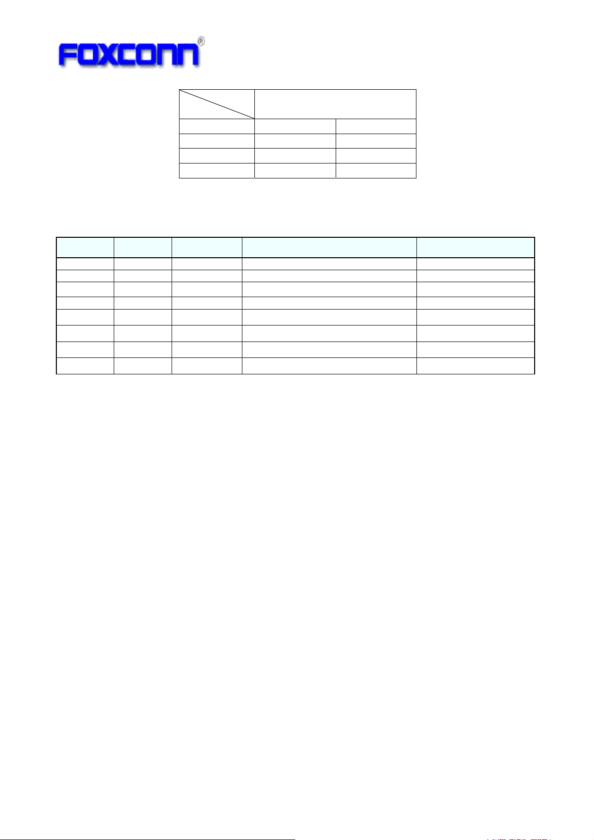
1.4 Module Weight
4
COMPANY CONFIDENTIAL
Model
Sample 1 2.6g 2.6g
Sample 2 2.6g 2.6g
Sample 3 2.6g 2.6g
J26H006.C01 J26H006.B01
Module Weight
1.5 Product Regulatory
Regulatory countries/IDs
Country Approval Certification Certification No. Remark
USA NO FCC TBD
Canada NO IC TBD
EU NO CE
Japan NO TELEC
….
TBD
TBD
2. Mechanical Specification
2.1 Module Mechanical Drawing
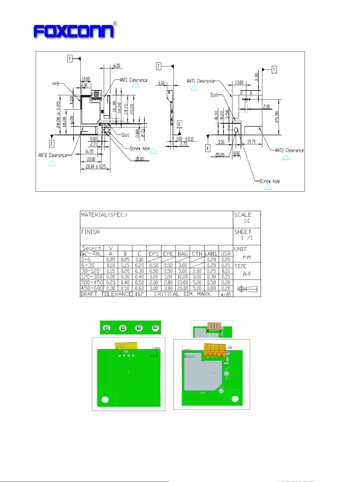
Ⅰ.For J26H006.C01: Typical module dimension (W x L) is 28mmx28mm.
5
COMPANY CONFIDENTIAL
Unit: mm
The tolerance for each mechanical dimension
1
Note
: The max shift degree of WTB connector is 2.3degree.
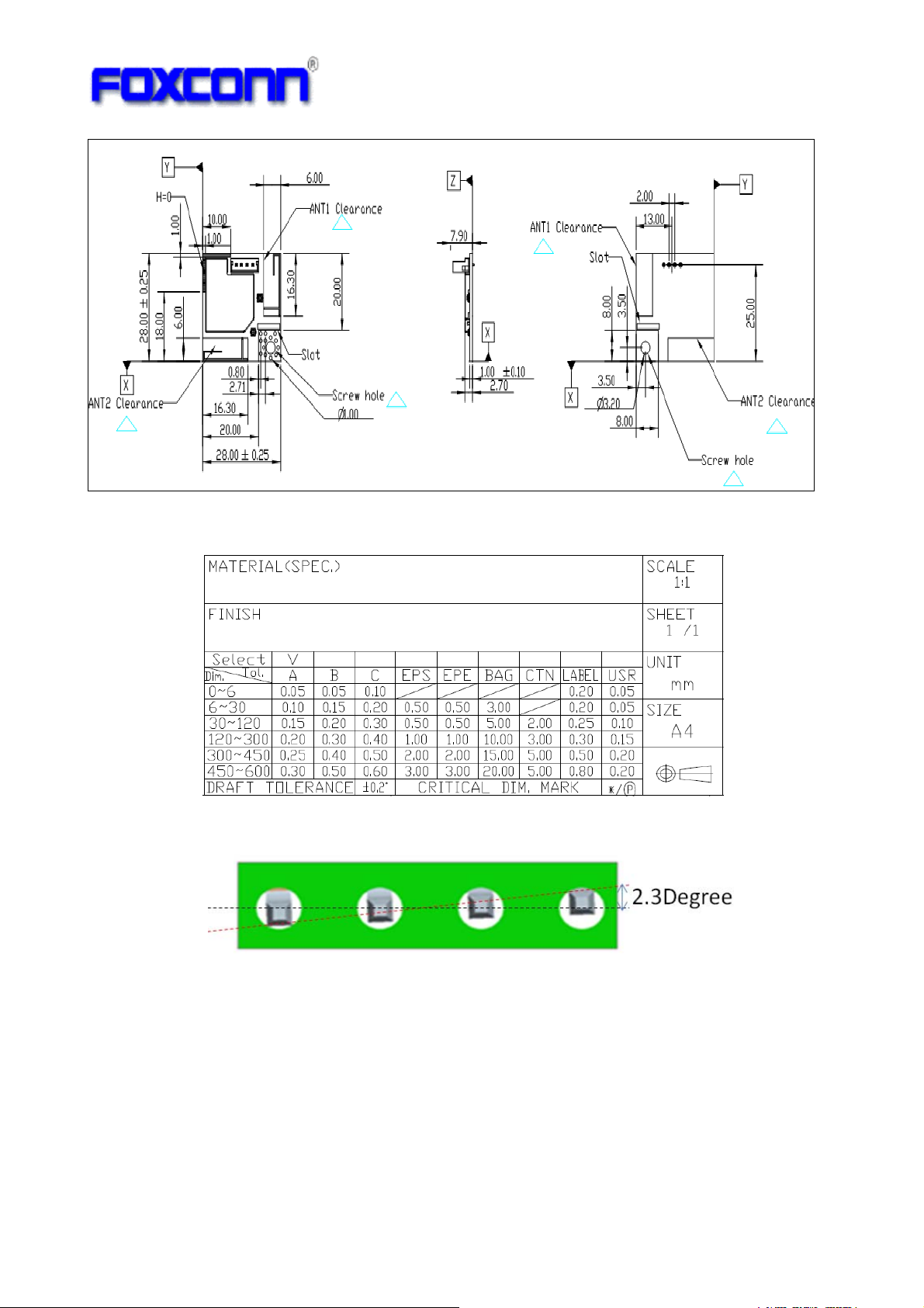
Ⅱ. For J26H006.B01: Typical module dimension (W x L) is 28mmx28mm.
6
COMPANY CONFIDENTIAL
The tolerance for each mechanical dimension
Unit: mm
2
Note
: The max shift degree of BTB connector is 2.3degree.
2.2 USB Connector
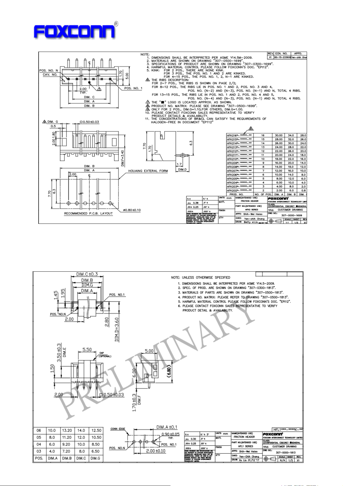
Ⅰ.For J26H006.C01:WTB Connector
¾ 4pin, 2.0mm pitch, Right angle type
¾ Part number: HFK2040-G1C3K-8F
¾ Vendor: Foxconn FIT
¾ High temperature plastic PA9T which meet SMT reflow profile(PIP)
7
COMPANY CONFIDENTIAL
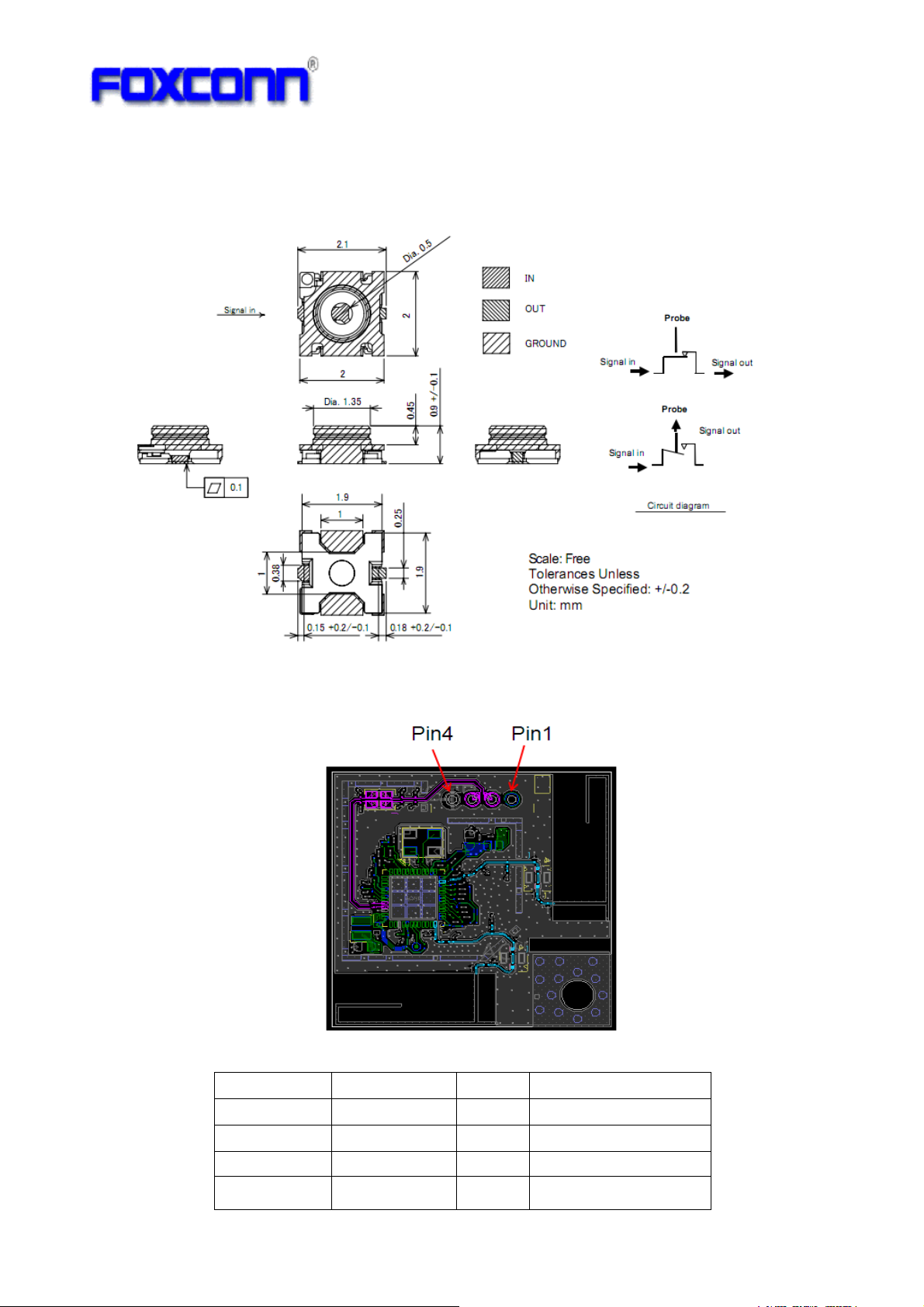
Ⅱ. For J26H006.B01: BTB Connector
¾ 4pin, 2.0mm pitch, Vertical type
¾ Part number: HFL1040-G1C3K-9F
¾ Vendor: Foxconn FIT
¾ High temperature plastic PA9T which meet SMT reflow profile(PIP)
8
COMPANY CONFIDENTIAL
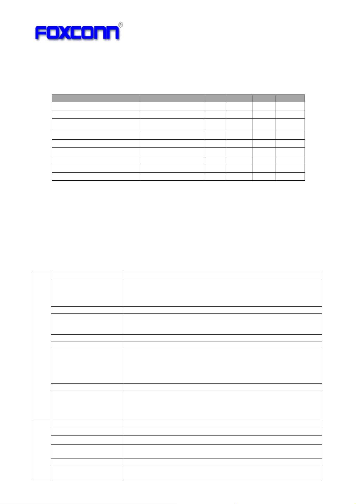
2.3 RF Switch Connector
¾ Part number: MM8030-2610RJ3
¾ Vendor: Murata
3.USB Connector Pin-out
Pin Number Pin Name I/O Description
1 VDD33 I DC 3.3V source input
2 USB_DN I/O USB D- Signal
3 USB_DP I/O USB D+ Signal
4 GND -- Ground
9
COMPANY CONFIDENTIAL
5. Electrical Specification
5.1 Recommended Operating Condition
Symbol Condition Min. Typ. Max Unit
3.3v(VDD33) Respect to GND 3.0 3.3 3.6 V
Max Ripple on Supplied Voltage 3.3V @full loading 95 330 mVpp
DC current @3.3V at full loading
(WiFi @TX and BT @ TX)
USB Suspend current -- 3.6 6 mA
Operating Temperature 0 +25 +70
Storage Temperature -25 25 +85
Operating Humidity 30~50% 90% RH
ESD HBM(contact) Standard:MIL-STD-883H +/-1.5 KV
ESD (indirect) Standard:EN61000-4-2 +/-4 KV
Function operation is not guaranteed outside of this limit, and operation outside of this limit for extended
period can adversely affect long-term reliability of the device.
- 257 500 mA
℃
℃
5.2 RF Characteristics
All typical performance specification are measured at RF connector port operating in +25℃@3.3V
3
: The target power table is just defined for board level.
Note
4
: Power is compliance with EVM IEEE spec based-on the parameter “disable full packet”
Note
Standard IEEE802.11b/g/n
Data Rate
Bandwidth 20MHz for 2.4GHz,
Modulation Techniques
Operating Frequency 2.412GHz~2.462GHz,
Media Access Control CSMA/CA with ACK
WiFi
Transmit Output Power
Frequency error +/-10ppm
Receiver Sensitivity
Radio Modulation FHSS
Operating Frequency 2.402GHz ~ 2.480GHz
Channel Numbers 79 channels with 1MHz BW
BDR Transmitter Output
Power
BDR Power Control 2dB≤Power Control Step≤8dB
BDR Initial Carrier Freq.
Tolerance
802.11b: 11, 5.5, 2, 1 Mbps;
802.11g: 54, 48, 36, 24, 18, 12, 9, 6 Mbps
802.11n:
HT20 mode: MCS0~MCS7,up to 72.2Mbp
802.11b: CCK, DQPSK, DBPSK
802.11g: 64QAM,16QAM, QPSK, BPSK
802.11n: 64QAM,16QAM, QPSK, BPSK
11b CCK_11Mbps:
11g 54Mbps: 25d
11n HT20_MCS7: 25dBm+/-1.5dB
11b 11Mbps: -83dBm@PER<=8%
11g 54Mbps: -70dBm@PER<=10%
11n HT20 MCS7: -67dBm@PER<=10%
0~+14dBm
≤ ± 75 kHz
23dBm+/-1.5dB
Bm+/-1.5dB
10
COMPANY CONFIDENTIAL
BDR Carrier Frequency
Drift
BDR Modulation
Characteristics
BDR Maximum Receiver
Signal
BDR Sensitivity -85dBm @ BER <= 0.1% at 1Mbps
BT
EDR Relative Power P[GFSK]-4dB<P[DPSK]< P[GFSK]+1dB
EDR Stability and Mod
Accuracy
BDR Frequency Range FL>2.4GHz,FH<2.4835GHz
EDR Sensitivity -80dBm@BER <= 0.01% at 2Mbps
BDR TX Output Spectrum
-20dB Bandwidth
LE Output Power 0~+14dBm
LE Modulation
Characteristics
LE Carrier frequency
offset and drift
LE Receiver Sensitivity -90dBm@PER <= 30.8%,GFSK,1Mbps
Drift Rate/50us <±20kHz
DH1: +/- 25kHz,DH3: +/- 40kHz,DH5: +/- 40kHz
140kHz ≤ ∆f1avg ≤175kHz
∆f2max ≥115kHz
∆f2avg/∆f1avg ≥0.8
-20dBm@ BER <= 0.1% at 1Mbps
-75 kHz <ωi < 75 kHz
-10kHz<ω0 <10kHz
RMS DEVM<=0.13 for all 8DPSK @3Mbps
Peak DEVM<=0.25 for all 8DPSK @3Mbps
99% DEVM<=0.2 for 99% 8DPSK @3Mbps
-80dBm@BER <= 0.01% at 3Mbps
≤1MHz
225kHz ≤ ∆f1avg ≤275kHz;
∆f2max ≥185kHz for at least 99.9% test packets;
∆f2avg/∆f1avg ≥0.8
Carrier frequency offset: ±150kHz
Carrier Drift: ≤50kHz
Drift rate: ≤20kHz/50us
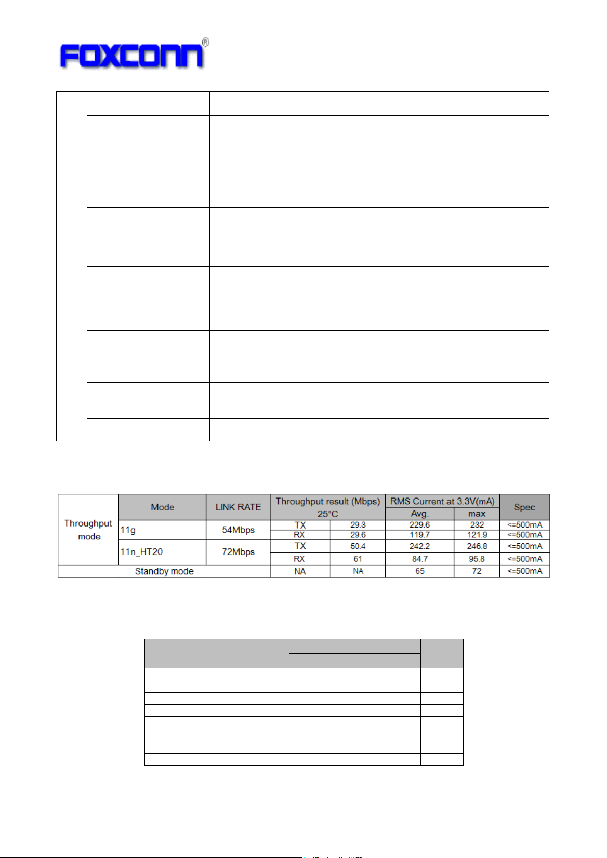
5.3 Current consumption
5.3.1 WiFi current consumption
Remark: Base-on Win7 OS to do WiFi only throughput tests. The Standby mode means “module connect to
AP only, and don’t transfer the data.”
5.3.2 Bluetooth current consumption
Test Condition
Idle mode( power on only) 63.7 mA
BT BDR 1DH5 TX@6dBm 115 mA
BT BDR 1DH5 Rx 87 mA
BT EDR 2DH5 TX@6dBm 116 mA
BT EDR 2DH5 Rx 87 mA
BLE TX@6dBm 78 mA
BLE Rx 87 mA
Standby mode* 69 mA
Avg. Current at 3.3V
Min Typ. Max
Unit
Remark: The result is base-on Win7 driver.
The Idle mode means “ module power on only, don’t open any testing tool”
The standby mode means “module connect to BT device only, and don’t transfer the data”
11
COMPANY CONFIDENTIAL
C
5.4 eFuse Content
5.4.1 WiFi eFuse
Revision Note
EEPROM Version Chang Lists Owner Date Remark
address Value for WiFi Efuse address 0xC4, change
0xC4 0x01
value from 0x00 to 0x01
address 0 1 2 3 4 5 6 7 8 9 A B C D E F Path A cck TX calibration power index
eFuse for WiFi eFuse address
0 29 81007C01880700 A004 EC3512C0A2D8
1 16 1413121212191817 161602FFFFFFFF Path A 11n HT40 mcs7 TX calibratio n
2 FF FFFFFF FFFFFFFFFF FFFFFFFFFFFFFF
3 FF FFFFFFFFFFFFFFFF FF141414131212 0x1B Path A pow er diff in dex (offse t) fixed value
4 17 1717161502FFFFFF FF FFFFFFFFFFFF
5 FF FF FF FF FF FF FF FF FF FF FF FF FF FF FF FF Path B cck TX power calibration index
6 FF FFFFFF FFFFFFFFFF FFFFFFFFFFFFFF
7 FF FF FF FF FF FF FF FF FF FF FF FF FF FF FF FF Path B 11n HT40 mcs7 TX calibration power index
8 FF FFFFFF FFFFFFFFFF FFFFFFFFFFFFFF
9 FF FFFFFF FFFFFFFFFF FFFFFFFFFFFFFF 0x45 Path B power diff index(offset) fixed value
A FF FFFFFFFFFFFFFFFF FF FFFFFFFFFFFF
B FFFFFFFFFFFFFFFF20 1F1A000000FFFF 0xB8 channel plan:0x20 fixed value
C FF292050010000FF00 FF11FFFFFFFFFF
D FF FFFFFFFFFFFFFFFF FF FFFFFFFFFFFF 0xB9 Crystal calibration data
E FFFFFFFFFFFFFFFFFF FF FFFFFFFFFFFF
F FFFFFFFFFFFFFFFFFF FF FFFFFFFFFFFF 0xBA Thermal meter
10 DA 0B 23 D7 E7 46 07 D8 0F 99 16 57 F3 09 03 52
11 65 61 6C 74 65 6B 16 03 38 30 32 2E 31 31 6E 20 0xC3 Antann a settin g fixed value
12 57 4 C 41 4E 20 4 1 64 61 70 74 65 72 00 FF FF FF
13 FF FF FF FF FF FF FF FF FF FF FF FF FF FF FF FF 0xC4 EEPROM version: 0x01 fixed value
14 FF FF FF FF FF FF FF 0F FF F F FF FF FF FF FF FF
15 FF FF FF FF FF FF FF FF FF FF FF FF FF FF FF FF 0x100~0x101 VID:0x0BDA fixed value
16 FF FF FF FF FF FF FF FF FF FF FF FF FF FF FF FF
17 FF FF FF FF FF FF FF FF FF FF FF FF FF FF FF FF 0x102~0x103 PID:0xD723 fixed value
18 FF FF FF FF FF FF FF FF 6 B 41 22 D D 53 59 86 D1
19 70 8F 00 00 10 16 40 00 FC 8C 00 11 9B 00 00 0A 0x107~0x10
1A FF FF FF FF FF FF FF FF FF FF FF FF FF FF FF FF
1B FF FF FF FF FF FF FF FF FF FF FF FF FF FF FF FF 0x00~0x0F
1C FF FF FF FF FF FF FF FF FF FF FF FF FF FF FF FF 0xBB~0xBD
1D FF FF FF FF FF FF FF FF FF FF FF FF FF FF FF FF 0xC1~0xC2
1E FF FF FF FF FF FF FF FF FF FF FF FF FF FF FF FF 0xC4~0xC6
1F FF FF FF FF FF FF FF FF FF FF FF FF FF FF FF FF 0xC8~0xCa
Note:
USB Vendor ID (VID): 0x0BDA
USB Product ID (PID): 0xD723
Fly. Huang 2017/08/11 PVT
WiFi MAC: D80F991657F3 consistency
other config fixed vuale
0x104~0x12C
0x147
0x188~0x19F
12
 Loading...