

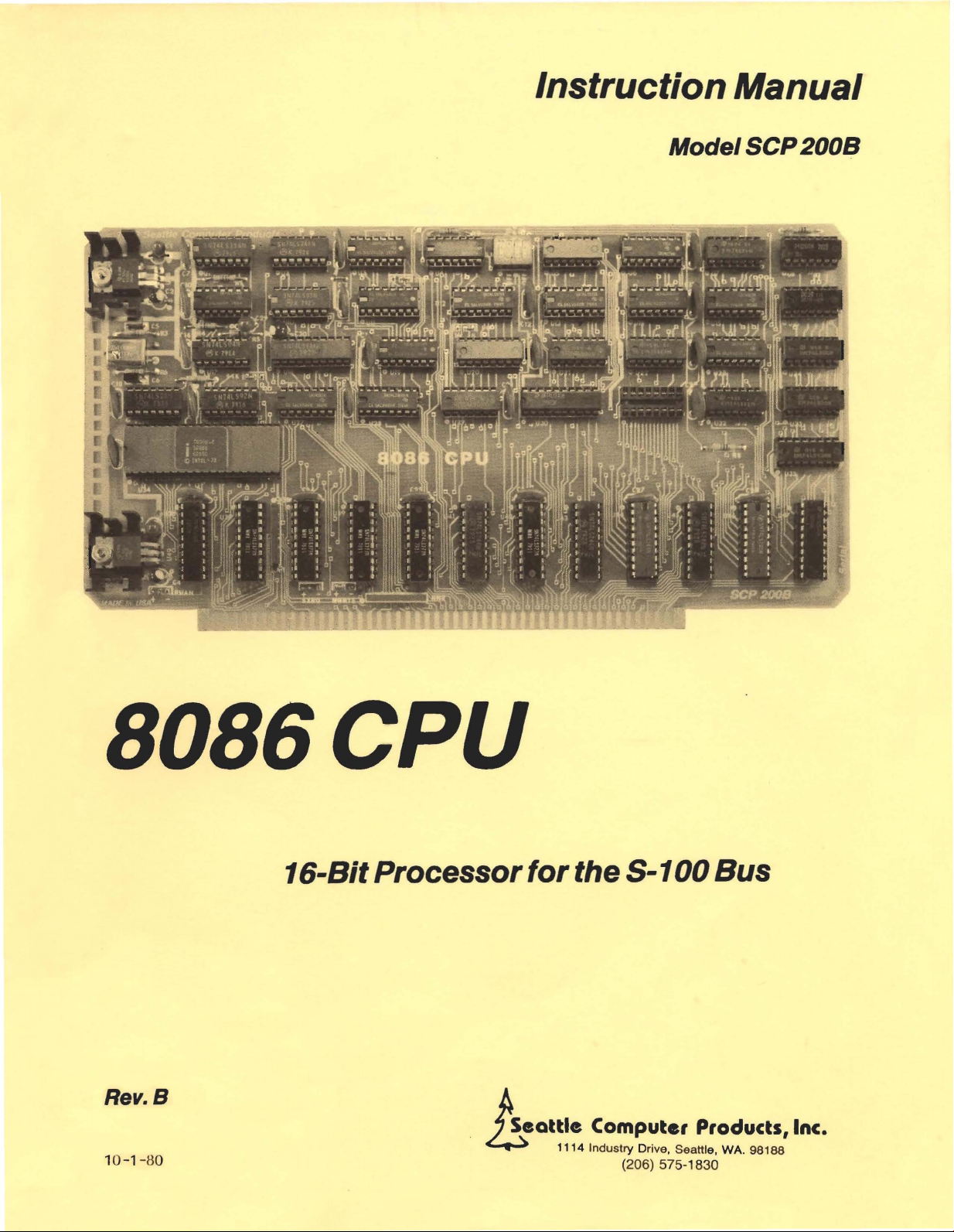
Instruction Manual
Model
SCP
2008
BOB6CPU
16-BitProcessorforthe
Rev.S
.
Asaattla
10-1-80
~
5-100
(omputar
1114 Industry Drive. Seattle.
(206) 575-1830
Products,Inc.
Bus
WA.
98188
TABLE
OF
CONTENTS
Features
Configuration
Technical
1.
0
General
2.0
Features
3.0
S-100
4.0
A.C.
Theory
One-Year
of
Limited
Options.
Description.
and
Connector
Characteristics.
Operation.
Warranty.
Comparisons
Layout.
to
IEEE
Standard.
..
3
3
5
5
5
9
.10
.14
.21
- 2 -

Features
> Advanced
hardware
16-bit
multiply and
architecture
divide,
and high-speed
> Fully meets IEEE-696 standard
throughput.
>
Completely
>
Directly
>Has a minimum
with
static
>Entire design
>Configurable
jumpers.
compatible
addresses upto1 megabyteofmemory,
instruction
memoryof250 nsec.orfaster.
conforms
to
with
8-bit
execution
to
IEEE-696 standard
meet a wide range
Configuration Options
SWITCH
SELECTED
OPTIONS
of
the
for
memory
of
8086 includes a versatile range
string
operations.
16-bit
time
operation
and
I/O
eliminating
of
only
for
the
system requirements
on
devices
250 nanoseconds,
5-100
bus.
the
with
reduced
the need
through
5-100
of
addressing modes,
bus,
allowing
performance.
for
"bank select".
yet
needs
its numerous switches and
no
maximum
"wait
states"
5-1,
located
of
segments
Segment 1:
Segment 2: Sixteen aCknowledge--the closed
line
to
forces
eight-bit
capability
eight-bit
Segment3:This
closed
defeated by a jumper and
own
wait
by
the
8MHz, 250nS
states are required and the
the
determineifthe
the
CPU
systems used this line (60)
as
or
sixteen-bit
position
Segment 4: Closing this
state
peripheral.
or
near the
switch
Not
used
to
do
well.
It allows
switch
selects 4MHz, open selects 8MHz. On 4MHz CPU cards this
generator,
With
the
faster chips must be used. Thus,
topofthe
and
their
function
on
this
board.
peripheral
all
eight
memories.
hasnoeffect;
closing
4MHz
switch
being accessed can
bit
transfers. The
him
to
selects between4MHz
switch
segment 4 adds one
clock,
segment should remain in the "open"oroff
board
are:
for
another
compare
the
CPU
adds
one
memory
between U4 and U5 has
position
do
switchisprovided
purpose.
program
and8MHz
always runsat4MHz.
wait
state
wait
chip speed requirements
with
allows the
a sixteen
The
execution
operation
to
each
stateinadditiontothe one(s) requested
most
memory,
- 3 -
three
active
CPUtolookatthe
bit
transfer.
because
switch
bus
allows the user
time
differences
with
8MHz
cycle.
and a 4MHz
If a
are
in excessof450n5.
position.
segments. The
The open
some
of
while
CPU
switch
peripheral
clock,
sXTN*
position
the
early
another
using
cards.
segment is
no
has
The
it's
At
wait
JUMPERS
There are six jumpers on the
chart
below
shows
NAME
STV (Status
STK
their
Valid)
"normar
positions.
1-0
PHANTOM*
SXI<Q
(sXTRQ*)
MWRITE
Each
of
these jumpers
should change themtothe alternate
will
boardtoallow
NO~MAL
POSITION
"0"
"E"
"8"
"+"
"+"
"+"
be discussed in
position.
configuring
more
detail
your
CPU
for
special
~EMA~KS
Used
with
OMA
Used
with
DMA
Puts
lower
8-bit
address on
Connects
Connects Sixteen Request line
Connects
to
enable
upper
PHANTOM* line
MWRITE
you
to
determineifyou
situations.
1-0
8-bits
line
The
STV (Status
during
is
OMA:Inthe
three-stated
Valid)--this jumper
"E"
position
when
COSH*
(control
the CPU always drives the pSTVAL* line.Inthe
it.
STK--this jumper
"E"
position
indicate
5-100
information
jumper should
lower
I/O
locations
cards
may
located
addresses. The PHANTOM* signal
memory
the
PHANTOM* jumper in the "_"
pin
and middle address bytes are the same.
addressing.
PHANTOM*
whichdonot
be
PHANTOM* generated
the CPU always drives this line
4MHzoperation.Inthe
18)
is
low
1-0
--
In
onto
the
be
in the
--
located
composedofup
in the
locatedatthe higher addresses. If
above
lowest
controls
"D"
allowing
the
next
This
have extended addressing. Through the
the
normal
higher
16-bit
CPU
board
the
lowest
to
64K
64K and
on
the CPU
position.
UMA
"8"
position.
controls
disable, S-100
the
functionofthe
position,
devicetodrive
position,
8 address bits. If
Most
generates a PHANTOM* signal wheneveritaddresses
64K. This signal may be used
of
the
older,
newer,
extended addressable
would
prevent
board
the
function
pin
19)islow
"SPEED"
with
a high
this lineisthree-stated
it.
this jumper copies the
your
existing
The
upper address byte,
non-extended
the
older
your
system
should be disconnected
of
line (S-100 pin
to
indicate
1-0
I-Q
devices use addressing in
useofthis PHANTOM· signal, a system
addressable
memory
uses
this signal
the pSTVAL* line (S-100
"Ui
allowing
devices
to
memory,
the OMA
98)
during OMA.Inthe
8MHz
when
lower
disable
from
operation
SDSl:3·
8 bits
usea16-bit
A16-A23,isnever used in
older,
memory
located
from
interfering
for
some
the
bus
pin
position
devicetodrive
(status disable,
of
8-bit
which
in the higher
other
by
this line
or
low
I-Q
address
address, the
which
memory
memory
would
with
purpose,
putting
25)
'-
to
the
be
the
the
sXT~Q*
16-bit
postion.Ifyoudonot
the jumper
sXT~Q*
position.
transfer.
line should be
could
--
The Sixteen Request signalisgenerated by the
In
our
be
system, using
have
16-bit
in
either
disconnected
position.Ifyour
16-bit
memoryinyour
between the
memory,
system
- 4 -
this jumper should be
system, the signal
uses
bus
CPU
and the
CPU
wheneveritwants
connected
would
line 58
bus
for
by placing the jumper in the "_"
serve
some
no
other
purpose and
purpose, the
to
in the
do
a
"+"
•
MWRITE--This jumper connects the
connected
is
generated somewhere else in the system, such
Disconnect by placing the jumper in the
and used by
most
systemsasthe
MWRITE
"_"
Technical
1.0 General
CPU
The SCP-2oo
to
interfaceitto
upgrade the
foundationofa high
Some
document.Athorough
bus.
The asterisk
2.0
Features and ComparisonstoProposed Standard
2.1
Clock
All
timing
8086 chip itself
operation
All 4
(formerly
approximately
to
be disabled
250
more
addition, the line
MHz,
only,
MHz-only
On the bus, CLOCK (pin 49) is always 2 MHz,
~2,
The 8086 allows 3
ns
memoryisrequired
time
is required, the
low
for4MHz.
the 5-100
performance
prior
knowledgeofthe fundamentalsofthe S-1oo
signals are
is
while
CPU cards are
pin 24) are equal
square waves. pSTVAL* and!>are equal in phase,
(tristate)
cardisan
businaccordance
of
performance
understanding requires
(*)
denotesanactive-low
either4or
the
higher-priced
by CDSB* (pin
clock
whileat4 MHz,
card
formerly
This may be usedtocontrol
named sSTACK (pin 98)isdriven
Intel 8086
present S-1oo systems by swapping
16-bit
derived
8 MHz. A
factory
to
cycles
may
computer.
from
lower-priced
version
upgradableto4/8
the
clock
19)
while~is
for
memory
be
switched
lineofthe
primary
position.
write
line. It should be disconnectedifMWRITE
as
on a
DescrlpUon
CPU
chip
with
with
the
proposed
familiarity
signal.
an
on-board
frequency
over
has
access (minus delays and setup
500nsaccess
wait
with
24 MHz
version
switch
MHz.
while
of
never disabled.
to
insertawait
state
CPU
board
control
the
electrical
IEEE
bus
is essentialtounderstanding this
the
IEEE-696 standard
oscillator.
of
selectionofeither
pSTVAL*
the
CPU(4or
but
timeisallowed.
with
generatorsofperipherals.
to
the bus. Itisnormally
panel
CPU
the
(formerly
pSTVAL* may be
state in
clock
or
the
and mechanical hardware
standard. It may be used
cards
boardiscapable
oritmay
The
clock
a 4
m1,
8 MHz). All three are
(see
every
speed
status--high
motherboard.
to
form
the
for
the S-100
rate
of
the
of
4 MHz
or
8 MHz
pin
time).At8 MHz,
section
bus
clock.
25)
and
configured
4.)
cycle•
for
~
If
.,
8
2.2 Data
logic in
beginning
2.2.1 sXTKQ*, SIXTN*
The
parallel
ns
requested (externallyoron-board),
SIXTN*islatched on the rising edge
wait
8-bit
bus
16-bit
Bus
The 8086
eitheroftwo
If
the
addressed device may then respond by pulling
transfer.
before
state, and changes
If, at the
mode
Should
pins
58or60,
modeisnot
CPU
chip
modes:
of
each
bus
cycle, depending on
processor
Timing
the rising edge
time
is selected.
the
8086 CPU .card be used in a system
either
possible.
is a
16-bit
wishes
for
SIXTN* is the sameasthe READY lines
of
after
this
SIXTN*islatched,itis
Utherwise,
or
bothofthese lines may
processor
8-bit
modeor16-bit
to
readorwrite
~
that
ends pSYNC. An
SlXTN* may be delayed until
of
time
are
sXTRO* is kept
CPU
~,
either
irrelevant.
whichisinterfacedtothe S-100 bus by the
mode.
status and
16 bits, sXTRO* (pin 58) on the
low
near the endofpSYNCornear the endofthe last
high
(inactive),
low
which
be
The
modeisselected dynamicallyatthe
bus
response,asfollows:
SIXTN* (pin 60)ifit
(RDY/XRDY)--it
exception
and
16-bit
previously
disconnected
to
thisisthatifa
near
the endofthe last
then sXTRO*isremoved
mode is selected.
from
can
defined a
CPU
busisdriven
performa16-bit
must be valid 50
wait
wait
and
conflicting
logic.Inthis case,
- 5 -
support
low.
state
state.
double
use
for
is

2.2.2
8-Bit
Mode
2.2.2.1
Logic
location);
processor's
data lines
2.2.2.2
Simple
on
the
2)
to
8-Bit
card
from
low
8 data lines
the
00
Double 8-l:Jit Mode. This
even address but the
put
intoawait
back
-to-back,
simple
8-bit
the second
2.2.3
16-l:Jit Mode
In
data
to/from
to/from
2.2.4 Data
I:Jringing
2.2.5 Co
this mode, 16 bitsofdata are
the odd addressed
Driver
mpatibility
state
firstatthe even address, thenatthe
mode
cycleiscomplete.
the even addressed
Disable
low
Mode. This
routes
modeisused when the
data1)from
the01bus
to
the01bustothe processor's high 8
to
the
DO
bus
bus
(write
memory
for
at
odd
location).
mode
or
I/O
least 4
(write
is used when the
deviceisnot
clock
even
capable
periods
odd.
above,
OOOSB* (pin
except
location
the data resulting
transferred
location
(processor's
(processor's high 8
23)
will
disable
from
in parallel in one
both
the data
processor
the processor's
data
lines (read
location);
processor
while
Each
the
low
8 data lines), and
data
wishestotransferaword
of
16-bit
on-board
bus
cycleisessentially the sameasin
firstoftwo
lines).
input
wishes
4)
to
transfer
low
8 data lines (read even
odd
location);
from
the processor's high 8
operation.
logic
runs
The
two
read cycles is latched until
bus
cycle.
The DO lines
the01lines
and data
output
drivers.
only1byte.
3)
from
the
on
an
processor
bus
cycles
carry
carry
data
is
The techniques
proposed
memory
environment
2.2.6
CPU
Further,
arbitrary
2.3
Address
2.3.1
All 24 are
address,
IEEE
standard. They allow the CPU
(for
easy upgrade),
(e.g.,
16-bit
Oata Line
Connector
chip.
by using
Connector
]1, a
Pins1to
DOD5~*
16-pinICsocket,isprovided
16ofthis
instructionsordata may be fedto8086
!:Jus
Memory
The
Address
proposed
driven
A20-A23
IEEE
by the CPU
are always
2.3.1.1 Phantom
Traditionally,
their
address space
not
possible because these cards
However,
memory
may
lowest
OMA
using
special
location
be
used
to
64K, when PHANTOM* is
The
PHANTOM*-driving
controllers
onlya16-bit
5-100
to
provision
ABOVE
disable
which
address.
for
mode
memoriesintime-critical
to
selection and
with
new
16-bit
socket
are
disable the data
16-bit
to
run
memory
code
connected
drivers
through
standard dedicates 24 pins on the
card;
driven
memory
64K bytes.
has
been made on
the
lowest
memories
not
circutiry
usea24-bit
however
low.
cards have decoded
Ordinarily,
will
appear in the same
64K is addressed, PHANTOM* (pin 67)isdriven
witha16-bit
being
address need
since
useofsuch cards in a system
the
8086 CPU card, selected by a jumper: Whenever a
address.
driven.
on the
CPU
notbeconcerned
- 6 -
transfer
without
(for
are in
modification
high
performance),
areas).
to
allow
monitoring
to
ADOtoAD15ofthe
when the
this
connector.
bus
for
the
8086 chip
only
the
relative
Thus
these memories appear only in the
card
continuestofunction
board
memory
itself
lowest
position
with
strict
accordance
with
or
evenina mixed
with
ordinary
8-bit
the data linesofthe 8086
8086, respectively.
is
reading (pOBIN
address
generates
only
16 address lines,
with
more
in each 64K
active),
information.
20
bits
limiting
than
64K
block.
low,
which
during DMA. Thus
the presenceofmemories
the
of
is

2.3.2
"put/Output
Address
However,
/".
unfortunately
lines. To maintain
away
2.3.3 Address
2.4 Status
proposed
The
traditionally
many devices have been designed
the
high 8 bitsofthe 8086's
Driver
Bus
CPU
low
card
Bringing
The
NAME
sMEMR
sM1
slNP 46
sOUT
sWO*
slNTA
sHLTA
sXTRQ*
the
compatibility
Disable
ADSB* (pin
drives all status lines in
PIN
47
44
45
97
96
48
58
standard allows and the 8086
lower
8 bits and
with
I/O
22)
will
upper
such devices the
address and substitute
disable the address
accordance
8 bits
which
CPU
chip
supports a
of
the address have been the same, and
decode
with
support
the
drivers.
the
their
I/O
logic
low8bits.
proposed
address
can be jumpered
16-bit
from
standard. They are:
I/O
address.
the upper 8
to
throw
2.4.1 Status
optionally
the
sST
Control
2.5
Traditionally,
goes
highaspSYNC goes
Driver
Hringing
be
ACK status line.
Bus
All
control
OUTPUTS
pSYNC
pSTVAL-
pDBIN
pWI<pH
lOA
Disable
low
SDSH*
disabled by this signalifnecessary,
lines are in
another
PIN
76
25
78
77
26
control
lowifthe
(pin 18)
accordance
INPUTS
ROY
IN
NMIHalOSIXTN-
line
has
will
disable the status
with
the
XROY
I-
been
pWAIT
busisput
intoawait
to
be consistent
proposed
PIN
72
3
73
12
74
60
(pin
27).
state.
drivers.
standard. They are:
This line is
Clock
with
speed status, pin 98, may
its
driven
traditional
by the
definition
CPU
card
as
and
2.5.1
r-
pSTVAL-,has
be disabled.
Control
Bringing
Driver
not
Disable
low
CUSH- (pin 19)
been disabled by this signal. A jumperisprovidedtoselect whetherornotitwill
will
disable the
control
drivers.
Traditionally,
pin 25,
- 7 -
now
2.6
Power
Only
regulators
2.7
Other
2.7.1 Reset
Supply
+8V (pins 1 &
provide+5Vat
lines
51)
1.2 A
and GROUND (pins 50 &
(typical)toall
circuitry.
100)
are used
for
power.
Two
on-card
POC* (pin 99)
the
card.
During this
resetatany
After
fo
Manual
2.7.2
system, this
2.8
modification,
data.
to
the
may be used
the
into
pins 9
When
the
circuit
(this
44 (the
from
r details.
MWKITE
The
CPU
Front
Panel
Thereiscurrently
Note
8086's Address/Data linesisprovided,
IMSAI
front
pins 1to8ofthe
to
16
the
processor
word
will
The
modification
board,
trace
comesinat45degrees). Install a jumper
next
both
traces.
isatotem-pole
time
timebydriving
reset,
the
card
normally
function
an
that
with
of
maybedefeated by
Co
mpatibility
IMSAI
EXAMINE
an
IMSAI
panel
connector
the cable plug
does a ·double
RESET*
8086
no
front
and
socket
RESET·
will
generates
hardware
panel may be used
DEPOSIT
front
output
(pin 75),
low
begin
lJaneltoobserve 8 data bitsata
are used. To observe the
(the cable should extend
into
pins 16to9
gulp·--two
driven
normally
for5or
program
MWKITE
removing
front
panel
functions
low
an
morepcycles.
executionatOFFFFOH.
(pin
68).Ifthis
a jumper.
for
to
run, stop, single step, and observe address and
will
not
with
pins
of
the
8-bit
reads when 16 bits are
be displayed sequentially on the high data lines.
to
the
IMSAI
front
paneltoallow
near the edge
trace
to
the
This change
connector
right).Itwill
will
not
below
address
be necessary
affect
operationofthe
from
to
momentarily
input,isalso
the 8086onthe S-100 bus. With one simple
work.A16-pin
1-16
wiredtoADO-AD15, respectively. This
low
downward).
socket
single steppingismade on the
switch6.Cut
this
scrape away a
front
when
powerisfirst
driven
See
signal is generated elsewhereinthe
time.
(even) data byte, plug pins 16to9
For
(the cable should extend
the tracetoconnector
trace
to
panel
low.
The
Intel's 8086 Family User's
socket
Only pins 9
the high
the
portion
with
directly
(odd)
needed--both
trace
connectedtopin
of
the solder mask
8080 CPUs.
applied
CPU may be
connected
through
front
16
data byte,
upward).
halves
of
pi n 39
the
to
of
of
- 8 -
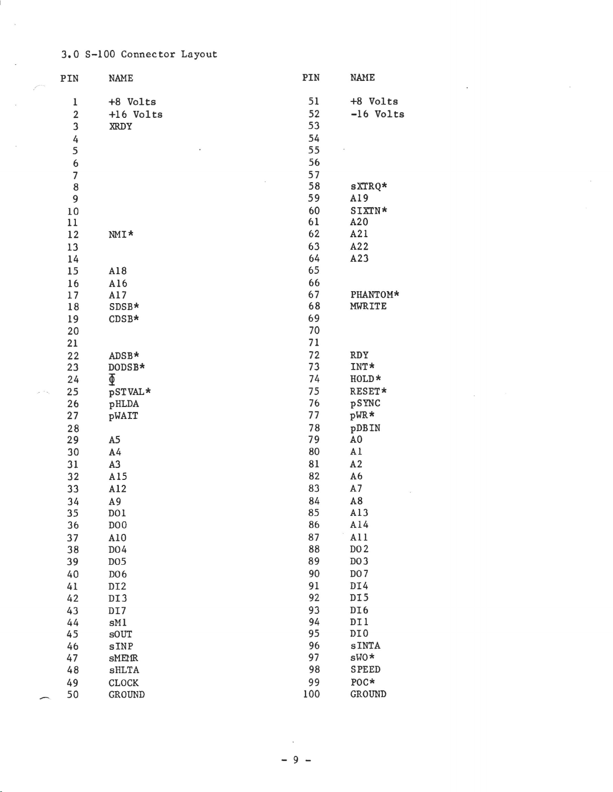
3.0
S-100
Connector
Layout
/ ...•
PIN
10
11
12
13
14
15
16
17
18
19
20
21
22
23
24
25
26
27
28
29
30
31
32
33
34
35
36
37
38
39
40
41
42
43
44
45
46
47
48
49
50
NAME
+8
+16
XRDY
Volts
Volts
1
2
3
4
5
6
7
8
9
PIN
51
52
53
54
55
56
57
58
59
60
61
NMI*
62
63
64
A18
A16
A17
SDSB*
CDSB*
65
66
67
68
69
NAHE
+8
Volts
-16
Volts
sXIRQ*
A19
SIXIN*
A20
A21
A22
A23
PHANTOM*
MWRITE
70
71
ADSB*
DODSB*
~
pSTVAL*
pHLDA
pWAIT
AS
A4
A3
A15
A12
A9
DOl
DOO
AIO
D04
D05
D06
DI2
DI3
DI7
sMl
sOUT
sINP
sMEHR
sHLTA
CLOCK
GROUND
72
73
74
75
76
77
78
79
80
81
82
83
84
85
86
87
88
89
90
91
92
93
94
95
96
97
98
99
100
RDY
INT*
HOLD
*
RESET*
pSYNC
pWR*
pDBIN
AO
Al
A2
A6
A7
A8
Al3
A14
All
D02
D03
D07
DI4
DI5
DI6
DI1
DIO
sINTA
sWO*
SPEED
POC*
GROUND
- 9 -

4.0
A.C.
Characteristics
The
symbol
in
the
left
column
is
TAYBZ
of
the
form
where
It
second
Signal
A C D I -
H -
o -
R -
S V -
W -
T means a
means
signal
Names
Address
Clock
pDBIN
Data-in
HWRITE
Data-out
Ready
Status
pSTVAL*
pWR*
Y - pSync
goes
High."
appropriate
clock,
the
for
proposed
standard
A,B
are
Y,Z
are
the
time
The
following
bus
(~)
(RDY
bus
For
example,
Times
for
an 8
S-100
is6MHz.
timing
abbreviations
abbreviations
from
reaches
/XRDY
/SIXfN*)
TRVCH
specified
a
worst-case
MHz
clock,
standard
measurement;
of
of
the
first
the
second
abbreviations
means "Time
are
in
nanoseconds,
specification.
and
for
at
411Hz. The maximum
signal
signal
signal
level.
are
from
comparison
names;
levels.
reaching
used:
H L -
X -
Ready becomes
either
Times
purposes,
the
Signal
High
Low
V -
Valid
Invalid
minimum
listed
clock
first
Levels
level
Valid
or
are
the
requirements
speed
until
until
maximum
for
a 4
covered
Clock
as
MHz
by
the
of
the
- 10 -
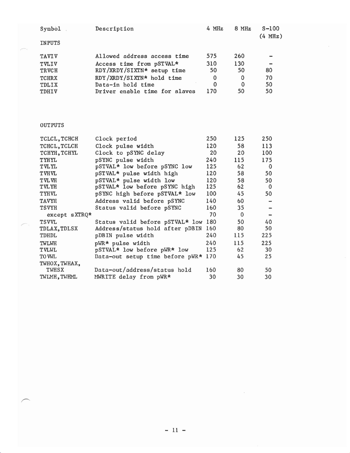
Symbol
INPUTS
Description
4
MHz
8
MHz
S-100
MHz)
(4
TAVIV
TVLIV
TRVCH
TCHRX
TDLIX
TDHIV
Allowed
Access
RDY
RDY
Data-in
Driver
address
time
/XRDY
from
/SIXI'N*
/XRDY/SIXI'N*
hold
time
enable
access
pSTVAL*
setup
hold
time
for
time
time
time
slaves
575
260
310 130
50 50
0
0 0
170
50
80
0
70
50
50
OUTPUTS
TCLCL,TCHCH
TCHCL,TCLCH
TCHYH,TCHYL
TYHYL
TVLYL
TVHVL
TVLVH
TVLYH
TYHVL
TAVYH
TSVYH
except
/~
......
TSVVL
sXI'RQ*
TDLAX,TDLSX
TDHDL
TWLWH
TVLWL
TOVWL
TWHOX,
TWHAX,
TWHSX
TWLMH,
TIIHML
Clock
Clock
Clock
pSYNC
pSTVAL*
pSTVAL*
pSTVAL*
pSTVAL*
pSYNC
Address
Status
Status
Address/status
pDBIN
pWR*
pSTVAL*
Data-out
period
pulse
to
pulse
pulse
pulse
low
high
valid
valid
valid
pulse
pulse
pSYNC
low
before
width
low
setup
width
delay
width
before
width
width
before
pSTVAL*
before
before
before
hold
width
before
time
Data-out/address/status
ffiY:RITE
delay
from
pWR*
pSYNC
low
high
low 120
pSYNC
high
low
pSYNC
pSYNC
pSTVAL*
after
pWR*
before
low 180
pDBIN
low
pWR*
hold
250 125
120 58
20
20
250
113
100
240 115 175
125
120 58
125
100
140
160
70
160
62
58
62
45
60
35
50
80
50
50
50
0
40
50
240 115 225
240
125
170
160
30 30
115
62
45
80
225
30
25
50
30
0
0
-
11
-

f--
~
j
STANDARD BUS
TCHCL-
f--TCLCH-
1\
TYHYL
CYCLE
pSYNC
pSTVAL*
ADDRESS
STATUS
pDBIN
TCHYH
I-TVLYH
1\
I-----TAVYH-
111
\/\
I--TSVYH-
X
r--
I
TSVVL
J
TYHVL
TVHVL-
TVLYL-
r-TVLVH-!
TCHYL
1\
-+--TDHIV-
TDHDL
I
~TDLAX-
TDLSX-
\
DATA
DATA
OUT
pWR*
MWRITE
IN
--f
TAVIV
1\
f---TOVWL
I----TVLWL-
TWLMH-
- 12 -
j----.
II
J
~~
~TDLlX
TWHOX
____
TWHML
X
TWLWH
,
1\
-
c-

pSYNC
RDY,XRDY
SIXTN*
BUS CYCLE WITH ONE
WAIT
STATE
pWAIT
pDBIN
pWR*
I
I
\
\
\
I
- 13 -

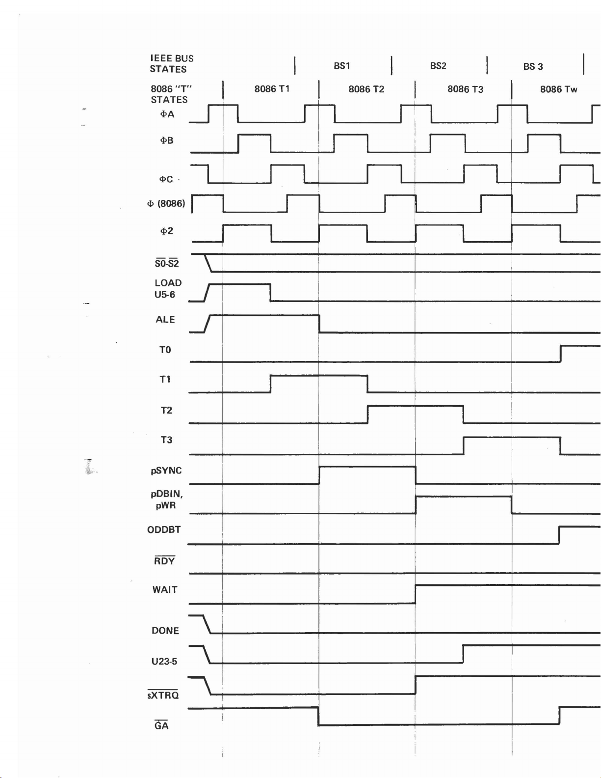
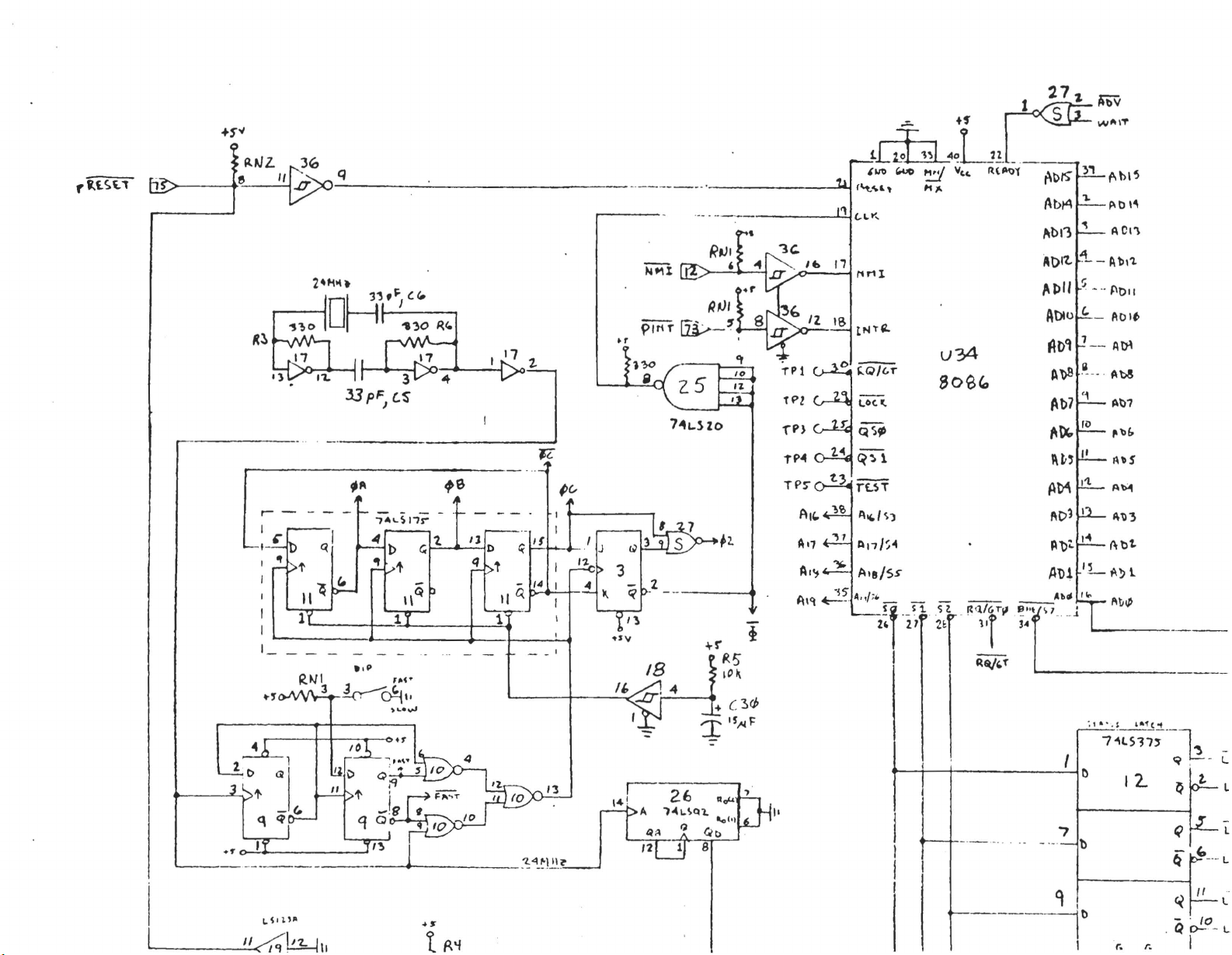
Theory
of
Operation
Mostofthe signals described
Operation.
various
names
Clock
The main
clock.
outputofthe SP4/8
The 24 MHz
The12or
24 MHz signal
~U,
and
section
to
gate
timing
~us
Cycle
The
8086
or
moreofthe
from
U4,anAND
U5.
As
next
falling edge
register.
Latch Enable) is generated by half
low
on
m2.
ALE
multiplexed address/data pins the address
last
through
The
diagram
signals
on
Circuitry
The 24 MHz
~c.
of
form
relationships between these
itselfisoperated
shown in the diagram,
LOADisalso used
the
followed
the
schematic.
timing
24 MHz
Control
is used
source
clockisalso
output
by
three
<PC
is shifted
U25 and fed
~2,
which
Circuitry
three
gate
of
next
falling edge
to
the
bus
clockisdivided
switch.
status lines
from
~2.
latch the address
cycle.
below
shows a
by
an
For
example, ALE*isthe same
for
the 8086
are shown in the
typical
asterisk signify an
CPU
by
3/4
of
U10 is usedasa
divided
from
to
provide
one-half
to
the
in turnisdriven
in the "MAX"
LOAD is used
by 12 by U26toprovide
U10 (pin 13) drives a
three
clock
8086
as
various
SO*,
51*,
U5, and a
LOAD
to
of
goes high when status goes
latch the
of
U22, a D
~,
the
timing
double
Card (and thus the
two
one-third/two-thirds
by halfofU3, the result on pin 2 is buffered by one
its
clock.
onto
clocks are shown in the
mode
or
J-I<
flip
primarily
three
8086
output
is
soon
a-bit
active
by half
therefore
52*
clock
of
multiplexer
three
ipc
and
the
bus
going
flop
from
to
load data
8086 status lines andtoset
flip
flop.
whichisroughly the sameasthe rising edge
from
the 8086
replaced by data and must be latched in
diagram
transfer
low
as
AlE.
entire
U9.
The
to
the
bit
ring
duty-cycle4or
the
8086
as~(pin
the
startofa
low.
The
U14
provides
into
LOAD is usedtoset
accompanying
or
"double
signal and
system) is a 24 MHz crystal
other
halfofU9 synchronizes the
select
2 MHz "CLOCK" line,
active
AD
either
counter
clock
24)
and pSTVAL* (pin
accompanying
bus
circuit
the
andisclocked
U6, the
pins. Since the AD pins are
this Theory
gulp:
correspond
which
are
cycleisindicated
made upofa
LOAD
bus
ALE
ALE
The names
24 MHzor12
5-100
divides the12or
a MHz,c1ocks
combined
diagram.
signalatpin 6
cycle
control
high.
ALE
high,
to
"barred"
MHz.
pin
by a NOR
25).
by one
NAND
low
on the
(Address
ALE
clocks
order
of
of
49.
~A,
The
gate
of
shift
of
to
U6
is a
four
bit
LOAD
edge
one
then delayed
(5-100
and pWR*.
sXTkQ*/SIXTN*
When
the diagram, its
sixteen
a
indicating
the
will
an
puttingitin a
signal
of
sectionofU20
ALE
situation
device
clock
inputtoa NOR gate.
going
~2,
the "one" loaded
one-half
pin
77).
The
goes
highitsets
bit
transfer
occurs
that
the
to
be transfered
high on the
wait
shift
register
hi~h,
U6isloadedsothat
to
form
clock
diagram
Circuitry
pin6of
functionisto
but the
the
CPU
state
device
output
wishestodo
next
The
(fourtobe
which
into
pSYNC(5-100
by
shows the
to
rising edgeofill2
output
is used
T1isshiftedtothe
other
sections
timing
U22 (a 0
put
the CPU
to
be transfered
of
the NAND gate U32,
a sixteen
or
from
can'tdoit.
will
thus go
exact).
to
time
the
four-clock
T1ishigh and
next
pin
76).
12
of
U20
relationships between
flip
flop)
low.
intoawait
toorfrom
bit
transfer
Since the
after
ALE
goes
low
which
WAITisconnectedtothe J-K inputsofboth
-
14
-
TO,
output.
is
gated
to
provide
Pin6of
stateifthe CPUisattemptingtoperform
can't
pin6will
and SIXTN*
outputotthe
away.
drives the READY inputtothe
bus
12,
and
T1
is delayed
with
various
pDHIN (5-100
TO,
U22 is the
do
sixteen
be
low
WAIT
cycles.
13
are
status
T1,
12,
because
will
be high
NANO
connects
As
a resultofthe
low.
one-half
information
pin
13,
pSYNC, pDHIN,
WAIT
signal shown in
bit
transfers. If such
SXT
gate is
to
At
the falling
clock
78) and
willbehigh
indicating
pin 3ofU27,
pWR*
low,
8086
sections
that
WAIT
by
and
a
low
of

U23, a dual J-K flip
DONE (pin 3ofU23)
in the
sixteen-bit
diagram)
transfer.
will
flop.
Both sections are
will
remain
low
clocked
indicating
on the falling edgeofT2. If
that
we
are
go high which removes the sXTRQ* signal
not
done
from
the
yet.
bus
WAITishigh, then
U23
pin
5 (called U23-5
since
we're
not
doing
a
Meanwhile, the
inputs (pins 1 and 4)ofU14, a J-K flip
toggles
to
provide
which
do
the odd byte.
a signal called ROY* but sinceT2has
high. T3isconnected
clocks
low,TOclocks high.TOand DONE
whichisconnected to the
above,
T2
the
go highasa second
bus
cycle
control
sets ODDBT high indicating
Notice
to
that
the
SERIALINpin
CLEAR
shift
register isn't cleared.Asthe
bus
cycleisperformed,
shift
register clocks
flop.
that
ODDBT and
go
pin
of
the
T3
high.
T3
When
~2
falls
with
T3 high the
we've
T2
already gone
of
the
into
shift
shift
this
done the even byte and
go
into
pins 9 and10of
low,
RDY* stays high when ODDBT goes
bus
cycle
control
pins 4 and 5ofU21(aNAND
register. But since DONEisstill
register clocks
time
with
two
ODDBT high.
connects
shift
registersothat
more
to
both
outputatpin3of
now
U21(aNAND
gate)
lowasmentioned
times and
WhenT2goes high the second time, ODDBTishigh also and RDY* (pin 6ofU21) goes
connected
SIXTN* connectedtoit.
the inputs
of
T2, DONE goes high since
K inputs (pins 1 and 4ofU14) putting the ODDBT flip flop in the toggle mode.
edge
TO
goes high once
register (pin 1
self-annihilating:assoonasclear goes
If
SIXTN* is
The
0 input
low.
Therefore
will stay
T3
but
of
will
to
one
went
low.
~2
ODDBT goes
low
(indicating
to
the flip
WAIT
low
keeping sXTRQ*
be cleared
of
the inputs (pin 5
The
outputofthe
Therefore, on the
WAIT
low
again indicating that the odd byte
more
and this
of
U6) goes high. Since the clear input
time
of
U32)ofthe
NAND
next
has gone
gate (pin 6ofU32)
rising edge
low.
WhenT2went
DONEishighsothe clear inputtothe
low,sodoes
that
the device can do a sixteen
flop
which generates
will
nevergohigh,
next
time
active
ALE
during the whole
happens.
DONE
WAIT
will
come
four-input
of
~2,
NAND
now
WAIT goes
low,
T3
went
gate which
goes high since one
low.
On
high raising the J and
On
has
been transfered.
bus
cycle
is
asynchronous the clear pulse
TO.
WhenTOgoes
bit
(pin 2ofU22)
low,sodoes clear.
transfer), things are a
will
be
high due
to
on whenT2falls and U23 -5 (pin 5ofU23)
cycle.
ODDBT
will
still
go
highatthe end
the J and K
U14
we're
going on
gate)
when
T3
the
output
firstT1then
low.
RDY*
has
SXT
and
the falling edge
the
next
falling
WhenT3falls,
control
lot
SIXTN*
shift
simpler.
being
to
of
is
of
is
of
If
the 6086
effectasSIXTN*
The Data Buffer Enable
This
circuit
& Output), sXTKQ*, DODSH* (Data Out Disable, S-100
and T2, and generates the necessary
wasn't
doing
being
low:nosecond
a sixteen
bit
(GA*-GE*)
takesasits inputs OODBT,
transfer
bus
cycle.
Circuitry
LAO
output
SXT
and Data Buffers
(Latched
enable and gating signals
buffersand latches.
would
AO),
be
low
and this would" have the same
INTA (Interrupt Acknowledge),
pin
23), and a
strobe
for
WO
(Write
made upofSYNC,
the address and data
T1,
- 15 -

The
strobe
The
strobeiscombined
gated
which
referredtois
strobe
"enables"
comes
(GA-,
generatedatpin5of
with
DOOSS- such
from
pin 4ofU15 andisactive
GB-,
etc.)
are
active
U8
andislow
that
the
strobe
high. A
and whyisgiven
whenever pSYNC, 11,
is gated
listofthe
below:
off
when DODSS- is
various kindsofcycles and
or
T2
are
low.
high.
The
Typeofcycle
8
bit
even read
8
bit
even
write
8
bit
odd
read
8
bit
oddwrite
16
bit
read
16
bit
write
1st byte
gulp
2nd
gulp read
read.
byte
double-
double-
active
enables reason enable is
none
GA-
GC-
CA-
GSGA*
GE*
GA*
GO*
GA*
GU*
GA*
GB*
GA*
GC*
GA*
Gt*
(enables U46todrive
enables U45
none
(enables U46todrive
enables U44
enables U46
none
(enables U38todrive
none
(enables U46todrive
enables U43
enables
enables U44todrive
enables U46
enables U44todrive
none
enables U45
opens latch U38tostore
enables U46
enables U38
U46todrive
(enables U46todrive
to
to
to
to
to
to
to
to
active
drive
drive
drive
drive
drive
drive
drive
drive
ADB-AD15
ADO-AD7
data
data ADB
data
ADB-AD15
ADO-AU7
data
data
ADO-AD7
AIJ8-AD15
ADO-AD7
with
data
from
from
AIJO-A07
-AD15
ADO-A07)
data
from
from
ADB-AD15
with
with
from
ADB-AD15
from
ADO-AD7
ADB-AD15
with
data on ADO-AU7
with
with
with
data
from01bus
A08-A015
onto
with
data
ADB-A015
data
from
data
from
onto
with
data
fromDIbus
data
from01bus
data
stored
data
from01bus)
onto01bus)
DO bus
from01
onto
DO bus
DI bus (odd
DO bus (even byte)
onto01bus (odd
DO bus (even
data
from01bus)
from
bus
onto01bus)
previous
byte)
byte)
byte)
cycle
1st byte
gulp
write
2nd byte
gulp
write
The
011{
inputtotransceivers U44 and U46
which
obvious.
from
A08""A015
cycle.
When
I<eferring
in the
goes
turns
a
CI3*,
be
The
has
direction
During the
the
UI bus. During the second byte
by U4b and U3tlisenabled by GE*
the
CPU
to
the
first
cycle.
inactive
oft
and
writeG13*
one
or
mor~
low.
When
non-inverting
had a chancetogo
double-
double-
dataisgoing:
first
does a
the
GC*
doesn't
sXTI<Q* goes
double-gulp
bus
cycle
Up
until this
cycle
turns on so
turn
of
the inputs (pins 1,2,or
buffer
GA*
GB*
GA*
GD*
byteofa
timing
changes
off
low,
driving
low.
none
enables U44 to
none
enables U43
LS1*
=0
is
double-gulp
readorwrite
diagram
time
the
CPU
froma16-bit
that
the
CPU
but the
circuitry
pins 2 and13of
pin
13ofUSisusedtokeep pin 13
(enables U46todrive
drive
(enables U46todrive
to
drive
connectstoLS1*
read,
LS1*
= 1
is
read
GC*
is enabledtolatch the data on ADO-AD7
of
the
double-gulp
to
drive
ADO-AD7
things
we
see
"assumed"itwas
transfertoa
reads the01bus
that
13
of
are
that
sXTRQ*
generates G
US)tothe AND
U5 go high but pin 1 goes
data
from
A08-A015
data
from
ADO-AD7
data
from
data
from
AUB-AD15
whichisan
write.
read, data
actually
doesn't
doing
double-gulp.Inthe caseofa read, GB*
rather
13*
8086 status line
The
operation
from
with
data saved
more
complex
go high
a 16
bit
than the DO bus.Inthe case
switches. h
gate
which
from
onto
AD8-A015
onto
the01busissent
till
the endofpSYNC
transfer.
order
generates GB* must
lowtokeep GB*
going
high
onto01bus)
DO
bus (even
onto01bus)
DO
bus (odd
indicating
of
latch U38 isn't
from
the
first
than they seem.
When
sXTI<Q-
to generate
low.
before
pin 1
byte)
byte)
to
of
- 16 -
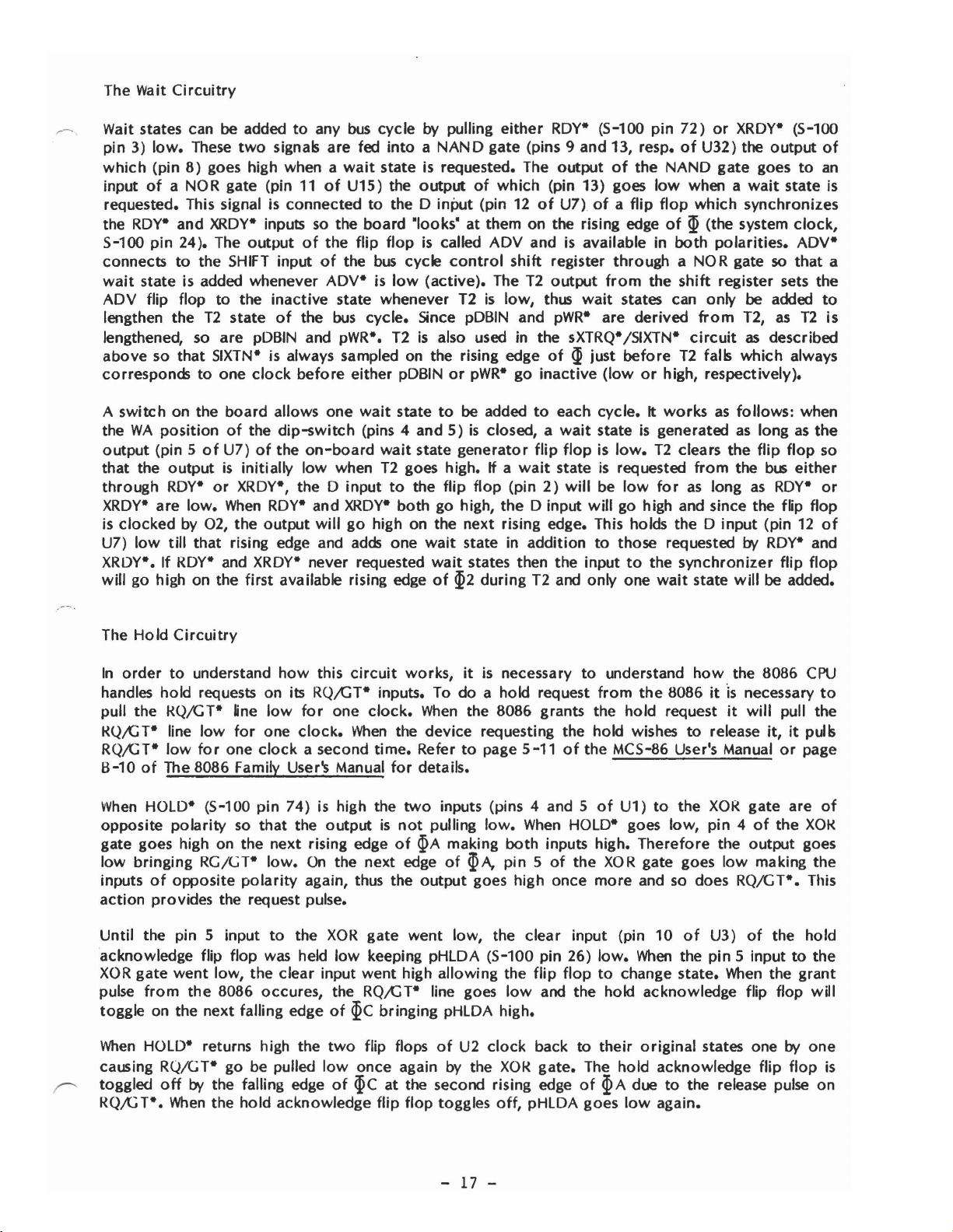
The Wait
Circuitry
,---.,
Wait states canbeaddedtoany
pin 3)
which
input
requested. This signal is connectedtothe D inPut (pin
the
5-100
connects
wait
ADV
lengthen the
lengthened,
above so that 5IXTN* is always sampled on the rising edge
corresponds
A
the
output
that the
through
XRDY*
is
U7)
XROY*. If RDY* and XRDY* never requested
will go high on the
low.
These
(pin8)goes high when a
of
a NOR gate (pin
RDY*
and
pin
24). The
to
state is added whenever
flip flop
switch
clockedby02,
on the board allows one
WA
positionofthe
(pin 5ofU7)ofthe
outputisinitially
RDY*
are
low.
low
till
two
XRDY*
output
the 5HIFT input
to
the inactive state whenever
T2
state
so
are
pOBIN
to
one
clock
or
XRDY*, the D inputtothe
When
the
that rising edge and
first
signals are fed
11
inputs
of
before
dip-switch
RDY* and
output
available rising edgeofID2
bus
cycle by pulling
intoaNAND
wait
stateisrequested. The
of
U15) the
so
the board "looks"atthem on the rising edge
of
the flip
of
the
ADV*islow
the
bus
cycle. Since pDBIN and
and pWR*.
either pOBINorpWR*goinactive
wait
(pins 4 and5)is
on-board
low
when
XRDY*
will
go
adds
output
flopiscalled
bus
cycle
(active).
T2isalso used in the sXTRQ*/5IXTN*
state
wait
state generator
T2
goes high. If a
both
high on the next rising edge. This holds
one
wait
wait
either
gate (pins 9 and 13, resp.ofU32) the
of
which (pin 13) goes
ADV
control
The
T2islow,
to
be added
closed, a
flip
flop
go high,
the
state in addition
states then the inputtothe
duringT2and only one
RDY* (5-100 pin
output
12ofU7)ofa
andisavailable in
shift
register through a NOR gate
T2
output
thus
wait
pWR*
of~just
to
each cycle. It
wait
flip
flopislow.
wait
stateisrequested
(pin2)will
D input
will
72)
or
XRDY* (5-100
output
of
the
NAND
low
flip
flop
of~(the system
from
the
states can only be added
are derived
before
(loworhigh, respectively).
worksasfollows:
stateisgeneratedaslongasthe
T2
be
low
for
go high and since the
to
those requested by RDY* and
wait
gate goes
when a
which synchronizes
both
shift
from
circuit
T2
clears the
from
as
theDinput
synchronizer
state
wait
polarities.
so
register sets the
T2,
as
as
described
falls
which
flip
the
bus
long
as
RDY*
fUp
(pin12of
flip
willbeadded.
to
state
clock,
ADV*
that
T2
always
when
flop
either
flop
flop
so
of
an
is
a
to
is
or
The
In
handles hold requests on its RQ,tCT* inputs. To do a hold request
pull the RQ/GT*
RQ,tCT* line
RQ,tCT*
B-10ofThe 8086 Family User's Manual
When
opposite
gate goes high on the
low
inputs
action
Until
acknowledge flip flop
XOR
pulse
toggle on the next falling edge
When
causing RQ/GT*
r---
toggled
RQ/GT*.
Hold
Circuitry
order
to
understand
&ne
low
low
for
one
low
for
one
clock
HOLO* (5-100
polarity
bringing RG/GT*
of
opposite
provides the request pulse.
the pin 5 input
gate
went
from
the
HOLO* returns high the
off
by the falling edge
When
pin
so
that
next
low.
polarity
to
was
low, the clear input went high allowing the
8086 occures, the RQ,tCT* line goes
go
be pulled
the hold acknowledge flip
how
this
circuit
for
one
clock.
clock.
a second
74)ishigh the
the
the
held
When
outputisnot
rising edgeofq>A
On
the next edge
again, thus the
XOR
gate
low
keeping pHLDA (5-100 pin 26)
of
~C
two
flip flops
low
once again by the
of
<t>Catthe second rising edge
works,itis
When
the device requesting the hold wishes
time.
Refertopage 5-11ofthe MC5-86 User's Manualorpage
for
details.
two
inputs (pins 4 and 5
pulling
making
of
output
went
low, the clear input (pin 10
bringing pHLDA high.
of
flop
toggles
necessary
the 8086 grants the hold requestitwill
low.
When
both
q)A,
pin5of
goes high once
flip
low
U2
clock
XOR
off,
pHLOA goes
to
understand
from
the
of
U1)
HOLD* goes low, pin 4ofthe
inputs high.
the
floptochange state.
and the hold acknowledge flip flop will
backtotheir
gate.
The
of
Therefore
XOR
gate goes
more
and
low.
When
original
hold acknowledge flip
~A
duetothe release pulse on
low
how
the 8086
8086it'is
to
release
to
the
XOR
the output goes
low
so
does RQ/G
of
U3)
the pin 5 inputtothe
When
states one by one
again.
necessary
pull the
it,itpulls
gate are
making the
1*.
of
the hold
the grant
flop
CPU
to
of
XOR
This
is
-
17
-
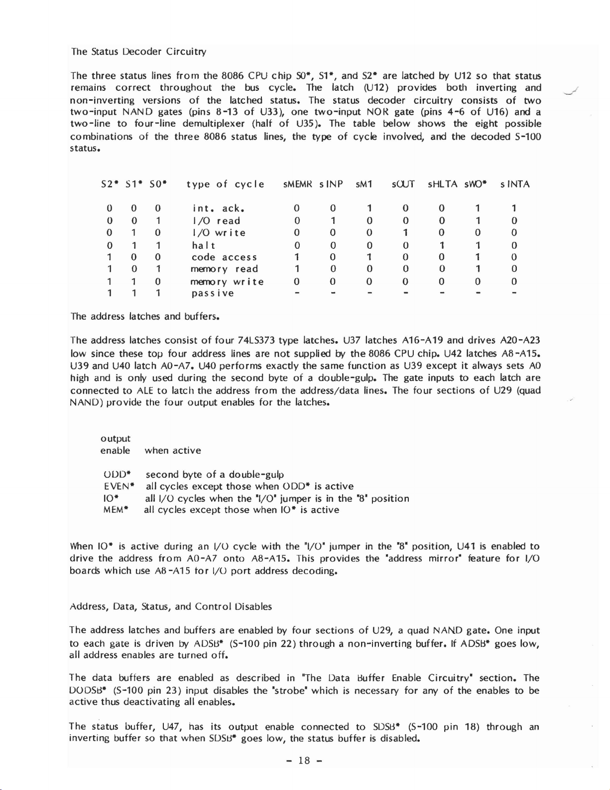
The Status
The
three
remains
non-inverting
two-input
two-line
combinations
status.
The address latches and buffers.
Decoder
status lines
correct
NAND
to
four-line
of
52*
51*
0 0
0 0 1
0 1 0
0 1 1
1 0 0
1 0 1
1 1
1 1 1
Circuitry
throughout
versions
gates (pins
the
50*
0
0
from
the 8086
of
the latched status. The status
demultiplexer
three
8086 status lines, the
type
in
t.
I/O
I/O
ha
It
code
memory
memory
passive
the
8-13
of
cycle
ack.
read
write
access
read
write
CPU
bus
of
U33),
(half
chip
SO*,
51*, and 52* are latched by
cycle.
The latch (U12)
one
two-input
of
U35). The table
type
sMEMR
s INP
0 0 1 0 0 1 1
0
0 0 0 1 0 0 0
0 0 0 0
1 0 1 0
1 0 0 0
0
1 0 0 0 1 0
0 0
NOR gate (pins
of
cycle
sM1
provides
decoder
below
involved,
sWT
circuitry
shows the
0
U12
both
4-6
and the
sHLTA
1
0
0
0
so
inverting
consists
of
U16) and a
eight
decoded
sOO*
1
1 0
1
0
that
of
possible
s INTA
status
and J
two
5-100
0
0
0
The address latches
low
since these
U39
and U40
high andisonly used during the second byteofa
connectedtoALEtolatch
NAND)
output
enable
000*
EVEN*
10*
MEM*
When
10*isactive
drive
the address
boardswhich
Address, Data, Status, and
latch
provide
useA8-A15to
consistoffour
top
four
address lines are
AO-A7. U40
the address
the
four
output
when
active
second byteofa
all cycles
all I/O cycles when the "I/O" jumperisin
all cycles
from
except
except
during an I/O cycle
AO-A7
r I/O
Control
74L5373
performs
from
enables
double-gulp
those when
those when
onto
A8-A15.
port
address
Disables
type
not
supplied by
exactly
for
with
the same
the address/data lines. The
the latches.
000*
10*isactive
the "I/O" jumper in the
This
decoding.
latches. U37 latches
the
8086 CPU
functionasU39
double-gulp.
is
active
the
provides
The
"8"
position
the "address
A16-A
"8"
19 and
chip.
exceptitalways sets
gate inputstoeach latch
four
sectionsofU29 (quad
position,
mirror"
drives
U42 latches
U41isenabled
feature
A20-A23
A8-A15.
AO
are
to
for
I/O
The address latches and buffers are enabled by
to
each gateisdriven
all address enables are turned
The
data
buffers are enabled
00050*
active
The status
inverting
(5-100 pin
thus
deactivating
buffer,
buffersothat
by ADSlJ* (5-100 pin
off.
as
described in liThe Data Duffer Enable
23)
input disables the "strobe"
all enables.
U47,
has
its
output
when
SDSU*
goes
enable
low,
four
sectionsofU29, a quad
22)
throughanon-inverting
whichisnecessary
connected
the status
-
18
-
to
bufferisdisabled.
buffer.
Circuitry"
for
any
505lJ* (S-100
NAND
gate.
If AD51j* goes
section.
of
the enablestobe
pin
18)
One
through
input
low,
The
an
The
control
manner
disable (CDSB·, S-100
as
the status disable
works
pin
19)
works
on the status
on the
buffer.
control
buffer,
U28, in
exactly
the same
MWRITE
The sOUT and pWR· signals on the
MWRITEisdriven
disabledifanother
read
The PHANTOM·
The
PHANTOM·ifdesired
CPU
nonextended-address
so
output
The POC· and
The
power-on-clear
the
power-on-c1ear.
power-on-c1ear
standard
wired
throughaschmitt-trigger
Circuit
from
the
bus,
four
top
address lines
addresses
that
this
circuit
and
thereforeifused should be the
RESET·
power-on-c1ear
'c1ock
circuitry'
power-on-c1ear
as
a 'pseudo
onto
pin
68
of
device
MWRITE
Circuit
memory
will
signals. The
C30isonly halfasbigasC29
releases
open-collector'
in the system provides
will
be valid
provided
boy
placing the 'PHAN" jumper in
above
memory
operate
Circuitry
circuitry
section.
in the
actually consists
first
The second
before
releases. poe· also drives
buffer.
bus
the
the
for
comes
the
any
driver.
(pins 45 and 77, resp.) are NORed
bus
and goes
no
matter
by the 8086
first
64K
first
64K.
bus
master. Also
only
from
uses
other
one so
RESET·
through
MWRITE.
what
(A16-A19)
the
PHANTOM· line
Notice
PHANTOM·
of
two
R5
& C30 and resets the ring
R4
while
R4
that
RESET·
drives the
the
Notice
bus
master
are NORed
the
'+'
position.Inthis way, whenever
that
the
source
notice
driver
seperate R-C
& C29 and
and
R5
the
clock
through
RESET
"MWRTE"
that
provides
thatitis NOT
in the system.
are the same size, thus the
together
jumper so
since sOUT and
sOUT and pWR·.
together
will
be
for
A16-A19
networks
provides
is up and running
one
input
to
activated
an
to
counter
the standard system
section
to
the 8086
form
MWRITE.
thatitcan be
pWR*
and can
is the bus
open
provide
described in
of
a 74LS125A
to
disable
collector
before
CPU
drive
itself
two
clock
chip
are
the
the
- 19 -
IEEE
STATES
8086
STATES
<1>
A
<1>B
<1>C
<1>
(8086)
BUS
"T
.
BS1
8086
"
I
I
!
I
T1
I
I I
I I
I
8086 T2
I
I
BS2
I
I
I
I
I
i
I I
i
8086 T3
BS3
8086Tw
I
I
I I
i
I
I
I
I
I I
I
r
I I
r
<1>2
SO-S2
LOAD
U5-6
ALE
TO
T1
T2
T3
.,
pSYNC
pDBIN,
pWR
\
I
l
I
I
I
I
I
I
J
I
I
I
ODDBT
ROY
WAIT
DONE
U23·5
I
I
I
r
I
i
i
I

3086
T3 8086
I
BS3
I
Tw
8086
Tw
I
I I I
BS1
8086
I I I I I I
Tw
BS2
8086
I
I
t I
I
I I
Tw
I
I I I
J
; I
I
BS3
8086
T4
I
I
I I
I I I I I I I I I I I
I I
I I I I I
!
I I I I
I
/ \
I I
I I
I I
I I I
r
--
~
-
I
I
I I
I
L
-
\
I
i
I
I
I
I
i
I
i
I
I
!
- 20 -
I
I
I
I
,U.St:T
v
+r
<.z.
t!D---t~
; g
R~
3{,
q
2-11>1
.,~OI~
DH
,,,"A
,-
•
_"
~'~
c""
..
30
"7
......
~I·i;::.
(C~
R"
-
~a
'1.jo
q[.,
lla.~~
'¥Z
I~
~
l!!L.J.....
/4
1
- - I
..
'11V'\1\1l..
.,p
--
k--~"
'lilt·
)L
• ..,J
HV
J
27
1.
~
~
rh
_.
~
or
/1
..
[1'2">
7<4L.'szo
+r
•~'.I
!4
,~
~2.
1'P1
H>l
,P}
tp
..
TPS-
AI{,.
AI1
AI'1
AI'l
!
R5
I"
~
+
(3~
-::-
T''1~F
-=-
')
I'
H
1.I
lIl>
I
r~",l,
'Il-Lr:.
111
Nr11
181
tN't~
LO(.~
qs,
~
"",IS)
"11
I
Qn}-:'04
~
A,s/Ss
~
~~
A"';'-!f"
Z'
~
27
I
~
a
r
'It
~
,.
v34
BoB"
'!:r'
·
~
+S
~
L L
..
R'~~(,rr"
__
:t-~1-~~'
t\tltS"
Abl4
Abl1
ADI't
AlllI
ADlo
AD'l
A~
ft
Atx.
l\tt~
fl~
AD)"
J\'t>~r-I\tlt
Jlt>l~'L_~
;:r
A.6V,r
w·"
~
t't>,
_
--
~
~
t>,..
A011
AOI~
Atil
Ab8
A~'7
~b!.
AH
A""
~'\)3
A}l
1-
~
4
.--tlbl't
'i
'-"f\Oll
c.
1
II
.•.•.
b7
'1
ro
I'
p-1.
Ab_~l\tJ~
d1
L--------.
.
··'·~·~lST1~
l)
'7
b
'·'(~·-l
q,
I
2.
~
Q,
- '-
,l.1. L
1.2.
q I
~
~,
n.
I
II~~II
.s
t
AY
----1°
1
-~:
- . 10
.QD---L
r.
r.
I
(~
C
...
....
;;
-l
<r
..J
c.
I
LJ
"',
r
~,
....
...
wi
..
do
3
0-
~
f'
c
""
~
~
~
~
a....
~
i=
~
--
....,
(l'\
2
4-
7
~
I
~
V
VI
(0
">
11
~
r-
I
-
-
,
,.....
U.
0
uJ
~
J
Q.
\J
19
~
<r
a.
",
.'
"'Q.
1'1
~
t~~
."..
fr
'!:
.".
...
.,
..
..,..
~
"c41
'"1
N
lP
I
"
~
....
Clt
~
~
I'
N
"
-&-
"'"
j
,.
.,
...
c
...
'"
,.,
V
C
....
....
l.n
:ll.
.-
'"
a
.,.
J
..
...
C
..
l.U
c
...
%
.;;
Q.
Z
0{)
..
'>
~
co:
0.1'
~
.J
r,
/1
....
's:
11\
..
~
oJ
0
~
r(
In
t"1
et:
cD
'!:
~
~~
1-
'I'
~
r-
S\
..
0-
...
I~
T
r;
fi:>
'&
""
J
....
o;t
~
....
1:
VI
~
I~
I~
~
+-<3
t
q
"'~I:'
~
01
0-
It
'"
...
'"
oJ
.....
v-
,...
r<'
-I
'"
....
I-
)(
I{)
$
<r
'"
'"
I-
rt
z.
II
"&
c
...
10'
on
10"
0
::r
j
c
"
a
r-
m
~
IV1
P
~
I~
G
I~
,-J
. :
."
'3~'
PO(..~
14
.
1'1
~B3>-._~'7
(1
M1
U)
.,.\"
~
1\~2.
f
16..-
1'1
\~
..
18
.fj
"
--1"1
- f-..'----.---
II>
.
T
tS
P.l }
~j(,
i
Ie:
3>,u.F
_.
0'"
.!~r-.f
/5
11.--
IZ~'
_
i"Z.
10
(.(
~Atl"
1_1
8
7
~~
I}
"
~
/0
~J:
-oj
1l-<»~
14
I .
I
"WI
"¥i
'
I'S
1.1
'ft1"yJ
_~/O
-
13f
II
~)(T
L
p.'1,
-4
35"
/J(.
/1
1
32-
ffC
6
,
,-;.
~5~'1
R-S
1?",SI)~
JS
I>
t
1 I 1
"
(,c.
u:
,,~
-
'A
t !
J
3
r~~c.~t
'9
-I
10
LO"l)
~""T
-"-.-""
.J.
.
0\
~
1~--'r
T~
Tl
!1-11.
S
1'\
<..
11'\
b
·-1'
T2
0
~Li
:Cll.l\.
--,'t'
T1
IN
l~
I.,
b
Q.
/¢
1
"1
wo~ilp
T9
13
1 3
1'3r~
I C
'1'
::>.,
I q & I
I
- - -
cf1..
It+''"
lt1
"'
l
':
Q.
S2¢
_1/'1
- I
ir
tS'
f
I~
,~
I
12
'
'il~pw",
:n.
pWAlr
~
[21>--_?
.\"
I.1J'2..
!
I~
2.lf
fJA~
--
I S
I
RQjr,f
'5
'1
g
J
Gl
Cf
z
n.
-----
'1'-
OISlllh{.
..)
~
"
...J
""
..
....
N
I"'
~
':!"
,...
~
\[-,
In
I'
("l
('
C""
'l'
~
....
,...
I'"
~
~
~
"=
0
{'l
~
<.
~
N
ry
I
':1
o.
!::
c
h "i=I
Le..J
-
"T"
~
4.
~
cs:
p
C-
C'
~
d::>
~
c::
a:.
n
.-------------
t
I
I
-
~-_.
•
'M_"
,
.
"-'
-,
I I
.._.....-_.•
I·.,
---
..
---~
.-----.<!!J
...--....
_--~
<§]
-
~
~t>t3
---<Sl
~
1)t.7
b r "
t>t S
b!
bl"
~1.
vI.
~
I
P
I'O,t
~~
~b
fWt)1't
"tll\
~\O
~l)q
,,~
PAGE
lH
..
~
0"13
3
17
I)
,e
'1
I~
I~
-..--_._--
-
'-----
.._----.--_.---
.-"-
---..--.---.
Z or:
Gb8~
II
fV\
~",N
....
-----..
Z-
CPv
f'fl<;~~e-(',/
31",
/Cf7'!
~
-.--<~
-
-----qiJ
-~
~
<n;
AI'S
~
14
"I,
"1'2.
F\
I I
"IQ)
..,
-·-·~A~
~
1>
-'~f\B
-----_._---
..
"t"
J..f
i
~
~
;t
P'
1/3
12
lGo
7
74L-":."3
I
I
I
!
J
I
I
..
_~._--
._--
I
A~l
~~~
~b3
~~'"
!
7
I~
n
&_~
)
I-~
~~--rr1-o
--r-.-t--t-_·
i I I
:-----+,-<.jTI-t--TI
I
11~.
Q.
. I T
----
·--T--t--\-·---t
I/? h
-
.t
I~
! I
L.
1
I
.
_.-
.
__
.-.-
<@~1
::::
--_.-~
-.-
----<D]
-
---....<.&!J
Pt~
~~
"J
f\
'2

'13
7ItV/L
J.A
1\1>1
so
----~-~---
-
r-------
-_
...
_-
~Do7
I;b1
ftb(, --:...:.....,.
-
ll{l
~
~(S
0
,-
/5
~t.IA
/lib
13
Hbl'l.
f\~I'
---,/--11»
"blP
Abq
At>
g
__
At>'
l\bS - I
flt>'t
(;,
I
7
I
b d
1'1
2.
r.-{
~
.1
/b
1
I~
rb
~
3
f;
1,11
17
I~
l.o\L-"J1.<\S'
r;Q
--------
.
I
I
-.----_._------
-:l-;
: .
r-t-
I
;
-1---
T
---
---~
--~
~--l--+'--;~
I
:_+
I
I
_L
I
f
__
."f._-+~_
•
I
!
bof,
ros-
<1!
l>04
<li
!Jo~
Q!
1:>02
~
hOi
c::;
'bo
p5
A~t>n..
~Sl!l..
"1)
~
1>
1.
¢
DlIlIor
~
'1
~
r-~
I I I ,
rt>
~
~
Q
LS1
ellb
"
lr-=-=---
1/0
f<ll
8 "
f--o[
...
"
.....
I
"~3
""1
::;
'1
I
!;.u
3 FI I
--5""-~t,:~:i
I /9
LSi
11'1
81
I'
~/7
"_
(De
I i
~
,
\
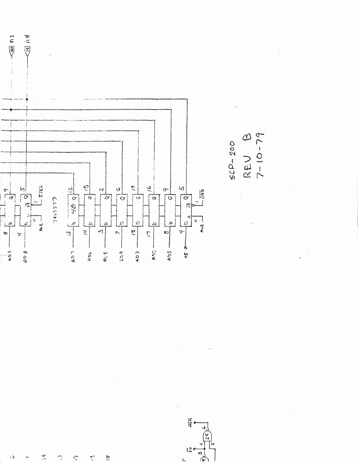
--
i
-
..
~
-_
..
-.
--
--------------.,
..
_;
-+---+---------------------.,
_....----
--...
8=
:.
i
---.-_.
I
I
-
-_._--
...._---_.------_._---.....,
--------
-----------,
. 1-----·--.
i
~
r;.
':':1
Ie)'
D
IIf)
~
-
r
oJ
P
C'
et
<l-
r-..
U\
i.'
~
'"
D
C'
~
l""
<T
P
P
-.-'
<£
c-
dJ
:>
ijJ
C!
('-
,
0
I
r'
o
0
'"
I
a.
~
\()
l/}
\}-
C)
~
::
Q
~
IJ
~
~
r-
-
r'
I-'
"'"'
P
4:
4:
~
III
...
«.
I~
'
....
.....
l~
10.
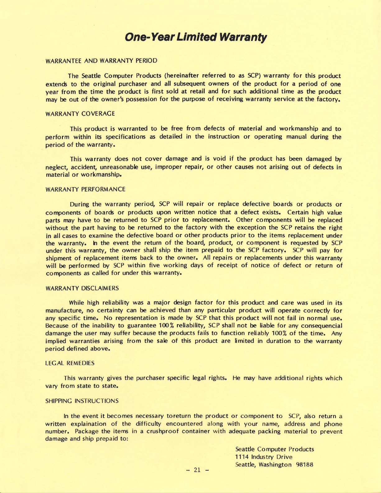
One- Year
Limited
Warranty
WARRANTEE
extends
year
from
maybeoutofthe
WARRANTY COVERAGE
perform
periodofthe
neglect, accident, unreasonable use,
material
WARRANTY
components
parts may have
without
in all casestoexamine the
the
warranty.
under this
shipmentofreplacement items backtothe
will
be
componentsascalled
AND WARRANTY
The Seattle
to
the
the
This
productiswarranted
within
This
warranty
or
workmanship.
PERFORMANCE
During
of
the
part
warranty,
performed
Computer
original
time
the
owner's
its
specifications
warranty.
the
warranty
boards
to
be returned
havingtobe
k1
the
by
PERIOD
Products
purchaser and all subsequent
productisfirst
possession
does
not
cover
period,
or
products
to
returnedtothe
defective
event
the
for
owner
SCP
within
under this
the return
shall ship the
(hereinafter
soldatretail and
for
to
be
as
detailed in
damage and is
improper
SCP
upon
SCP
prior
boardorother
of
five
working
warranty.
referred
owners
the purposeofreceiving
free
from
defects
the
instruction
repair,
will
repair
written
to
factory
the board,
item
owner.
or
or
notice
replacement.
with
products
product,
prepaid
All repairsorreplacements under this
days
of
to
of
for
such
of
voidifthe
other
causes
replace
thatadefect
Other
the
exception
prior
or
to
the
receipt
as
SCP)
warranty
the
product
additional
warranty
material and
or
operating
product
defective
to
componentisrequested by
SCP
of
notice
serviceatthe
not
arising
boards
exists. Certain high value
components
the
the
items
factory.
of
for
this
foraperiod
time
as
the
workmanship
manual during the
has been damaged by
outofdefects in
or
products
will
SCP
retains the
replacement under
SCP
will
defect
or
product
of
one
product
factory.
and
to
or
be replaced
right
SCP
pay
for
warranty
return
of
WARRANTY
manufacture, no
any
specific
Because
damange
implied
period
LEGAL
vary
from
SHIPPING
written
number.
damage and ship prepaid
DISCLAIMERS
While high
time.
of
the
the
warranties
defined
REMEDIES
This
warranty
statetostate.
INSTRUCTIONS
In
the
eventitbecomes necessary
explaination
Package the items in a
reliability
certainty
No
inabilitytoguarantee 100%
user may
arising
above.
gives the purchaser
of
was a
can be achieved than any
representation is made by
suffer
because
from
the
to:
major
the sale
difficulty
crushproof
design
reliability,
the
products
of
this
specific
toreturn
encountered
container
factor
SCP
failstofunction
product
legal rights. He may have
the
for
particular
that
this
SCP
shall
are
product
along
with
this
product
product
product
not
be liable
reliably 100%ofthe
limitedinduration
or
component
with
your
adequate
Seattle
1114 Industry
Seattle, Washington 98188
- 21 -
and
care
was used in
will
operate
will
not
for
additional
to
name, address and
packing
Computer
materialtoprevent
Drive
correctly
failinnormal
any consequencial
to
the
SCP,
also
Products
time.
warranty
rights
use.
which
return
phone
its
for
Any
a

 Loading...