

Page 1
·...
,I
~
J
ST225
-
OEM MANUAL II
PLEASE NOTE
SPECIFICATIONS OF THE ST213 HALF HEIGHT
10MB DRIVE CAN BE FOUND AT THE BACK OF
THIS MANUAL.
f
.I
, c'o._•. ~•.. H_W" ; _.",..'_, ', _, _ • '. ,_. _..:. ••• ;": •• ~':';::. ;••• ,', ••••~.:i-'...,--..•.;~;l7''t~;~':'"t:.;".:.."••.•_:".'' ."!,;,,;~,,,-,~,,::;,;,,_~,,,",..;,c.~':-:':;,:~':'i:";...!'~::":~";.'~~_:••.~;_L·..;', '~"'~'':';';'-:''i-',!~~ ~.,;..::; ....~.:'~;~ '::",.. ,..:. ,~_.-
• t •••
95066-4544,USA. 408/438-6550
'y,
--
Seayate I]
~ --~~':':!.I~
I]
~II
Page 2

"
Page 3
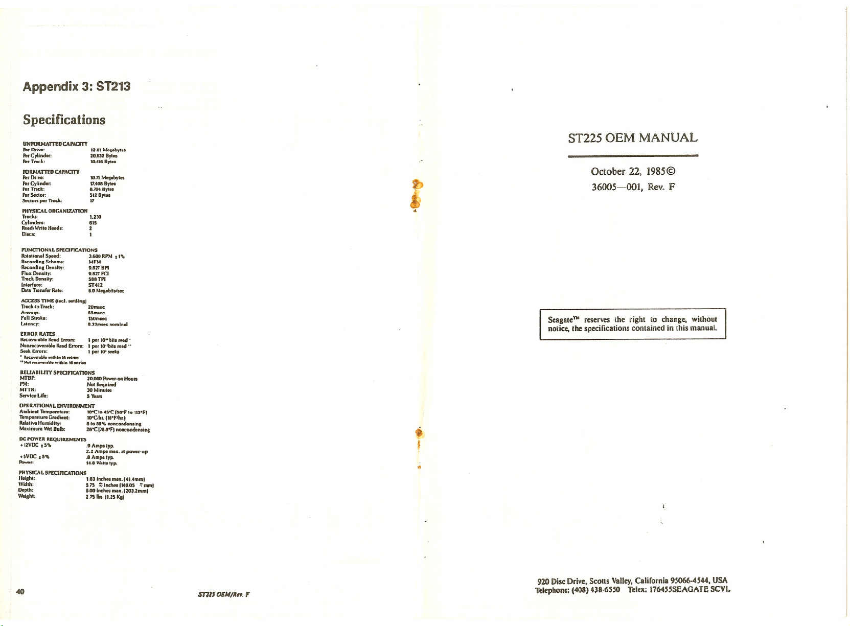
Appendix 3: S1213
Specifications
UNroltMAmD CAPACITY
Pet Driw:
~rCrlindor.
•••• Trocl.:
roRMAmD CA'ACT\'
Per Drtw:
P.rCylindet:
An Tnc:k:
IW SectOl':
SeetON per
lrKk:
PHYSICAL ORGANI7.ATION
TrKu: t.210
Cylinden: 815
Red/Write He•••• : 2
DIK': 1
fUNCnONALSP£CnCATIONS
Rot.honlll Speed: 3.600 RPM
Record!n. Scheme: MFM
Recordihl Den.U,: '.827 BPI
Flu Den.lty: '.827 Fa
TrackDen.II,: 588TPI
Interface: ST412
o.'a Tr.Mr., tt.,.: S.O Mes.bUslleC
ACaSS TIME
1rKk·lo·TrKk; 20mMIC
Aver'lIt8: aSmRC
Full Strub: UOmaec
Lalency: I.JJmsec; noml •••1
EnOR RATES
RKowf.bI.
Non.rtICowr.W. RlrIHf Enon:
Seek Erron:
·1itK.~~wHhlll"ret""
u No4I NCCftIftlbie ."hlll •• ,.., ••
REWlnsrY S'WnCATIONS
MTBf: 20.000 A7wer~ Houn
PM: Not Requhod
M1TR: 30Mlnul••
SeI'YlceU": S
OP£RATIONAL ENVIRONMENT
AmbMtnI1empefllturo: ttrC 10 45"'C ISD-Flo 113-F,
Temperalure C,.ch.nt:
Rel,liw HumidUy: • 1080'" nonconden.lnl
Maximum Wet Bulb: 28'1: 1'•.•
DC!'OWU REQUIREMENTS
.IZVOC f: 5'" .1 AmIN 'yp.
• ,VOC
PowItr: 14.11
PHYSICAL SP£anCATIONS
U.lahl: 1.131nchet ma•. lfI..mm'
\Vkllh: S_lS = Inchet 1148.0S ~ mm'
Depth: 1.00 Inc:hee mu:.1203.Zmmt
WelSh': US II.. IUS kal
lIad. -U •• ,
ReIHl Enon:
t,•••. 1 Amptlyp.
12.1' Mea_byt"
20.'32 Bytee
Xl.416 Byt ••
Moa.by1"
MJ.n
11.4088)1"
•.••048)1"
512 8y1"
"
t''''
1per H)-bll. ,ud •
per lO'tbit.rv.d··
I
J per to"seeb
'lean
1O"'Cthr. (1S·''''r.1
·'1nonconden.lnf;
2.2 Ampl
mall .•• power·up
W.'IJIYp.
Ii
f)
{
.•
~
ST225 OEM MANUAL
October 22, 1985©
36005-001, Rev. F
Seagate'" reserves the right to change, without
notice. the specifications contained in this manual.
J
t-
920 Disc Drive. Scotts Valley. Calirornia 9S066-4S44. USA
040
mlJ OEAl/~",,
Telephone: (408) 4)8·6SS0 Telex: I764SSSEt\GATE SCVL
Page 4

o :-:-
..
-""\oOD
!!.;O 0
:; ~~
",,'
eN •••
N-Uil UII
n"
g ":':1
n
S8~=
ell
0
~
';- tii°
fA
••
Q,
@
"'I
-
...•
W
m
::Iaaa
"CI
"C
~~~§
fJ)
-...
C'''''
.. ""
:;==
~g
Q.
~
;C'
CJ)
"C
"t'J
Q)
::::I
W
Q.
>
:=
(I)
.,~
3:11I..,..,
""'.
I'
Page 5
·,·.· ....'4..-.....~
~,o.~ .•..,:.•.••:.•.•.\...
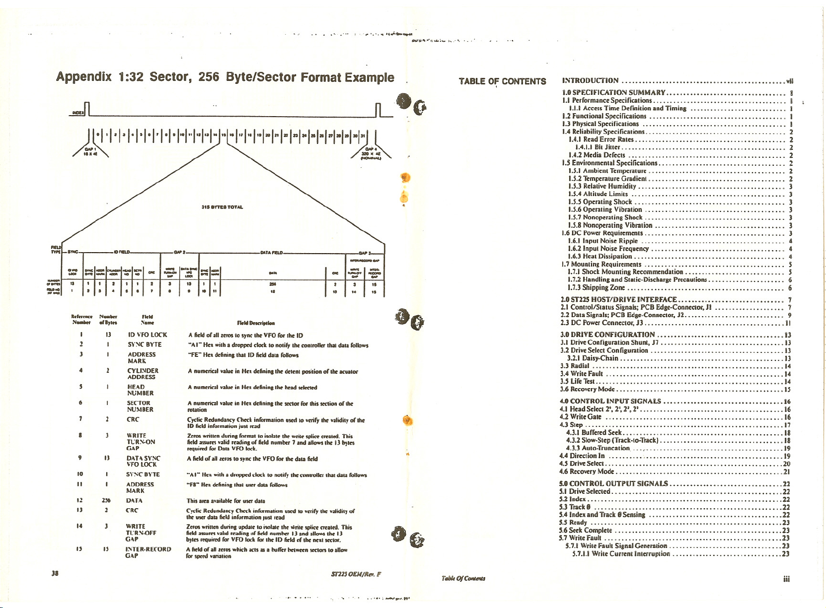
Appendix 1:32 Sector, 256 Byte/Sector Format Example
~ ~fLOO
A:~I·I·I·I·I·I·I·I·I·H;tJ·~1·1·1·1+1·1·1·1·1·1·'jj~~
315 Ims TOTAL
'::
=1=
:=1--;;
-..•
..-
IdHNn N_1N<r fleW
N•• 1N<r eI.,ln s.rnt
4
6 I SECiOR
9 IJ OAH SYNC
10 I SYSC BHE
II I ADDRESS
12 256 O-\T..••
IJ
14 J WRITE
" " 1:o;rER·RECORD
II
-:Ol~
IJ ID \'FO LOCK
I SY:-IC BYTE
I ADDRESS
MARK
2 CYU:-IDER
ADDRESS
HE.-\D
NUMBER
NUMBER
CRC
WRITE
Tt: R S·ON
GAP
\'FO LOCK
MARK
2 CRC
Tl: R:-I'()ff
G-\P
GAP
....,
I\-.cIIIt IIfO ent_
- ....
-1 •..'.•IftCIPCI••••
tI I' I'• It tI
A field or .1I,etOS 10 sync lhe VfO for lhe 10
••AI"
H•• wilh • dropptd clock 10 nOliry lhe conlrol •••.lhal dal. "IIOWI
Hex dtfinin. Ih.1 10 Mid dal. follows
"Fr
A nu••••ric.1 •• Iu. in Hex dtfinin. lhe dtl.nl posilion or lhe lCualor
A nu••••ric21•• 1•• in Hex dtfinin. lhe hoad ••lcc1ed
A num.rical •• Iu. in
rotation
Cyclic Redundancy (1)<ck inrormalion uoed 10••riry lhe ••Iidily of Ih.
10 fieldinrorm'lion juS! ••• d
lam wrinen durin, format to isolale the ViniC' !Plitt (~;litd. Thii
fielda$SUm •• Iid ••adin. of field numhor 7 .nd .11owslhe IJ 1»1<5
r<quirtd ror Dal. VfO lock.
A field of .11'''0110 sync 1M VFO rot lhe d••• fitld
"AI" H•• wilh • dropped clock 10 notiry lhe con,roIk, lhal dall rollow>
"fA"
H•• dtfinin. lhai UKr clata rollow,
This am .,waibbk for UKr Ibl,;
Cyclic Redu ••••ncy Check inrorm.,ion uKd 10•.nry lhe •• Iidity of
the UKr data Mid informillion JUst read
Z••OI wriuon durin. updol' to i•• I.lo tho writ. splitt eft.,td. This
field '$SUm ••Iod••:odin. IIr field oumher lJ.nd .11owslhe IJ
byl•• '«Iuired rot VfO lock rot ,he ID fitld of lhe ••• 1 KC'ot.
A fitld of.II •••.01 which acts II •bulf•• Ioti"un •••• 0<110.11_
for ~ "'arialion
MTA f1ELD
"'::'
tI
,
.•.•
".
"
floW Dnnl" •••
H•• d.finin. lhe •••• or rot Ihi, ••••ion of 1M
-..
...•..
--
tI
3tI
••
""::'"
.~
,
•..
~o
~
o~
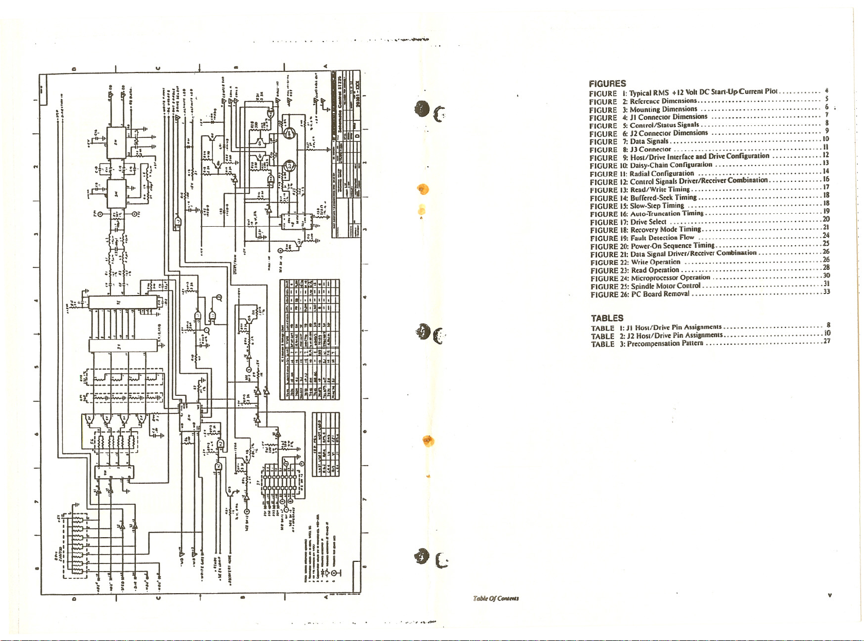
TABLE OF CONTENTS
I:'WTRODUcriON •.••••••••.••••••••••••••••••••••••.••••••.•••••
i.OSi'ECiHCATiOS SUMMARY •••••••••••••••••••••••••••••••••.• 8
1.1 Perrormance Specificalions ........•.•.••••..••.•.•...•...•••....• i
1.1.1 Access Time Ddinition and Timins .•.••..•.•..•.•..•...•..••.. I
1.2 Funclional Specifica.ions .••.•.•••.••.••••.•.•..•..••.•.•.•.••••. I
1.3 Physical Specificalions ...•..........•.••••.•..•..••..•....•••... !
1.4 RtiiabililY Specificalions ..........•...••••..•.•.•.•..•••..•.•••.. 2
1.4.1 Read Error Rales ....•.......•.•..•••••.•••.•....••..•.•..... 2
1.4.1.1 Bil Jiner •....•.....•......••..••....•.•.•...•..•......•. 2
1.4.2 Media DereCIS ••••........••.•.••••.•..•.......••••..•••.... 2
I.S Environmental Specifications ...........•••...........••.••.•.••.. 2
1.5.1 Ambien. Temperalure ..........•..••.•...•..••.••••..••....•. 2
1.5.2 TemperaiUre Gradi.ni. ......•...•...••..••..•..........•.••.• 2
1.5.3 Relalive HumidilY ......•..•.••......••.•.•.•.•..........•••• 3
I.SA Ahilude Limi.s .........••......•••.••..••......•...••.•.••• 3
I.S.S Optrating Shock ....•....••.....••••..••......•.••••••.•.... 3
1.5.6 Operaling Vibralion ........•.....•...•.••......••...•..•..•• 3
1.5.7 Nonope,ating Shock ..•...•.•......•......•.......•..•..•.•.. 3
!.S.8 Nonoperaling Vibralion ...........••.......••....••••••••.•.. 3
1.6 DC Power Requiremenls ...•.....•..•..••..•.•..•..•....•••...•.• 3
1.6.1 Inpu. Noise Ripple •....•..•.•....•.....•.•••.•.....•.••..•.. 4
1.6.2 Inpu. Noise Frequency •..•..•....•••••...•.......•.•..•.••••• 4
1.6.3 H.al Dissipation ••...•••..•.•..••.•.••.•••..•...••.••.•...•. 4
1.7 Mounling Requirements ...•.....••.••.•.•.••••.•.•.•••...••••... 5
1.7.1 Shock Mounring Recommendalion .•••....••...•.•....••.•••... 5
1.7.2 Handling and Slatic·Discharge Precautions .••.••......••.•.•••.• 6
1.7.3 Shipping Zone .•.....•......•..••.••...••••.....••..•.•..•.• 6
USn25 HOST/DRiVE INTERFACE ••••••••••••••••••••••••••••••• 7
2.1 Conlrol/Slatus Signals: PCB Edge·Connector. JI .•..•...•••••.•....• 7
2.2 Dala Signals; PCB Edge·Conneclor, J2 ...•••..•...••.•...••••..••.• 9
2.3 DC Power Connector, J3 .•••.....•..••.•..•.•.•...•.....••....•.. II
3.0 DRIVE CONfiGURATION ••••••••••••••••••••.•• , ••••••••••••• 13
3.1 Drive Configuralion Shunt. J7 ..••••.•••••.••••••...•.•.••....••.. 13
3.2 Drive Seleci Configuralion .•••.......•.•••••..•..•.•.•.•.••..••.. 13
3.2.1 Daisy.Chain •...•••.•...••.•..•.•.•...••...•.•...••.•••..... 13
3.3 Radial ..•...•...••....•.•..•.•..•.•...•••••.••.•.•••.••.•..•.. 14
3.4 Write Fault ....••.•••...•.•.•...•.•.••••.•..•••..•...•••...•••• 14
3.5 lire Test. ...•.•••...•....•••..•.....••••...••..•••.••••.•.••••. 14
3.6 Recovery Mode ••.•.•........•....••..•..•..•..•...••••.•.••.... IS
4.0 CONTROL INi'UYSiGNALS ••••••••••••••••••••••••••••••••••• 16
4.1 Head Seleci 2", 2'. 2'. 2' ..•...•.....•....••.••••.....••..•...••..• i6
4.2 Wrile Gale •.......•....•......•.••..••..•.•......•.•••••..•... 16
4.3 Slep ....•.....••...•....•••.•..•••••••.•.••.•....•....•••••••• 17
4.3.1 Burrered Seek ..•..•.•.•.•..•..•..••••.••••.•.•.•.•••••.••••. 18
4.3.2 Slow·Slep (Track-Io-Tr:ack) .••..••••.••••.••••.••.••..••.•••.•. 18
4.3.3 AUlo·Truncation •.. , •....•...•.•..••.•.••••..•.•.••.••.•.••• 19
4.4 Direclion In •....••.•• , •.••..•..•..•••••..••.••..•.••.••.•..... 19
4.5 Drive Select. ......•.•••....••......•••.•.•....•....•..•..•.•••. 20
4.6 Recovery Mode ...••••......•......••••.•.••••..•.•..•.••.•..... 21
5.0 CONTROL OUTPUT SiGNALS ••••••••••••••••••••••••••••••••• 22
5.1 Drive Selected ....•..•••...••.....•...••.....••••.•....••••••.•. 22
5.2 Index ..•..•.•...•••••.•....•....••..•.•••.••..••..•.•••.••..•. 22
5.3 Track" .....•..•.......•.•......•••••••••.•....•.••.•.•••••..• 22
5.4 index and Track" Scnsinl ..•..•...••.••••.•.............•..•••.• 22
5.5 Ready .•..•.•...••.•.•..•••.••..••..••...•.•....•••....••.•... 23
5.6 Seck Complete ...••.•..•....•.....•..•••.•.••.•.•...••.••.•.••• 23
5.7 Writc f~uli ....•................•..•••••..••••........••.••••.. 23
S.7.1 Wriie fault Signll <lener.iion ......••••.••••...••...•..•..••.• 23
5.7.1.1 Wrile Curreni imerrupiioli .......•....•...•..........••.•. 23
'On
JI
mlS OEM/!lIf'I. F
,
..•.~-•..... ".
TJJkO/C_mu iil
Page 6
j.8 Faull D~t~':lion ., , , H
5.8.\ DC·Um'al~ Si8n~1 ~4
'.8.1.1 VoUla~~ Comparalor., ,
'.8.2 H~ad Select Comparators ., ............•..................... 24
6.0 powt:R·B.\ SF.Ql'E;I;n: .•..•...........••....•••..••••••• :: ... 25
7.U UATATR.",;I;Sn:R U;I;t:s ...............••..••.•.....•••.....•. 26
7.1 WrileOper.ation., ......................•....................•.. 26
7.1.1 :\IFM \;vrile Data .............................•......•.•..... 27
7.\.2 Write Gale, .....................•....•........•......••.... 27
7.1.3 Line R"'cei\'~r . , 27
7.\04 Precorrnpensation ...........................•.......•....•... 27
7.2 R~ad Ope ••:"ion 28
7.2.\ M F~I Read Dala .............•.•...........•.•......•....... 28
7.2.2 Head Select 28
7.2.3 lSI Preamp , .................•..•..•....•.............. 28
7.204low·PatsS Filler ..................•........•..........•.•.. · .28
7.2.5 Phase Shifr~r 28
7.2.6 Z~ro·ClosS DCICclOr , ................••.................. 29
7.2.7 Time I>omain Fih~r ..................•.....•................ 29
1.2.8 Line Du-h'er ............................•.................. 29
1.0 TlIt:ORY OF OPERATIO;l;S .....•.....•..•......••.•.••.•••..•• 30
8.1 Microproc~sor .................................•............... 30
8.1.1 MPU·h,ilializing ............................•....•..•...•••. 30
8.1.2 MPU-Itdle ......................•.................•......... 30
8.\.3 Seeking: , ........................•.......................•.. 31
8.2 Spindle M01er Conllel .........•....•...•.............•.......•. 31
9.0 fIELD SERVICE ....•••...•......••..••.••..••••.••••...•....• 3J
9.1 PC Board Removal ....................•..•..................... JJ
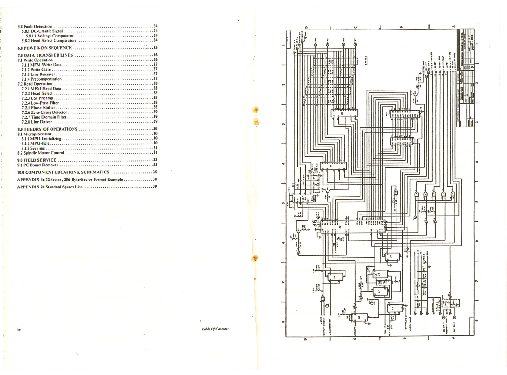
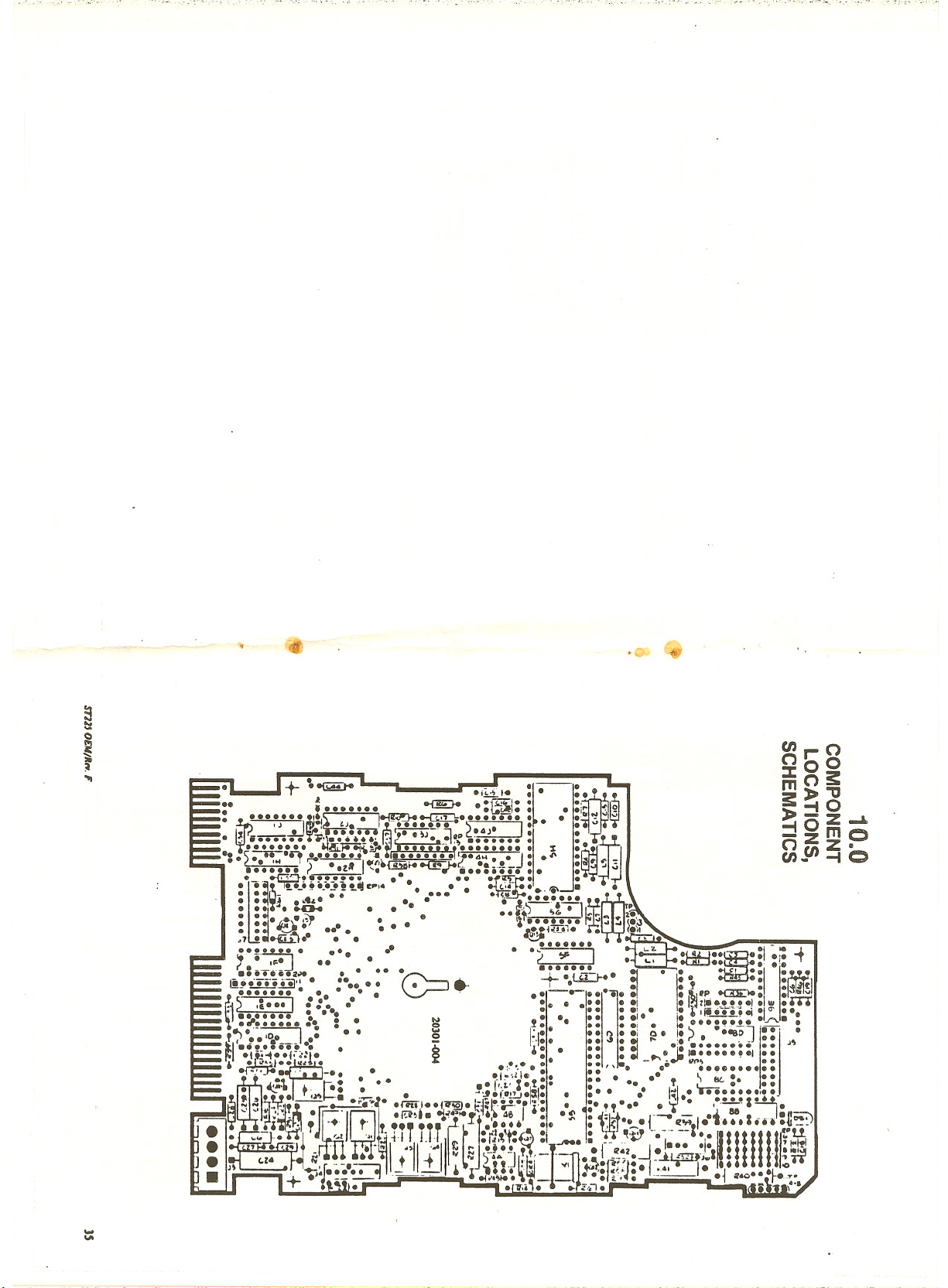
10.0COMPOSf.:\T LOCATIO:\S. SCm:MATICS .....•.......•.•...• J5
APPE:IODIX
APPE:-IDIX 2~ Siandard Spares List. ..........••.......•••.........•. 39
I::J2Srclnr. 256 D)'le/Se<lor Formal Eumple •....••••.•••• 31
u
c
H
ElmMB
;~lft~l_
J
m
"
~,-
..
,~
~
..
;,
=!}
IH:
I!':
:!
:.I
l
~11I111,a
111t
IIII
I!l11!m~
i
I
II.•
..
it:::::::....
•
!H",!
"
~
..
.
.
iv
\,
T,,}II,OfC ••••
rnNl
o
I
~
u
, :J:
;":
;
•
c
•
..
•
Page 7
. ' -..•....""
G
·
·
..
• f':I!':r~
u
.
:'
i
,.
..
!!
.
.•
I • IIIIII
I tit i. III
••
'I~'
if'
-,-
e(
'()
.•
e(.
FIGURES
FIGURE I: lYrical RMS + 12Voh DC Slan-UpCurn:ni Pial .........•.. ~
FIGURE 2: Reference Dimensions •.•..•.••..••.•..•...•...•.••..•.•.
FIGURE 3: Mounling Dimensions ...........•...................... 6
FIGURE 4: JI ConneclOr Dimensions ......••.•..................... 7
FIGURE S:Control/S.alus Signals ..........••...................•.. 8
FIGURE 6: J2 Connector Dimensions _................•.•... 9
FIGURE 7: Dala Signals .................•.. _ 10
FIGURE 8: JJ Conneclor ....•.............. - II
FIGURE 9: HOSi/Drive Imerface and Drh-eConfiguralion 12
FIGURE 10: Daisy-Chain Configuration 13
FIGURE II: Radial Configuralion _ , ...........•... 14
FIGURE 12:Comrol Signals Drh·er/ReceiverCombinalion ...•........... 16
FIGURE 13: Read/Wrile Timing ...............•..................... 17
FIGURE 14: Buffered·Seek Timing _ 18
FIGURE IS: Slow-Step Timing _•..........•.......... 18
FIGURE 16:AUla-Truncation Timing ........••.•..................•.. 19
FIGURE 17: Drive Select .....•..................................... 20
FIGURE 18: Recovery Mode Timing ......•••..•...................... 21
FIGURE 19: Faull Detection Flow ..........•........•............... 24
FIGURE 20: Power·On Sequence Timing _ 2S
FIGURE 21: Dala Signal Driver/Receiver CombirUltion 26
FIGURE 22: Write Operation _ 26
FIGURE 23: Read Operation , .•...................... 28
FIGURE 24: Microprocessor Operation ..........................•.... 30
FIGURE 2S:Spindle MOIOIControl ...........••...............••.... 31
FIGURE 26: PC Board Removal ..........• _" _
TABLES
TABLE I: JI Host/Drive Pin Assignments ......•..................... 8
TABLE 2: J2 HOSi/Drive Pin Assignments .. _.• _.....•..........•..•.. 10
TABLE 3: Precompensalion Pallem .......•..••..................... 27
$
n
••••• '!.ut.,ICoI
•
..
J,2:1·--;i
~!f'"
"
,
I
I
,
II'
'i'
!...I
~,
I
•
,
L_~:::'J
G
·
1
;
u
!- 1
:! •
.;i
~
•••• ...11:
ilSI~~,.
3:~:!Jil
I
·r
It·
':
i G I
1!l1i ii
It 1'111
II!I~~~
<I
•
~
..
'tt(;
T,obI,OfC_tffl'
.... '~ .,.~"'
v
Page 8
...
..•.
Page 9

il II mlndator)' tilat approved £SO p"nudonl be OMen-ed during tills
proccdn". nil Indnllft and-stade wrilt-lt •• pI.
Note: Earlier revisions of this PCB. Seagale part number 20301, required
the PROM (7D) to be Iransferred
'required and the replacement board il downward compatible for all
verlions.
Parts Required: PC Board 20301-004
Tools Required: Torque driver, T-IO and T-' TOI1l.,its
I. Secure a padded anti-static work surface.
2. Remove the two fronl panel screws (or if instaileJ, the printed circuit
cable shield.)
10 Ihe replacement PCB. This il no longer
J. Orient the drive with the PCB up.
ot. Remove and retain the three PCB moundna screws. There may be
a clear insuladng washer installed at one or more of the mountin.
points. Be sure to replace at the same point(s) during reassembly.
,_ Locate and carefully free the Primed Circuit Cable. Do not crease
the cable.
6. Locale and carefully free the spindle motor and stepper motor
connections.
7. Lirt out the PCB.
8. Your replacement PCB will be shipped to you with a kit containing
two around springs.
Jr the spindle molor has a steel ball in the center of its hub, mount
a.
the spring with the graphite bUllon (I).
Jr the spindlemotor has a short post at the center of the hub, mount
b.
the bare copper sprina (2).
9. Verify thai the Ground Sprina assembly is aligned and will make
positive contact with the spindle hub. NOle thatlhe washer and hex
nUl bolh mounl on the solder side of Ihe PCB. Refer to Figur~ 17.
10. Tighten the Ground Spring mounting screw to 2.' inch/lbs. Transfer
the blue Isodamp pad to the replacement board.
II. Reconnect the Stepper and Spindle motor connections.
12. Reconnect Ihe Printed Circuit cable.
13. Torque the PCB mountina screws to 9 inch/lbs. Do not forget to
replace the clear insulating washer(s), ir Installed.
PC8
COMPONENT SIDE
WASHER
HEX NUT
ISOOAUP - ••r •
SPRING
(2)
GAOUNO/8UTTONHEAO SCREW
=
ria
I
,
I
2·\6 UNe
PC8
SOlDER SIDE
~
fl,
GAOliNO
SPRING
FIGURE 27:
Ground Spring
Assembly
~.
.-t
INTRODUCTION
The Seagate ST22S disc drive provides OEMs and system integratoi"$
with over 20 megabytes of formalled capacity in a $hock-~esisiani
half-heighi package. The ST225 is designed fOr single-user desk-lOp
systems, local storage in network or multi-user sysiems, Or
in upgrade for PCs. The low-power ST22S design is ideal for th~ lip-
plicalions in either rugged indumial or quiet office environments. The
ST225 supports the industry-siandard ST412 interface and has the
same voltage requirements for ease of integration.
High reliability is assured through the use of LSI, a single printed cir-
cuit board, mini-monolithic heads and proven oxide media. Scagate's
proprietary helical-band rotary-actuator features simplicity and ease of
manufacture with excellent thermal stability. A dedicated head ship-
ping zone assures data integrity during shipping and hllndling. The
ST225 offers
of 20,000 hours.
Our manufacturing facilities have been designed and located ex-
clusively for high volume production and testing of disc drives.
Seagate's ongoing commitment to vertical integration assures availa-
biliiy of the latest technology at the same consistent quality and lowest
possible cost. Scagate inspects every assembly at every stage of the
production process. A proprietary test system continuously verifes oUr
goals of volume production with rigorous quality control.
II low-cost, rugged and reliable disc drive with an MTBF
ST213
Oct. 29, 1985
This manual may be used to install and configure 8eagate's ST213. The 81213 is a
half-heighl, single-disc. 10 Megabyie (formatted) Winchester. It employ s the samf[1
efficient helical-band rotary-actuator as the 81225 and also supports the industry-
standard 8T412 interface.
\A)lIage requirements. interface connectors and mounting requirements are iden-
tical to the 81225. Please refer to page 40, Appendix number 3 for specifications.
lIS an add-
.u
ST11J OEM/II •••.f'
STZ1J OEM/II ••. F
vii
Page 10

9.0
FIELD SERVICE
The ST22$ doc:s nol require prcvcnlalivc mainlcnancc. The PC Board may
be eAchanicd in Ihe field. Refer below
10 Sccl;(m 9.1 for .hi! procedure.
PC BOARD REMOVAL
9.1
~
FIGURE 26:
PC Board Removal
UOUNTING SCREWS
:(>.0: COUPONENT SIDE
h. or o'
~
SPlNOlE UQTOR
CONNECTION
ST11' OEM/kt. T
'SlUEt PCC_
ISOOA•••• Ii
\UOUNT ON SOlDER SlDEI CONNECTION
STEPPER MOTOR
CONNECTION
3J
Page 11

The primary functions. listed below, are incorporated within the cus-
tom spindle motor IC (lC 48).
I. Monitors the Hall signal from the spindle motor and uses the Hall
transistions to commutate the motor phases. It regulates the motor
speed by measuring the Hall period and comparing it to the oscilla·
tor clock period.
1. Employs a sense line to regulate the start current and execute a cur·
rent limit shut-orr.
3. Monitors the power supply for output driver shut-olf •. When the
power is olf. the oulput drivers become self-biases on, which brakes
the molor using back·EMF. '
4. Locked·Rolor Protection: IC 48 monitors the .ime from the first
Hall transition. If the mOlor does not spin.up. the drivers will be
disabled to avoid overheating Ihe circuil. This Hall signal is gen·
crated by a transducer located in the motor hub. Two complele
square waves are generated each comple.le revolution.
1QO
SPECIFICATION
SUMMARY
'1
PERFORMANCE SPECIFICATIONS
Capadty
Per Drive:
Pcr Surrace:
Per Track:
Per Sector:
Sectors per Track:
ACCESS TIME DEFINITION AND TIMING
Access time is defined as the time from the leading edge of the last
Step pulse received to SEEK COMPLETE (including carriage settling).
The period between Step pulses must be between s,.sec and 2O!psec.
Average access time is measured over a lOS·track seek (one·third
stroke.' The calculation assumes the following:
I. Nominaltempc:rature and power
2. The average is taken from an inward one-third stroke, plus an out·
ward one-third stroke.
Track-to- Track:
Avcrage:
Maximum Seek:
Varona'lIed
25.&1 MB
6.41 M8
10,416 Bytes
NA
NA
lO.Omsec max.
65.Omsec max. '
150.Omsec
fOrMliit<Ki
1(1.15MB 28.42 MB
5.tM MB S.JS MR
U92 Bytes g,704 Bytes
156 Bytes 512 Bytes
31 Sectors 11 Secton
mIX. '
11.11
U.1
FUNCTIONAL SPECIFICATIONS
Rotational Speed:
Latency:
Recording Density:
Aux Density:
Track Density:
Cylinders:
Tracks:
ReadfWrite Heads:
Discs:
DaUlTransfer Rate:
Recording Scheme:
(!J
PHYSICAL SPECIFICATIONS
Height:
Width:
Depth:
Weight:
3,600 RPM
8.33msec nominal
9,827 BPI (Cylinder 614)
9,827
588 TPI
615
2,460
4
2
5.0 Megabits/second
MFM
I.6J Inche$ mo:. (41.4mm)
5.75 •.: iodle$
8.00 inehei mo. {W3.2mm)
2.13 Ibs (USKII)
± 1'1(,
Fa(Cylinder 614)
U~.OS '.:' mm)
1.2
~.3
I. hft'•••••-Sft.
J1
ST11' OEM/Bn. F
ST11' OEM/An. F
Page 12

1.4
MTBF:
PM:
MTTR:
Service ufe:
Recoverable Read Errors: I per 10" bits read J
Nonrecoverable Read Errors: I per 10" bits read •
I'
Seek Errors: I per 10- sc:c:ks
RELIABILITY !jPECIFICATIONS
20,000 Power-on hours I
Not required
30 minu\c:S
S yc:an
READ ERROR RATES1.4.1
1.4.1.1
Bit jilter reduction determines the relationship between the leading
edge of READ DATA and the center of the data window.
The specified Read error rates arc: based on the following bit jilter
specification. Ihe data separator must provide at least - 40 dB of bit
jilter reductio n at 2F with an offset error of less than LSnsc:c shift
from the center of the data window.
BIT JmER
SEEKING 8.1.3
Upon rc:ceh'ing Ii S.eppulse •• he MPU pauses for :!S(\.rsc:c10 allow for
additional pulses befol'Cexecuting the seeli operalion. Every incomin.
pulse reselS the
pulse is received.
When sc:c:king.Ihe MPU counts the number of tracks to be covered.
and employs the optimum step algorithm to mlch Ihe largetlrack.
:!S~;C:C timer. The 5eek will nOI begin unlil Ihe lasl
While seeking. Ihe MPU conlrols the direction and mode of the cus-
tom stepper
tual phase commulations. Acttleralion/deceleration are delermined by
the varied frequency of the pulses and .he use of the MOlor IC Direc-
tion line. This IC provides both
~,
windings.
With READY and SEEK COMPLETE true. the MPU re.urns \0 the
Ie. Pulses are sent to the stepper chip. which does the ac-
Ii curreni source and sink iO molor
Idle mode.
SPINDLE MOTOR CONTROL
8.2
1.4.2
A medial defea is a Read error when data, which bas been correctly
wrilten, cannat be recovered within 16 retries.
A printout wimlbe provided with each drive listing the location of any
defect by head, cylinder, sector and byte. It will also specify the
number of bytles from the Index pulse. •
There: will be, no more than eight (S) defects per surface for a max-
imum total of thirty-two (32) per drive. Cylinder Zero will be free of
defects.
1.5
ENVIRONMENTAL SPECIFICATIONS
1.5.1
Operating:
Nonoperating::
1.5.2
Operating:
Nonoperating:'
1. T,rIca'_., 25'C, 8' _ ••••L Colaoto' ••• potMiL S,... H__ 111.
J. R•••••••••• wt.~1oo•• mrIn
4. N•••••••••• w. ••II~I•• 6 mrIn
to 113'F (lO'C to 4S'Q
SO'F
- 4O'F to 140'F ( - 4O'C to 6O'C)
TEMPERATURE GRADIENT
IS'F /br (lO'C/hr) max.
Below condensation
MEDIA DEFECTS
AMBIENT TEMPERATURE
5•••••••••• 31.-1", 256.,../_ •• r•••••
POWEll
NS(
IIIPOI.AA
""TOIl
""""AS
IIIOI'OlAA
""TOIl
DRIVERS
FIGURE 25:
Spindle Motor Control
'19
To insure sufficienl staning power. the spindle motor circuil is run
with a set of biploar motor drivers. Once the spindle motor has started
running, Ihe MPU switches the motor circuit from bipolar
drivers; which significantly lowers the required running currenl.
10 unipolar
2
ml' DEMIR"". F
ST11' DEMIR,., F
31
Page 13

8.1
The microprocessor monitors and controls the internal drive runClions
and the host interrace lines. The MPU has only three active modes:
Initializing. W.ltlng. or Sftklnl •..
MICROPROCESSOR
8.0
THEORY OF
OPERATIONS
RELATIVE HUMIDITY
Opei'ating:
Maximum Wet Bulb:
Nonoperating:
8 to 80% noncondensing
78.8'F (26'C) noncondensiili
5 to 95~ nOilcoildeilsing
U.3I
NCO'i'I.fIIf
~
.-!!!!-
CON'''1I11 Iot:IF~,
DIRECtION
~
'RACK •
-.
-
su., •..••
a.1.1 MPU INITIALIZING
At power-on, the MPU initializes the stepper circuit to phase minus A
and minus B, and resets all interrace lines under its control.
As the drive spins-up, the MPU switches rrom bipolar to unipolar aRer
approximately 40 revolutions. The processor will measure the period
or the index signal to assure that the drive is up-to-speed berore the re-
calibration routine is initiated.
The MPU sets phase minus A and minus B on the stepper chip (lC
80) and then executes the Seek and Discriminator routines. which re-
calibrates the Read/Write heads to Track
READY and SEEK COMPLETE. The drive is available to accept
commands 24 seconds max. aRer polAer-up.
a.1.2
When in the idle mode, the MPU loops. waiting ror Slep pulses. The
custom Read/Write LSI chip monitors the power inputs and. on tran-
sients, resets the MPU which will reinitialize the drive.
19, divides Index, and gives
MPU·IDLE
FIGURE 24:
Microprocessor
Operation
AlTITUDE LIMITS
Operating:
Nonoperating:
••
~
OPERATING SHOCK
Maximum permitted shock without incurring physical damage or de·
gradation in performance: 10 G's ."
OPERATING VIBRATION
Maximum permined vibration, at the rollowing rrequencies. without
incurring physical damage: or degradation in perrormance: '
Frequency Vibration
5 - 22 Hz .01OHdouble amplitude
22 - 300 Hz .25 G amplitude (peak)
300 - 22 Hz .25 G amplitude (peak)
22 - 5 Hz .01Owdouble: amplitude
NONOPERATING SHOCK
Maximum permitted shock without incurring physical damage or de·
gradation in performance: 40 G's -,'.'
NONOPERATING VIBRATION
Maximum permitted vibi'ation, at the rollowing rrequencies, without
incurring physical damage or degmdation in perronnancc:
IFnquenc)' Vlbratloll)
5 - 22 Hz .010' double amplitude
22 - 300 Hz .50 G amplitude (peak)
300 - 22 Hz .50 G amplitude (peak)
22 - 5 Hz .010' double amplitude
DC POWER REQUIREMENTS
The ST22S is listed in accordance with UL 478 and CSA C22.2
(O-MI982), and meets all applicable sections or IEC 380 and VDE
0806/08.81, as tc:stedby
- 1,000 ft to 10,000 ft
- 1,000 ft to 30,000 ft
TUV-Rhf!infand. North Amf!rica.
U,iJ
1.5.5
1.5.6
1.5.7
1.5.8
',I
1.(1
i. 11_ •••••.••••".,•••••••••••••
7. S.p<ot 10•••• ot , ••• rI•• _' ••••••••••• Villi _"", ••••• ,,.. ••••••••••••••
s..s.m••••1.7
•. lioMlt"",.'-"1 •• ,•••• 1,,1•• _
JO
STll' OEM/II ••. F
STllS OEMI"", F
J
Page 14

Power may be applied or removed in any sequence without
data or damage to the drive.
~=of
+U Volls DC:
Voltage Tole:rance (including ripple):
Maximum elmeR!
Typical Current
Oil Power-on:
±S%
2.2 Amp
.9 Amp
+5 Volts DC:
Voltage Tolerance (inc. ripple):
Typical Current:
Power
1.11.1
The maximllm permiued ripple is 1000V (peak-to-peak) on either
+ 12 Volts or +,Volts measured on Ihe hoSl system power supply across
the following equivalent resistive loads:
-+- 12 Volts DC 1612
1: ,1ft
.gAmp
14.8 typical'
INPUT NOISE RIPPLE
+ S Volts DC SQ
1.11.2 INPUT NOISE FREQUENCY
20MHz max. on both the + 12 and + S Volt lines
AMPS
ZERO-CROSS DETECTOR
This element detects bit positions as the slope of the Read Data signals
crosses the zero threshold. At this point analog data an: cbanged to di· .
gig).
TIME DOMAIN FILTER
When a high resolution head reads a low frequency data pallem, there
is
Itendency for the head signal to decay between bilS. If the signal de·
cays below the uro cross threshold. a spurious data bit will be generat-
ed. Such false bits are ignored by delaying the clocking bit past the p0-
tentia! point of highest drop.
""
LINE DRIVER
This element changes raw digital data to a differential data. providins
immunity to common mode noise during transmission.
1.2.ti\
7.2.1
7.2.'
26
2.0
1.0
6
t. 1\1•••••••• ....." 1M 101••••••••••••••••••••• ' •••• coMl,"'"
JS"C ••• _
s.. .....
NotnI••1.",,- .,,1'"
SpI•••••••••••••••n••III -kilt
4
r-- -- --+-MAXIMUM PEAK CURRENT
1 ~ 3 4 5 6 7 8 9 10 11 12 13 14 15 18 17 18 19 20
SECONDS $
1••.,.,.1_
I I
SEEKING
FIGURE 1:
Typical RMS +12Volt DC
Start-Up CUffent Plot
IDlE
ST11J OEM/RIO. F
ST11J OU//hY. F 29
Page 15

O~'~-..'.O£l'· .•••.·•.~ •. ~••••• "'"_ ••__ •••.• ' .•• _ •.•••.••.••..
7.2
1.2.1
The data recovered by reading a track is transmitted to the host system
via a differential pair of MFM READ DATA lines. The transition of
+MFM READ DATA line going more positive than the - MFM
the
READ DATA line. represents a nux reversal on the tfilck of the select·
ed head.
1.2.2
The binary decoder (IC 4H) selects the desired head based on the status
or the Head Select lines. If the DC vollases are too low, possibly
causing an inaccurate Read operation, the decoder (pin.J2) will select
a nonexistent head. By rererencing 0 to + 5 Volts actual ground appears
as - 5 Volls, which eliminates the necessity of a negative power source
normally required by the LSI preamp.
1.2.3
With the Head Center Tap (HCT) active. data from the selected head
will now into the preamp (9E). which amplifies the Read signal and
also acts as a high-pass filler.
The HCT voltages are monitored and controlled by the custom
Read/Write LSI (SH). This chip monitors the Write Gate line and sets
the appropriate level on its Voltage Center Tap (VeT) for Read or
Write mode.
1.2.4
This filter network attenuates high frequency noise. which is outside
the normal data sipal range.
1.2.5
Amplified data enters the circuit and is shined 90' so peak data, which
was detected over a fairly broad range. is now moved to
sloped accurately detectable position at the zero crossing point.
28
READ OPERATION
MFM READ DATA
HEAD SELECT
LSI PREAMP
LOW-PASS FILTER
PHASE SHIFTER
II highly
FIGURE 23:
Read Operation
ST1110EM/I'. ••.
9)
Reference Dimensions
FIGURE 2:
.-·0
"'II
Dimensions are in inche'i.
,A
A.is lor Shock speUfication
y
;»
"
MOUNTING REQUIREMENTS
The ST22S may be mounted in the following orientations:
Horizontal: Spindle motor dowo
Sides: Left or riaht
The drive should not be tilted front
thail
±5'. Refa to Figures 2 and J for reference and mounung di·
mensions.
~
for optimum performance the drive should be formatted in the Slime
orientation liS it will be mounted in the bost system.
SHOCK MOUNTING RECOMMENDATION
It is recommended that any external shock mounts between the drive
and the host frame be designed so that the composite $yslem has
venicml resonant frequency of 25Hz or lower.
A minimum clearance of 0.050 inch :shouldIx: allowed mround die cn·
ure perimetCl' of the drive for cooIiDi airflow and mo\iow during
!Mcchanicmlshock or vibration.
10 back. in any position, by more
o
G
If
1.7
1.7.1
II
.,.. .•.-..•._,-----_.~~.-----~~.--..
STl13 OEM/~rI.F
,
Page 16

U.2 HANDUNGAND STATIC-DISCHARGEPRECAUTIONS
After unpacki!1B and prior to system integration, the drive is eAposed
to potential ha ndling and ESD hazard.
De DOt touch the PCB "l~nKton, boIlEd rompoMnts or the
printed drcult. cable _Itbout obser.lnl Slatlc-dlscharae precautions.
Handle tbe drin b)' tbe (rame onl)'.
II is stronBly recommended that the drive always rest on a padded sur.
race, with the l1eads parked over the shippinB zone, until the drive is
mounted in the host system.
1.1.3 SHIPPINGZONE
The ST22S employs a shippinB lone. located rrom Cylinders 61S to
670, to preserve data integrity during shippin8ltranspon. The
Read/Write heads may be parked in the shipping zone by issuing a
seek to any cylinder between 615-670. The drive may then be
powered-down.
Upon power-up. the drive will recalibrate to Track _. Ir the heads are
parked while power is still applied. any Step pulse will cause the unit
to recaJibrate to Track ~.
1------- 100",-, - 1
UN t O~ - "3 moll
~.,'~ ,,~. _' u~ I
~i J 'm~21 .... _~--:-r
021 02 . e•• ' t .51) "t 02
,": SII I I ' 12'''' t $1.
1 ~-1. MIIl"lI'G
T f, L;II. 02 ,
• 17 t: a:z 3." t 01 '·uou:.~ .•~ tIpe.
fCSO t 5" (1125 t: 51' / '0fIII. ~ Oft ca"h udr;
"UUSC·18t1:!XI
'....,.--:r- I 1/
Oi.
o
'"I I ,
5G'S t 010
Ct., 22!: asl
,
!
,
f 550t02
rT'
o
$ 7$':
(, .••os-:!}
·
·
·
D
FIGURE 3:
Mounting Dimensions
$
MFM WRITE DATA
WRITE DATA is trans!11ined by a differential pair which defines the
transitions
aoing more: posilive than the - MFM WRITE DATA line is Iile active
Iransition. Tilis siBlIalmust be do"en to aninaclive Slale wilen in Ihe
Read mode.
WRITE GATE
A Write sequence is initiated when Write Gate is activated. which
causes the Read/Write LSlto apply
selected lead; concurrently data is sent
;'!
LINE RECEIVER
~
TABLE 3:
Precompensation Pattern
X
t
0
X
Differenlial Write flata. which is precompensated MFM. is received
rrom the controller.and changed
pulse generator. which changes pulse data to square wave data.
Pin·S. at IC SH. will be activated ir plus data is to be wrillen. Pin-9
will be activated ror minus data,
PRECOMPENSATION 7.1.4
Precompensation is recommended on Tracks 300 through 614. The
optimum amouill or precompensalion is 12nsec ror both early and late
bits. Tablt
compensated. An X denotes a "don't care state."
As the Read/Write heads travel inward. the track circumrerence or
course decreases. and the data bits are necessarily written eloser togeth.
er. The Write Current is Iherefore reduced
crowding.
The ST22S does not require the host to speciry a cylinderis) to beJin
applying reduced Write Currenl. This runction is managed internally
by the microprocessor •
10 be wriUen on Ihe disc. The + MFM WRITE DATA iille
+12 Volls 10 the center tap or the
10 the line receiver.
10 sinBie line. II is then red into the
J below indicates the bit panerns and the direction 10 be
10 preclude any pulse
NEXT
t
t t 0WRITE DATA EARLY
WRITE CLOCK LATE
WRITE ClOCK EARLY
IENOIHG
TIMING
t
0 0 0
0 0 t
0
WRITE DATA LATE
PREVIOUS
ALL OTHER PATTERNS-.u.
1.1.1
1.1.2
7.1.3
NOn:: Mountin, JCIrtWI mIlS! •••••••••• more .lIon .2' inch inside .he drive.
Donw1soons are in inches (mml.
6
STll' OEMIR,.. F
srl1' OEMIR". F
27
Page 17

Two pain of balanced sisnals are employed for data transfer: MfM
WRITE DATA and MFM READ DATA. Data lransfer lines belween
Ihe hosl syslem and Ihe drive are dilferenlial in nalure and may nol
be multiplexed. Refer above
ments and
Figr"t' 7 for a hosl/drive interconnection example.
HIGH
TRUf
FlAT CABI.£ OR TWlSTEO PAIR
10 TaM" 1 for data lransfer pin assign-
HIGH
'TRUE
1.0
DATA TRANSFER
LINES
FIGURE 21:
Data Signal
Driver/Receiver
Combination
2.0
ST225
HOST/DRIVE
INTERFACE
""
This section details Ihe physical specificalions or the host/drive inti:1l-
face mnnecto", Conneclor dimensions and iJili IIIS5isnmeniSfollow
under IUIchsection. Refer
and the interface connectors.
CONTROllST ATUS SIGNALS
PCB EDGE-CONNECTOR, J1
Do IICri tOiiCh the PCB edge-coniiedon, board componeob or the
printed circuit albie, wllhout o~IDI !ltadc-dlscharae precaudoliS.
"melle the drive by the frame
Control and status signals belween the host and the drive are
lransmined through a 34-pin PCB edg«onneclor, J,I.
cales connector dimensions and Table I list! Ihe pin assignments. A
hosl/drive interconnection is illustrated in
With the drive resting on a padded surface, orienled wilh the PC
Board up and Ihe edge-coonectors toward you, J I is 10 your lefland
J2 is on the right Refer to Figure 9 for position and other interface
option connectors.
11 pins are numbered I through 34 with the even pins located on the
solder side of the PCB. All odd pins are ground. A key slOI is provided
belween pins 4 and 6. Pin 2 is labeled. The recommended mating
connector for JI is AMP ribbon connector, part number 88373-3.
10 Figure 9 for all overall view of the drive
2.1
001)'.
Figurt <Iindi-
Figure 5.
i'
7.1
In order to Wrile, Ihe following condilions must be lrue:
I. DRIVE SELECT active 4. Wrile Gale active
2. READY active 5. WRITE FAULT inactive
3. SEEK COMPLETE active 6. RECOVERY MODE inactive
26 STl1j DEM/R,.,. F
WRITE OPERAnON
FIGURE 22:
Write Operation
Wi'
ST113 O';:;I/R,.,. F
FIGURE 4:
Jl Connector
Dimensions
.017
I
~
t-
-i
18 EO. SP." .100- 1.800
IIOA~O THICXNII!U:0.082 ~ 0.007
TOUluua: 0 xxx :>: 0.005
__ -.ell
II:'~
"i
I,n5
7
Page 18

IITN;PIH
tSTATUSENABLED WITH DRIVE SELECT
GAOOIINO
HOST
I
J.I
- HEAD SELECT 2'
----
- WRITE FAUlT- HEAD SELECT
TRACK'
2<RECOVERY t.AOOE
SIGNAL
PINSlGNALNAMf
2
•-HEAD SELECT2'
a
.INDEX
14·HEAD SELECT
·STEP
28
30
34·DIRECTION IN
·HEAD SELECT 2'
·WRITE GATE
at·SEEK COMPlETE
10
12t·WRITE FAUt. T
18·HEAD SELECT 2'
18·RECOVERY MODE
·READY
24
.lJRIVE SELECT I
28·ORIVE SELECT 2
·DRIVE SELECT 3
32·DRIVE SELECT 4
lOt
22t
•TRACK _
ZO
•S•
11
20222.
17..•
3
1T221
J1 Host/Drive Pin
Assignments
FIGURE 5:
ControVStatus Signals
6.0
POWER-ON
SEQUENCE
'",
FIGURE 20:
Power-On
Sequence Timing
The application of DC power inititates a sequence ihai star1Sihe llpin-
die motor, regulates its speed, $Ieps the Read/Write heads
and i55UesREADY IInd SEEK COMPLETE !lCQuentially
the sequence.
READY and SEEK COMPLETE are i55Ued
drive il available
available 10 accept commands 24 seconds max. after 'he power supply
voltages maintain the specified
DC ON rf----4
SPEED REGUlATED
ROTATIONAl. Y
1660 ••••••••• 'od)
- TRACK' I: -t ....I-
- READY
10 accept tommands. Upon power-up the drive i$
± SI!(, vol. tolerancei.
-/ 17••• typo I-
1
1~1
~-:-----
f----4-t~ l-
10 the interface when ibe
10 Tm:k _
iO terminate
"{ABLE: 9
II
FRAME GNO
Q TWJSTEO PAtA6 111 GA '" "'90'1
FR.w£ GNO
l
J
-SEEK COMPLETE J--2- -.--1
I '11 _
I I I
~2'''' __ I
i/J
J3
mlJ OEM/II". F
mlJ OEM/II".'
25
Page 19

U1
HEAD SELECT
COMPARA TOR
WAeTE QA Tt:.
SEEK COMPl£TE. READY
5.8.1
A OC-Unsafe condition will cause a microprocessor reset. This will
prohibit writing. but will not directly cause a WRITE FAULT. If Write
Gate remains true, while the MPU resets from a OC-Unsafe condition,
a WRITE FAULT will be triggered through the loss of READY and
SEEK COMPLETE.
5.8.1.1
The Read/Write LSI (IC SH) continually monitors the +Sand + 12
VOC lines for low voltage conditions. If
+ 12 Volts is > 20% low, Write Current will be disabled and the
MPU will be reset.
5.8.2
During normal operations a single head will be selected. and the Vol·
\age Center Tap
If multiple heads are selected, the voltage will increase at Voltage Head
Safe (VHS. IC SH. pin-26) forcing its output low. Lesr than one head
selected will decrease the voltage at pin-4. forcing its ol.tputlow. Write
Current will then be disabled and the MPU will reset•
(vcr) will be high (lC SH, pin-27).
FAULT DETECTION!
DC·UNSAFE SIGNAL
VOLTAGE COMPARATOR
+S Volts is > IS% low or
HEAD SELECT COMPARATORS
FIGURE 19:
Fault Detection Flow
e
FIGURE 6:
J2 Connector
Dimensions
DATA SIGNALS
PCB EDGE-CONN~CTOR, J2
Do not touch the P'-B ~1I~nnectln, Itoani components IIIi' ftbe
printed dmilt alble without observlne ltatlc-dlscharge precautions..
Handle the drl.e by thl2frame only.
ReadfWrite data signals are received ud transmitted over a 20-pin
PCB edge-connector. 12.
sions and Table 2 lists the pin assignmCIIIs. A host/drive interconnec>-
tion is iUustrated in
With the driw resting on :I padded surface, oriented with the PC
Board up and the edge-conilectors toward you. J2 is to your right arid
J I is on the left. Refer below to
J2 pins are numbered I through 20 with the even pins located on the
solder side of the PCB. A key slot is provided between pins 4
Pin 2 is labeled. The recommeilded mating COilnectar for J2 is AMP
ribbon oonilector, part ilumber 88373-6.
Figurlf 6 below indicates connector dimen-
Figure 7.
Figure 9.
-1L
.CI31UIIII
III· -I~-050
mt:-T II~
; I n t+
2.2
Ilnd 6.
I
I
.050~ ~
I
.087
I I
I
1---.Ea. SI' .•• ICII~ .100--1
1.1175
IIOA~O YHICKIIESSo 0.082:t 0.007
TOU~AHCI: 0.111111:t 0.005
(
..•..•--
24
mlJ OEM/Itn. F
STllJ OEM/II,.. ,.
9
Page 20

RTN I'IM
13
17
14
18
GROUNO
SIGNAL
PIN SIGNAl. NAME
3
19
I
RESERVED
II
9
+MfM
+ MFM
-DRIVE SELECTED
5RESERVED
7
RESERVED
GROUND
WRITE DATA
- MFMWAITE DATA
15GROUND
READ DATA
-MfM READ DATA
GROUND
RESERVED
TABLE: 2
J2 Host/Drive Pin
Assignments
READY
This sianal, when true loaelher wilh SEEK COMPLETE. indicalell thai
the drive is ready 10 Read, Wrile or Slep and lhal all conlrol inpul sill- •
nals are valid. When Ihis line is Ilia/!, all radinl. wrilinl and !teppinl
are inhibiled. The maximum lime after power-on ror READY 10 be
lrue is 24 seconds.I'
Durinllhe power-up sequence, READY remains raise unlil:
I. The recaJibralioD 10Track" is complete
2. Spindle speed is slable within
3. Drive inilialwliion roulincs arc complciC
4. DC vollagcs are wilhin lolerance
± I'" or nominal
$.5
Data Signals
10
l'
11
17
I
-
---
---
TWISTED PAIR 20 FT.•••• X
RESERVED
RESERVED
"
12
•
I J~
J..
I
II (t
-DR~2RESERVED
,,1
IS
I
13
•
II
I
IT22S
FIGURE 7:
<.
SEEK COMPLETE
This signal IOCS 10 • low level (Irue) on Ihe interrace when the
ReadfWrile heads have seuled on Ihe 6na11rack at Ihe end or
Seeking. readil.o or wriling should nOI be altempled when SEEK
COMPLETE
cascs:
I. When a recalibralion sequence is inilialed (by drive 101ic) al
power-on
2. IOOnsectypical after Ihe leading edge or a Slep pulse
3. Ir eilher
4. At the beginning and end of a RECOVERY MODE operalion
WRITE FAULT
This signal nOli6es Ihe hosl syslem Ihat • condilion exists which, ir nol
correcled, may cause an incorrecl Wrile operalion.
WRITE FAULT SIGNAL GENERATION 5.7.1
With DRIVE SELECT active. and anyone orlhe following condilions
true, the WRITE FAULT signal will be issued to Ihe inlerface and
Wrile Currenl will be inhibiled.
:s false. SEEK COMPLETE will go raise in the rollowinl
+S Volls or +12 Volts are detected as unsafe
5.6
IIseck.
5.7
i.Wrile Gale lrue wilh no Wrile Current to Ihe heads
2. Wrile Currenllo Ihe heads willi no Write Gale
3. An altempllO Wrile willi RECOVERY MODE active
4. SEEK COMPLETE false
S. A Slep pulse is received
WRITE fAULT remains lrue unlillhe condition which lriggered the
raull is correcled and Ihe resel is completed.
WRITE CURRENT INTERRUPTION
Anyone of IIIe followin. condilions will cause Wrile Currenllo be in·
hibited when Wrile Gale is lrue:
I. Mulliple hcaduelected
2. No head selected
3. READY false
U.1.1
III. no 24 •••• _ .1_ 1 h n~ r••• ,•••""'" I•••••••••••••• ,..
10
ml' OEMIR".F
sril' OEAlI~".,.
_ ••••••••• ,,1, ••• iIII•••••••••••• 11iri :!: "" ""- ~
23
Page 21

The control output signals are pted to the interface when sel\:Cted. The
control output signals are DRJVE SELECTED. INDEX. TRACK _.
READY, SEEK COMPLETE and WRJTE FAULT.
5.1
DRIVE SELECTED is a status signal transmilled over J2. which in·
forms the host system of the selection status of the drive. The signal is
driven by a TIL open collector. as illustrated in F;gur~ 11. The signal
goes low (true) on the interrace only when the device is configured as
described in Section
activated by the host system.
J.1. and the appropriate DRJVE SELECT line is
5.2
This signal is provided by the drive once each revolution (16.67msec
nominal) to indicate the beginning of a track. Normally this signal is at
a high level and makes the transition to low to indicate INDEX. Only
the transition from high to low. or the leading edge. is valid.
DRIVE SELECTED
INDEX
5wO
CONTROL
OUTPUT
SIGNALS
DC POWER CONNECTOR, J3
IIOi t01iC1itlte I'(Jj ed~necton, board romponmt. 011' the
Dei
printed drcult able without obsenlna siatlc:-dlsc:lwtle precautions.
Handle the tin.it
DC POWl:ris transmilted from the host to the drive villithe power con·
nector
JJ. JJ Ii• 4-pin AMP "Male-N-Lock" connector, AMP pan
number 35021 i·l.
component side of the PCB. The recommended mating connector is
AMP pari number i-480424.o.
...
(.
Applications using cable lengths less than live feet may use JIII8AWG
wire and AMP 61314-4 strip pins.
For applications requiring cable lengths grealer than five feel,
JIII4AWGwire is recommended using AMP 61117-4 strip pins.
lily tM frame only.
JJ is directly to the left of Ji and mounted on the
~.S
FIGURE 8:
J3 Connector
5.3
This signal is active (true) ooly wheo the Read/Write beads are posi.
tioned at Cylinder Zero.
Track ~ is the ooly cylinder that provides interrace recognition. The
drive is designed to recalibrate to Track ~ during power-on aod Auto-
Truncation operations.
Track _ may also be accessed via cooventional Buffered-Seek and
Slow-Step modes. After Track ~ is true, no action may be Iaken by the
controller until SEEK COMPLETE is also true.
5.4
The ST22S does oot use eilher an Index or Track" sensor. The drive
accesses the Index Iracks on power-up for reference information. When
the drive has reached proper speed. the stepper motor IC is set to phase
minus A and minus B. The MPU then seeks in multiplrs of eight Iracks
until it finds Track 617 and Track minus I. These He the reference
tracks that are wriuen on all four surfaces.
The MPU uses these Iracks to set hs inlernaltrack counler. The drive
then sleps in one track from Irack minus I and sets the Track" signal
on the interface. The MPU will mainlain Ihe track count until a recalibra-
tion or Auto-Truncation triggers the set-up routine.
The Index tracks, wriuen on Cylinder 617 and Cylinder minus I. are
wriuen wilh a unique data pauern which generates the IndexlTrack
" interface signals. The drive has a simple dala discriminator which
the MPU samples durlns inilializalion. By discriminating Ihe unique
dala paUern on Ihe IndexlTrack '" reference Iracks. Ihe MPU can set
a divide by two circuil. This circuil allows reliable Index from Ihe spin-
dle molor Han sisnal.
INDEX AND TRACK '" SENSING
TRACK _
rr0000il
POWER
+5 VOLTS
+ 12 VOLTS
+ t2 VOLTS RETURN
+ 5 VOLTS RETURN
4
2
3
1
~
~
PIN
22
ST11' OEM/It,.,. F
ST11' OEM/II,.,. F
II
Page 22

OPTIONAoI. GROUNDING POINT
(PIe •••• no,. the pcM"," 0111Io ••• 'OIIed
••••••• ,ong; ••aShefI
I
FIGURE 9:
Host/Drive Interface and
Drive Configuration
FIGURE 18:
Recovery Mode Timing
RECOVERY MODE
The RECOVERY MODE line provides a micropositionin; option
that may be used after the controller bas completed its retry options
on a Read error. StctiOli
- RECOVERY MODE
J.6 above details this option.
-f~1-
4.1&
..J
'~-1
(i:
-SfV'
~I-
• RESISTOR TERMINA nON PACK
J2-2D PIN
CONNECTOR
.-/,
J7-16 PIN CONNECTOR
(Dove conligural","'
Shown WI'h drIv. con/igured as OS-I
\
00000008
~~ITlll:r
un
fES'
4'
-SUI(
COMPI.ETi:
I _ .•..
-II-I_~.
-i--+- ~~.
i2
21
Page 23

.4.5
The DRIVE SELECT line is acUvated by the controller to selccl and
Iddress the drive.
DRIVE SELECT
FIGURE 17:
Drive Select
3mO
DRIVE
CONFIGURATION
The ST22~ may be confiaured
S«tions 3./throuah 3.6 detail the options.
DRIVE CONFIGURATION SHUNT, J7
17 is Ii 16-pin ri&hl angle shunl located midway betw«n JI and J2.
Use the provided shoning blocks
and the desired oplions. Figure 9 illustrates 17 and indicates Pin I•
10 specific iI~ iysiem ll'Cquirem<=llI\l$.
3.1
10 enable Ihe DRiVE SELECT lines
'I
ORIY!: SELECT 1
ORIVE SELECT 2
ORIVE SELECT 3
ORIVE SELECT.
FROM INTERFACE
.~
(b
DRIVE SELECT CONFIGURA TIOH
3.2
The DRIVE SELECT line enables the controller 10 select and address
the drive. Control cablc interfacc options use either a Dais)'-Chain or
Radial configuation.
Pins 15-16 shoned enables DRIVE SELECT I
Pins 13-14 shoned enables DRIVE SELECT 2
Pins
i1-12 shorted enables DRIVE SELECT 3
Pins 9-10 shorted enables DRIVE SELECT 4
DAISY·CHAIN
:U.1
Each drivc in thc chain must be configured a!i either DRIVE 1,2,] or
4, so that onl)' one DRIVE SELECT line activales
drivc in the chain must havc
installed on the PCB. Refer
lion.
;II 22013JOQ resistor termination pack
10 Figur~ 9 abovc for resistor pack locz- .
II device, The last
FIGURE 10:
Daisy-Chain
Configuration
COHTROLJ
STATUS
SECYlQfO
CONTROl BUS
DIIIVE 1
.11 ~TOR PACK
~
J2
ORM! 2
n_ATOR PACK
(........"
..
OWM!J
TER ••••••• TOR PACK
~
DATA
HANDLINCI
SECTION
20
S171J
OEU/~". F
!i1"11.IOEM/It ••. F
OlIN!! •
Ji TERMINATOR PACK
.--
J2 --
JJ
Page 24

3.3
The Radial option is enabled by shoning pins I and 2 at the J7 shunt.
Drives configured to this option are always selected and respond to all
control signals issued on the attached control cable:. The 220/330Q
resistor temnination pack must remam installed on each radially-
connected drive.
tion.
CONTROI..I
STATUS
SECTION
DATA
HANOUNCJ
SECTIOHI
F;gu'~/ / iUustrates a host/drive: Radial interconnec-
JI TEll•••••••••TOR PACK
J2
JI TEllMINATOR PACK
TER•••••• TOR PACK
JI TEII•••••••••TOR PACK
DIIIVI 1
r-
..-
DIIIVI 2
~
..-
DIIIVI S
r-
..-
DIIIVI 4
In-
..-
RADIAL
FIGURE 11:
Radial Configuration
4.:UAUTO- mUNCATION
The:drive: will enter the Aut()oTruncation mode if the controller issUe:!
an excessive number of Step pulses, which would place the
Read/Write heads outward beyond Track
Cylinder 670.
With Aut()oTruncation active. the drive will ignore additional pulses,
take control of the stepper motor and n:caIibrate the heads to Track ,.
Refer below to
OunON: If the controller is stiU issuina Slow-Step pulses after the
51225 issues SEEK COMPLETE from Aut()oTruncation mode:. the
drive will either rc:c:nterAuto-Truncation mode with DIRECTION IN
false, or step the remaining cylinders witb DIRECTION IN true.
~
Auto· Truneation Timing
FIGURE 16:
-TRACK': /1 1 _
F;gu'~/6 ..
r--UCESSIV£ STEP PULSES AfCOGHIZ£II
II or inward beyond.
~I / -J~~
I I_
I--'1- I
3.4 WRITE FAULT
The WRITE FAULT signal may be inlemailylatched.This latch may
be cleared wben DRIVE SELECT gocs false (if pins 5 and 6 are shon-
ed at J7). The standard configuration. with the shoning block re-
moved, cause:s WRITE FAULT to go false when WRITE GATE goes
false. Refer to
FAULT .
See/ion 5.7 for a detailed- di!.;:ussion of WRITE
3.5 UFE TEST
This function is used during the manufacturinl process and is not
recommended for Deld use. When pins 7 and 8 are shoned. the stepper
motor will continuously seek between Track _ and the maximum
cylinder. Whc:onin this mode the drive will ignore control signals sent
via the interface.
II)
m1J OEM/It,.,. F
CJ
. t1'
DIRECTION IN
DIRECTION IN. defines the direction the ReadfWrite: heads will
move when the STEP line is pulsed. With DIRECTION IN true, each
pulse causes the heads to move one cylinder inward toward the lipiD-
die..
When DIRECTION IN is false, each pulse causes the heads to move
one cyr :I<:routward toward Track _.
4.4
•
..
ST11J OEAl/Itrt. F
19
Page 25

~.:!I.~
To minimize access time. pubes may be issued at an accelerated rate
and buffered in a counter. Initiation of a seek starts immediately after
the lint pulse is m:aved. Head motion occun durinS pulse accumula-
tion. and \he seek is completed followina r=:ipt of all pulses.
- DIRECTIONIN
i1UFFERED SEEK
I~'!~E//A STABLE V///t~nCARF,I////
1__ -11- -I ~ -11-1__
~1J
1_1yp.-:-l~r--I I-~':..
-SEEK COMPlETE Ib- L
---DA-ove-SEl£-CT-1 . I
"Tme II !rom ~ 01 heed _ 10 SEEK COMPlETE.
4.3.2 SLOW-STEP(Treck-to-Treck)
In single-track Slow-Step mode. the Read/Write heads move at the
rate of the incomina Step pulses. The minimum pulse period is
3mscc. The stepper motor is sellied and SEEK COMPLETE is issued
20mscc max. after the leadina edge of the last pulse.
1__ -""9·1
--f . ----1 .__ .-1
FIGURE 14:
Buffered-Seek Timing
RECOVERY MODE 3J.i'!J
The ST22S mlY be configured \(j the RECOVERY MODE oplion by
shorting pill! ] IInd ~ II J1. This oplion enables Ihe ReJlcI/W~ilelIeacis
to mierostep. This ~epositionini oplion mlY be used lifter Ihe conlroller
has completed ill retry oplions on a read error.
RECOVERY MODE is initialed by the controller assenini die
RECOVERY MODE line low (Irue) at Ihe interface. This changes the
STEP line to
now cause SEEK COMPLETE to go false IOOnsec after the drive
ceives the pulse. The drive then microsteJl' olf-tl1lck using the op-
timum algorithm. dlowing 8mSIeCfor the heads to settle, and then
~
,J)
t.
takes the SEEK COMPLETE line true.
The controller may then allempt to read data. If data is not read
com:ctly, the coniroller malYissue Iin additionall Step pulse. Up to
eight scparIte micros\ep algorithms may be: accessed before the se-
quence is repeated.
When data is read correctly, the controller exits RECOVERY MODE
by taking the RECOVERY MODE line false ai the interface. The
drive then returns the heads to the nominal position
COMPLETE false. waiting 8mscc for the heads to settle and reassert-
ing SEEK COMPLETE.
Note:
irUc.
II microslep function aRev iOOnsec. A Step pulse will
by taking SEEK
AU writing is inhibited while the RECOVERY MODE signal is
Il'e-
- DAN! SEl£1 ,
-Ir'_...·-11-'__ .
- DIRECTIONINI
~OON'T:cAAEi'A V/////////tOON'T ~REI/////////
-STEI' -11-'__ :-:11-'-_.
~1J I'
._,.-I-t-':~~~----l
- SEEK COMPlETE I L-
18
FIGURE 15:
Slow-Step Timing
t.
Q"••
ST11' OEMIR,.. i'
$111' OEM/« ••. F IS
Page 26

The control sienals are of two types: those to be multiplexed ina multiple
drive systenn and those intended to do the multiplexine.
The signals co be multiplexed are WRITE GATE. HEAD SELECT 2·,
HEAD SELECT 2', HEAD SELECT 2', HEAD SELECT 2', DIREC-
TION IN. RECOVERY MODE and STEP. These lines are terminated
with a removable
The multiple,ung signals arc DRIVE SELECT I, DRIVE SELECT 2,
DRIVE SELECT J. and DRIVE SELECT 4. These lines arc tenninat-
ed in a sinsl~ fixed 220/JJOQ resistor pair.
Control sigmals are transmitted across the driver/receiver combination
iUustrated below in Figure 12. Control input signals arc activated in
accordance with the following specifications:
True: 0.0 Volts DC to 0.4 Volts DC at I - - 48mA max.
False:
2.S Volts DC to S.2S Volts DC at 1- +2S~A (open collector)
Tenninatlol1O: A 220133012 resistor pack
22O/JJoQ resistor pair.
480
CONTROL
INPUT SIGNALS
FIGURE 13:
ReadfWrite Timing
'I
.-
-_SELECT
~ j-,---
- HEADSEL£CT
--, f -f ---
•..---t:---I -11--_.
~ SwIIdIongI
+MFMVAUD ~
REAODATA -I 1-- -11-"'-'--'
FLAT CABlE OR TWISTED PAIR
4.1
These signals allow the selection of each ReadfV'rite head in a binary
code sequence. The heads are numbered 0 throu)J J. HEAD SELECT
2° is the least significant line. When aU HEAD ~.ELECT lines are high
on the interface. head 0 is selected. Refer below to Figure 1J below
for HEAD SELECT timing.
Note that bolh HEAD SELECT 2' and
ST22S. These lines art present on the interface, but are tenninated.
The drive will not respond to these input signals.
4.2
The active state of this signal. or low level, enables data to be written
to the disc and inhibits carriage motion if WRITE FAULT is active
on the receipt of the first Step pulse. When inactive, Dr high, this sig-
nal enables data to be transferred from the drive and enables Step
pulses to mo"e the heads.
HEAD SELECT 20, 21, 22, 2J
25 arc invalid signals for the
WRITE GATE
FIGURE 12:
Control Signals
DriverjReceiver
Combination
l
of'
"j>
o/j
,,'
~I
-WRITE GATE l1YP.bIIL ~ i=
---.-H ~I-5G-J-
+ W'M WRITE DATA nJlfl------
_led J2rM«I _ I I-
NOTE: HudlIIIIY not be awItched _ WRITE GATE .-.
STEP
The STEP signal is a SOOnsec(minimum width) pulse that intitiates
Read/Write head motion. The number of pulses issued detennines
distance traveled. Pulses are edge-detec:tedon the leadins edge of the
pulse.
The rate of Step pulses determines the access method. If the period
between pulses is from 5,isec to 2~. the access method will be
Buffcred-Seek. Slow-Step is employed if the period between pulses is
greater than or equal to Jmsec.
DIRECTION IN must be stable
the first step pulse and remain stable for iOOnsecal\er the last pulse in
a string of Step pulses. Step pulses issued between 2()(4isecand 3msec
may be lost.
If excessive Step pl:ises are issued which would cause
beyond Cylinder 670 or outward beyoDdCylinder Zero, the drive will
enter the Auto-Tru1cation mode. Refer
11YP.11I••••-,
4.3
1000sec before the leading edge of
II seek inward
10 Section 4.J.J.
16
ml' OEM/Rn. F
m1' OEM/Mn. F
17
 Loading...