

Page 1

Quantum Fireball Plus AS
Quantum Fireball Plus AS
Quantum Fireball Plus ASQuantum Fireball Plus AS
10.2/20.5/30.0/40.0/60.0 GB AT
10.2/20.5/30.0/40.0/60.0 GB AT
10.2/20.5/30.0/40.0/60.0 GB AT10.2/20.5/30.0/40.0/60.0 GB AT
Product Manual
Product Manual
Product ManualProduct Manual
December 12, 2000
81-121729-04
Page 2

Quantum res e rv e s the right to mak e c ha n ges and improvements to its prod u c t s, wi t h ou t i n cu r ri n g
any obligation to incorporate such changes or improvements into units previously sold or shipped.
You can request Quantum publications from your Quantum Sales Representative or order them
directly from Quantum.
Publication Number: 81-121729-04
UL/CSA/TUV/CE
UL standard 1950 recognition granted under File No. E78016
CSA standard C22.2 No. 950 certification granted under File No. LR49896
TUV Rheinland EN 60 950 granted under File No. R 9677196
Tested to FCC Rules for Radiated and Conducted Emissions, Part 15, Sub Part J, for Class-B
Equipment.
SERVICE CENTERS
Quantum Service Center Quantum Asia-Pacific Pte. Ltd. Quantum Customer Service Group
160 E. Tasman 50 Tagore Lane #b1-04 Quantum Ireland Ltd.
San Jose, California 95134 Singapore, 2678 Finnabair Industrial Park
Phone: (408) 894-4000 Phone: (65) 450-9333 Dundalk
Fax: (408) 894-3218 Fax: (65) 452-2544 County Louth, Ireland
http://www.quantum.com Tel: (353) 42-55350
Fax: (353) 45-55355
PATENTS
These products are covered by or licensed under one or more of the following U.S. Pa tents:
4,419,701; 4, 538,193 4,625,109; 4,639,798; 4,647,769; 4,647,997; 4,661,696; 4,669,004;
4,675,652; 4,703,176; 4,730,321; 4,772,974; 4,783,705; 4,819,153; 4,882,671; 4,920,442;
4,920,434; 4,982,296; 5,005,089; 5,027,241; 5,031,061; 5,084,791; 5,119,254; 5,160,865;
5,170,229; 5,177,771; O ther U.S. and F oreign Patents Pending.
©
2000 Quantum Corporation. All rights reserved. Printed in U.S.A.
Quantum, the Quantum logo, and AIRLOCK are trademarks of Quantum Corporation, registered
in the U.S.A. and other countries. Capacity for the extraordinary, Quantum Fireball Plus AS,
AutoTransfer, AutoRead, Au toWrite, DisCache, DiskWa re, Defect Fr ee Interfac e, and WriteC ache
are trademarks of Quantum Corporation. All other brand names or trademarks are the property of
their manufacture rs.
This product or document is protected by copyright and distributed under licenses restricting its
use, copying, distribution, and decompilation. No part of this product or document may be
reproduced in any form by any means without prior written authorization of Quantum and its
licensors, if any.
RESTRICTED RIGHTS LEGEND: Use, duplication, or disclosure by the government is subject to
restrictions as set forth in subparagraph (c)(1)(ii) of the Rights in Technical Data and Computer
Software clause at DFARS 252.227-7013 and FAR 52.227-19.
THIS PUBLICATION IS PROVIDED “AS IS’ WITHOUT WARRANTY OF ANY KIN D, EITHER
EXPRESS OR IMPLIED, INCLUDING, BUT NOT LIMITED TO, THE IMPLIED WARRANTIES
OF MERCHANTABILITY, FITNESS FOR A PARTICULAR PURPOSE, OR NONINFRINGEMENT.
Page 3

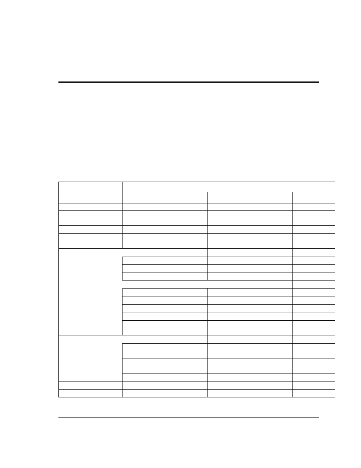
Table of Contents
Table of Contents
Table of ContentsTable of Contents
Chapter 1
ABOUT THIS MANUAL
1.1 AUDIENCE................................................................................................................. 1-1
1.2 MANUAL ORGANIZATION..................................................................................... 1-1
1.3 TERMINOLOGY AND CONVENTIONS ................................................................. 1-1
1.4 REFERENCES............................................................................................................. 1-3
Chapter 2
GENERAL DESCRIPTION
2.5 PRODUCT OVERVIEW ............................................................................................. 2-5
2.6 KEY FEATURES......................................................................................................... 2-5
2.7 Regulatory Compliance Standards.............................................................................. 2-7
2.8 HARDWARE REQUIREMENTS................................................................................ 2-7
Chapter 3
INSTALLATION
3.1 SPACE REQUIREMENTS.......................................................................................... 3-1
3.2 UNPACKING INSTRUCTIONS ................................................................................ 3-2
3.3 HARDWARE OPTIONS............................................................................................. 3-4
3.3.1 Cable Select (CS) Jumper .................................................................................. 3-5
3.3.2 Drive Select (DS) Jumper .................................................................................. 3-6
3.3.3 Master Jumper configuration ............................................................................. 3-6
3.3.4 Jumper Parking (PK) Position ........................................................................... 3-6
3.3.5 Alternate Capacity (AC) .................................................................................... 3-7
3.4 ATA BUS ADAPTER.................................................................................................. 3-8
3.4.1 40-Pin ATA Bus Connector ............................................................................... 3-8
3.4.2 Adapter Board .................................................................................................... 3-8
3.5 MOUNTING ............................................................................................................... 3-9
3.5.1 Orientation ......................................................................................................... 3-9
3.5.2 Clearance .......................................................................................................... 3-11
3.5.3 Ventilation ........................................................................................................ 3-11
3.6 COMBINATION CONNECTOR (J1) ...................................................................... 3-11
3.6.1 DC Power (J1, Section A) ................................................................................ 3-12
3.6.2 External Drive Activity LED ............................................................................ 3-12
3.6.3 ATA Bus Interface Connector (J1, Section C) ................................................ 3-12
3.7 FOR SYSTEMS WITH A MOTHERBOARD ATA ADAPTER............................... 3-13
3.8 FOR SYSTEMS WITH AN ATA ADAPTER BOARD............................................. 3-13
3.8.1 Adapter Board Installation ............................................................................... 3-13
3.9 TECHNIQUES IN DRIVE CONFIGURATION ...................................................... 3-15
3.9.1 The 528-Megabytes Barrier .............................................................................. 3-15
Quantum Fireball Plus AS 10.2/20.5/30.0/40.0/60.0 GB AT iii
Page 4

Table of Contents
3.9.2 The 8.4-Gigabytes Barrier .................................................................................3-16
3.9.3 Operating system limitations ............................................................................3-16
3.10 SYSTEM STARTUP AND OPERATION................................................................. 3-17
Chapter 4
SPECIFICATIONS
4.1 SPECIFICATION SUMMARY ................................................................................... 4-1
4.2 FORMATTED CAPACITY.......................................................................................... 4-3
4.3 DATA TRANSFER RATES......................................................................................... 4-3
4.4 TIMING SPECIFICATIONS ...................................................................................... 4-4
4.5 POWER........................................................................................................................ 4-5
4.5.1 Power Sequencing ..............................................................................................4-5
4.5.2 Power Reset Limits .............................................................................................4-5
4.5.3 Power Requirements ...........................................................................................4-6
4.6 ACOUSTICS................................................................................................................ 4-7
4.7 MECHANICAL ........................................................................................................... 4-8
4.8 ENVIRONMENTAL CONDITIONS.......................................................................... 4-8
4.9 SHOCK AND VIBRATION........................................................................................ 4-9
4.10 HANDLING the DRIVE ........................................................................................... 4-10
4.11 RELIABILITY............................................................................................................ 4-10
4.12 ELECTROMAGNETIC SUSCEPTIBILITY.............................................................. 4-11
4.13 SPINDLE IMBALANCE........................................................................................... 4-11
4.14 DISK ERRORS.......................................................................................................... 4-11
Chapter 5
BASIC PRINCIPLES OF OPERATION
5.1 Quantum Fireball Plus AS DRIVE MECHANISM..................................................... 5-1
5.1.1 Base Casting Assembly .......................................................................................5-3
5.1.2 DC Motor Assembly ...........................................................................................5-3
5.1.3 Disk Stack Assemblies ........................................................................................5-3
5.1.4 Headstack Assembly ...........................................................................................5-4
5.1.5 Rotary Positioner Assembly ................................................................................5-4
5.1.6 Automatic Actuator Lock ...................................................................................5-4
5.1.7 Air Filtration .......................................................................................................5-5
5.2 DRIVE ELECTRONICS.............................................................................................. 5-5
5.2.1 Integrated µProcessor, Disk Controller and ATA Interface Electronics ............5-6
5.2.2 Read/Write ASIC ................................................................................................5-8
5.2.3 PreAmplifier and Write Driver .........................................................................5-10
5.3 FIRMWARE FEATURES .......................................................................................... 5-10
5.3.1 Disk Caching .....................................................................................................5-10
5.3.2 Head and Cylinder Skewing .............................................................................5-12
5.3.3 Error Detection and Correction ........................................................................5-13
5.3.4 Defect Management ..........................................................................................5-15
iv Quantum Fireball Plus AS 10.2/20.5/30.0/40.0/60.0 GB AT
Page 5

Table of Contents
Chapter 6
ATA BUS INTERFACE AND ATA COMMANDS 6-1
6.1 INTRODUCTION....................................................................................................... 6-1
6.2 SOFTWARE INTERFACE.......................................................................................... 6-1
6.3 MECHANICAL DESCRIPTION................................................................................ 6-1
6.3.1 Drive Cable and Connector ................................................................................ 6-1
6.4 ELECTRICAL INTERFACE ....................................................................................... 6-1
6.4.1 ATA Bus Interface .............................................................................................. 6-1
6.4.2 Host Interface Timing ........................................................................................ 6-9
6.5 REGISTER ADDRESS DECODING ....................................................................... 6-21
6.6 REGISTER DESCRIPTIONS ................................................................................... 6-22
6.6.1 Control Block Registers .................................................................................... 6-22
6.6.2 Command Block Registers ............................................................................... 6-24
6.7 COMMAND DESCRIPTIONS................................................................................. 6-29
6.7.1 Recalibrate ........................................................................................................ 6-29
6.7.2 Read Sectors ..................................................................................................... 6-30
6.7.3 Write Sectors .................................................................................................... 6-31
6.7.4 Read Verify Sectors .......................................................................................... 6-32
6.7.5 Seek .................................................................................................................. 6-33
6.7.6 Execute Drive Diagnostics ............................................................................... 6-34
6.7.7 INITIALIZE DRIVE PARAMETERS .............................................................. 6-36
6.7.8 Download Microcode ....................................................................................... 6-37
6.7.9 SMART ............................................................................................................. 6-38
6.7.10 Read Multiple Sectors ...................................................................................... 6-48
6.7.11 Write Multiple Sectors ........................... ....................................... ...... ....... ...... 6-49
6.7.12 Set Multiple Mode ........................... ...... ...... ....... ...... ....... ...... ....... ...... ....... ...... 6-50
6.7.13 Read DMA ............................................. ...... ....... ...... ....... ...... ....... ...... ....... ...... 6-51
6.7.14 Write DMA ...... ....... ...... ....... ...... ....... ...... ...... ....... ...... ....... ...... .......................... 6-52
6.7.15 STANDBY IMMEDIATE ............................ ....... ...... ....... ...... ....... ...... ....... ...... 6-54
6.7.16 IDLE IMMEDIATE ......................................................... ...... ....... ...... ....... ...... 6-55
6.7.17 STANDBY ............................................. ...... ....... ...... ....................................... 6-56
6.7.18 IDLE .......... ...... ....... ...... ....... ...... ....... ...... ...... ....................................... ....... ...... 6-57
6.7.19 READ BUFFER ................... ...... ....... ...... ...... ....................................... ....... ...... 6-58
6.7.20 CHECK POWER MODE ................................................................................. 6-59
6.7.21 SLEEP .............................................. ...... ...... ....... ....................................... ...... 6-60
6.7.22 FLUSH CACHE ........................ ....... ...... ...... ....... ...... ....... ................................ 6-61
6.7.23 WRITE BUFFER .............................. ...... ...... ....... ...... ....... ...... ....... ...... ....... ...... 6-62
6.7.24 IDENTIFY DRIVE .................... ....... ...... ...... ....... ...... ....... ...... ....... ................... 6-63
6.7.25 Set Features EFh .............................................................................................. 6-71
6.7.26 Set Features (Ultra ATA/100) ......................................................................... 6-71
6.7.27 Read Defect List ............................................................................................... 6-72
6.7.28 Configuration ...................................................... ...... ....... ...... ....... ...... ....... ...... 6-75
6.7.29 Host Protected Mode Feature .......................................................................... 6-79
6.8 ERROR REPORTING............................................................................................... 6-86
Quantum Fireball Plus AS 10.2/20.5/30.0/40.0/60.0 GB AT v
Page 6

List of Figures
List of Figures
List of FiguresList of Figures
Figure 3-1 Mechanical Dimensions of Quantum Fireball Plus AS Hard Disk Drive ......3-1
Figure 3-2 Drive Packing Assembly .................................................................................3-2
Figure 3-3 Drive Packing Assembly of a Polypropylene 20-Pack Container ...................3-3
Figure 3-4 Jumper Locations for the Quantum Fireball Plus AS Hard Disk Drive ........3-4
Figure 3-5 Jumper Locations on the Interface Connector ...............................................3-4
Figure 3-6 AT Connector and Jumper Location ..............................................................3-7
Figure 3-7 Mounting Dimensions for the Quantum Fireball Plus AS
Hard Disk Drives ..................................... ....... ...... ....... ...... ....... ...... ....... ...... ...3-9
Figure 3-8 Mounting Screw Clearance for the Quantum Fireball Plus AS
Hard Disk Drives ..................................... ....... ...... ....... ...... ....... ...... ....... ...... .3-10
Figure 3-9 J1 DC Power and ATA Bus Combination Connector ......................................3-11
Figure 3-10 Drive Power Supply and ATA Bus Interface Cables ....................................3-14
Figure 3-11 Completing the Drive Installation ................................................................3-15
Figure 5-1 Quantum Fireball Plus AS AT Hard Disk Drive Exploded View ..................5-2
Figure 5-2 Quantum Fireball Plus AS AT Hard Disk Drive Block Diagram ...................5-5
Figure 5-3 Block Diagram ................................................................................................5-6
Figure 5-4 Sector Data Field with ECC Check Bytes ....................................................5-14
Figure 6-1 PIO Interface Timing ....................................................................................6-10
Figure 6-2 Multiword DMA Bus Interface Timing ........................................................6-11
Figure 6-3 Initiating a Data In Burst ..............................................................................6-15
Figure 6-4 Sustained Data In Burst ...............................................................................6-15
Figure 6-5 Host Pausing a Data In Burst .......................................................................6-16
Figure 6-6 Device Terminating a Data In Burst .............................................................6-16
Figure 6-7 Host Terminating a Data In Burst ................................................................6-17
Figure 6-8 Initiating a Data Out Burst ...........................................................................6-17
Figure 6-9 Sustained Data Out Burst ............................................................................6-18
Figure 6-10 Device Pausing a Data Out Burst .................................................................6-18
Figure 6-11 Host Terminating a Data Out Burst .............................................................6-19
Figure 6-12 Device Terminating a Data out Burst ...........................................................6-20
Figure 6-13 Host Interface RESET Timing ......................................................................6-20
Quantum Fireball Plus AS 10.2/20.5/30.0/40.0/60.0 GB AT vi
Page 7

List of Tables
List of Tables
List of TablesList of Tables
Table 3-1 AT Jumper Options................................................................................................. 3-5
Table 3-2 J1 Power Connector, Section A............................................................................ 3-12
Table 3-3 Logical Addressing Format................................................................................... 3-17
Table 4-1 Specifications.......................................................................................................... 4-1
Table 4-2 Formatted Capacity ................................................................................................ 4-3
Table 4-3 Timing Specifications ............................................................................................. 4-4
Table 4-4 Power Reset Limits................................................................................................. 4-5
Table 4-5 Typical Power and Current Consumption.............................................................. 4-6
Table 4-6 Acoustical Characteristics—Sound Power............................................................. 4-7
Table 4-7 Environmental Specifications............ ....... ...... ...... ....... ....................................... .... 4-8
Table 4-8 Shock and Vibration Specifications....................................................................... 4-9
Table 4-9 Error Rates............................................................................................................ 4-11
Table 5-1 Cylinder Contents................................................................................................... 5-3
Table 5-2 Skew Offsets ......................................................................................................... 5-13
Table 6-1 Drive Connector Pin Assignments (J1, Section C) ............................................... 6-2
Table 6-2 Series Termination for Ultra ATA/100 .................................................................. 6-6
Table 6-3 Signal Line Definitions........................................................................................... 6-8
Table 6-4 Interface Signal Name Assignments....................................................................... 6-8
Table 6-5 PIO Host Interface Timing................................................................................... 6-10
Table 6-6 Multiword DMA Host Interface Timing .............................................................. 6-11
Table 6-7 Ultra DMA Data Transfer Timing Requirements................................................. 6-12
Table 6-8 Ultra DMA Data Burst Timing Descriptions ....................................................... 6-13
Table 6-9 Host Interface RESET Timing.............................................................................. 6-20
Table 6-10 I/O Port Functions and Selection Addresses....................................................... 6-21
Table 6-11 Command Block Register Initial Values............................................................... 6-22
Table 6-12 Device Control Register Bits ................................................................................ 6-23
Table 6-13 Drive Address Register Bits.................................................................................. 6-24
Table 6-14 Error Register Bits ................................................................................................ 6-25
Table 6-15 Drive Head Register Bits ...................................................................................... 6-26
Table 6-16 Status Register Bits............................................................................................... 6-27
Table 6-17 Quantum Fireball Plus AS 10.2/20.5/30.0/40.0/60.0 GB AT
Command Codes and Parameters......................................................................... 6-28
Table 6-18 Diagnostics Codes................................................................................................. 6-34
Table 6-19 Device Attribute Thresholds Data Structure ...................................................... 6-43
Table 6-20 Individual Threshold Data Structure .................................................................. 6-43
Table 6-21 Device SMART Data Structure............................................................................ 6-44
Table 6-22 Valid Count Range................................................................................................ 6-56
Table 6-23 Sector Count Result Value and Status................................................................. 6-59
Table 6-24 Identify Drive Parameters..................................................................................... 6-65
Table 6-25 Transfer/Mode Values .......................................................................................... 6-71
Table 6-26 READ DEFECT LIST LENGTH Command Bytes .............................................. 6-72
Table 6-27 AT READ DEFECT LIST Command Bytes ......................................................... 6-73
Quantum Fireball Plus AS 10.2/20.5/30.0/40.0/60.0 GB AT vii
Page 8

Table of Contents
Table 6-28 DEFECT LIST DATA FORMAT.......................................................................... 6-74
Table 6-29 DEFECT ENTRY DATA FORMAT...................................................................... 6-74
Table 6-30 Accessing the READ CONFIGURATION Command.......................................... 6-75
Table 6-31 Accessing the SET CONFIGURATION Command ............................................. 6-76
Table 6-32 Accessing the SET CONFIGURATION WITHOUT
SAVING TO DISK Command.............................................................................. 6-77
Table 6-33 Configuration Command Format.......................................................................... 6-78
Table 6-34 Command Errors ................................................................................................... 6-86
viii Quantum Fireball Plus AS 10.2/20.5/30.0/40.0/60.0 GB AT
Page 9

This chapter gives an overview of the contents of this manual, including the
intended audience, how the manual is organiz ed, terminology and conventions, and
references.
1.1
1.1 AUDIENCE
1.11.1
1.2
1.2 MANUAL ORGANIZATION
1.21.2
AUDIENCE
AUDIENCEAUDIENCE
The Quantum Fireball Plus ASM™10.2/20.5/30.0/40.0/60.0 GB AT Product
Manual is intended for several audiences. These audiences include: the end user,
installer, developer, original equipment manufacturer (OEM), and distributor. The
manual provides information about installation, principles of operation, interface
command implementation, and maintenance.
MANUAL ORGANIZATION
MANUAL ORGANIZATIONMANUAL ORGANIZATION
This manual is org anized into the following chapters:
•Chapter 1 – About This Manual
Chapter 1
Chapter 1
Chapter 1Chapter 1
ABOUT THIS MANUAL
ABOUT THIS MANUAL
ABOUT THIS MANUALABOUT THIS MANUAL
•Chapter 2 – General Description
•Chapter 3 – Installation
•Chapter 4 – Specifications
•Chapter 5 – Basic Principles of Operation
•Chapter 6 – ATA Bus Interface and ATA Commands
1.3
1.3 TERMINOLOGY AND CONVENTIONS
1.31.3
TERMINOLOGY AND CONVENTIONS
TERMINOLOGY AND CONVENTIONSTERMINOLOGY AND CONVENTIONS
In the Glossary at the back of this manual, you can find definitions for many of the
terms used in this manual. In addition, the following abbreviations are used in this
manual:
• ASIC application-specific integrated circuit
• ATA advanced technology attachment
• bpi bits per inch
• dB decibels
• dBA decibels, A weighted
Quantum Fireball Plus AS 10.2/20.5/30.0/40.0/60.0 GB AT 1-1
Page 10

About This Manual
• ECC error correcting code
• fci flux changes per inch
•Hz hertz
•KB kilobytes
• LSB least significant bit
• mA milliamperes
• MB megabytes (1 MB = 1,000,000 bytes when referring to disk
storage and 1,048,576 bytes in all other cases)
• Mbit/s megabits per second
•MB/s megabytes per second
•MHz megahertz
•ms milliseconds
• MSB most significant bit
• mV millivolts
•ns nanoseconds
•tpi tracks per inch
•µs microseconds
•V volts
The typographical and naming conventions used in this manual are listed below.
Conventions that are unique to a specific table appear in the notes that follow that
table.
Typographical Conventions:
• Names of Bits: Bit names are presented in initial capitals. An example
is the Host Software Reset bit.
• Commands: Interface commands ar e listed in all capita ls. An example
is WRITE LONG.
• Register Names: Registers are g iven in this manual with initial
capitals. An example is the Alternate Status Register.
• Parameters: Pa rameter s are gi ven as init ial c apitals wh en spel led ou t,
and are given as all capi tals whe n a bbrevia te d. E xamples are Pref et ch
Enable (PE), and Cache Enable (CE).
• Hexadecimal Notation: The hexadecimal notation is given in 9-point
subscript form. An example is 30
.
H
• Signal Negation: A signal name that is defined as active low is listed
with a minus sign following the signal. An example is RD–.
• Messages: A message that is sent from the drive to the host is listed in
all capitals. An example is ILLEGAL COMMAND.
1-2 Quantum Fireball Plus AS 10.2/20.5/30.0/40.0/60.0 GB AT
Page 11

Naming Conventions:
• Host: I n general, the system in which the d rive reside s is refe rred to as
the host.
• Computer Voice: This refers to items you type at the computer
keyboard. These items are listed in 10-point, all capitals, Courier font.
An example is FORMAT C:/S.
1.4
1.4 REFERENCES
1.41.4
REFERENCES
REFERENCESREFERENCES
For additional information about the AT interface, refer to:
• IBM Technical Reference Manual #6183355, March 1986.
• ATA Common Access Method Specification, Revision 5.0.
About This Manual
Quantum Fireball Plus AS 10.2/20.5/30.0/40.0/60.0 GB AT 1-3
Page 12

About This Manual
1-4 Quantum Fireball Plus AS 10.2/20.5/30.0/40.0/60.0 GB AT
Page 13

This chapter summarizes the general functions and key features of the Quantum
Fireball Plus AS 10.2/20.5/30.0/40.0/60.0 GB AT hard disk drives, as well as the
applicable standards and regulations.
2.5
2.5 PRODUCT OVERVIEW
2.52.5
PRODUCT OVERVIEW
PRODUCT OVERVIEWPRODUCT OVERVIEW
Quantum’s Fireball Plus AS hard disk drives are part of a family of high
performance, 1-inch-high hard disk drives manufactured to meet the highest
product quality standards.
These hard disk drives use nonremovable, 3 1/2-inch hard disks and are
available with the ATA interface.
The Quantum Fireball Plus AS 10.2/20.5/30.0/40.0/60.0 GB AT hard disk drives
feature an embedded hard disk drive controller, and use ATA commands to
optimize system performance. Because the drive manages media defects and error
recovery internally, these operations are fully transparent to the user.
Chapter 2
Chapter 2
Chapter 2Chapter 2
GENERAL DESCRIPTION
GENERAL DESCRIPTION
GENERAL DESCRIPTIONGENERAL DESCRIPTION
The innovative design of the Quantum Fireball Plus AS hard disk drives
incorporate leading edge technologies such as Ultra ATA/100, Advanced Cache
Management, Shock Protection System™(SPS), Data Protection System (DPS )
and Quiet Drive Technology (QDT). Thes e enhanced techn ol ogi e s enab l e
Quantum to produce a family of high-p erformance, high-reliability drives.
2.6
2.6 KEY FEATURES
2.62.6
KEY FEATURES
KEY FEATURESKEY FEATURES
The Quantum Fireball Plus AS 10.2/20.5/30.0/40.0/60.0 GB AT hard disk drives
include the following key features:
General
• Formatted storage capacity of 10.2 GB (1 disk, 1 head), 20.5 GB (1 disk, 2
heads), 30.0 GB (2 disks, 3 heads), 40.0 GB (2 disks, 4 heads), and 60.0 GB
(3 disks, 6 heads)
• Low profile, 1-inch height
• Industry standard 3 1/2-inch form factor
• Emulation of IBM
commands
• Windows NT and 9X Certification
®
PC AT® task file register, and all AT fixed disk
Quantum Fireball Plus AS 10.2/20.5/30.0/40.0/60.0 GB AT 2-5
Page 14

General Description
Performance
• Average seek time of 8.5 ms
• Average rotational latency of 4.17 ms
• New Ultra ATA interface with Quantum-patented Ultra ATA/100 protocol
supporting burst data transfer rates of 100 MB/s.
• 2 MB buffer with 1.9 MB (approximate) Advance Cache Management
(ACM).
• Look-ahead DisCache feature with continuous prefetch and WriteCache
write-buffering capabilities
• AutoTask Register update, Multi-block AutoRead, and Multi-block
AutoWrite features in a custom ASIC
• Read-on-arrival firmware
• Quadruple-burst ECC, and double burst ECC on-the-fly
• 1:1 interleave on read/write operations
• Support of all standard ATA data transfer modes with PIO mode 4 and
multiword DMA mode 2, and Ultra DMA modes 0, 1, 2, 3, 4 and 5
• Adaptive cache segmentation
Reliability
• 625,000 hours mean time between failure (MTBF) in the field
• Automatic retry on read errors
• 344-bit, interleaved Reed-Solomon Error Correcting Code (ECC ), with cross
checking correction up to four separate bursts of 32 bits each totalling up to
128 bits in length
• S.M.A.R.T. 4 (Self-Monitoring, Analysis and Reporting Technology)
®
•Patented Airlock
automatic shipping lock, magnetic actuator retract, and
dedicated landing zone
• Transparent media defect mapping
• High performance, in-line defective sector skipping
• Reassignment of defective sectors discovered in the field, without
reformatting
• Shock Protection System to reduce handling induced failures
• Data Protection System to verify drive integrity
• Quiet Drive Technology (QDT)
Versatility
•Power saving modes
•Downloadable firmware
• Cable select feature
• Ability to daisy-chain two drives on the interface
2-6 Quantum Fireball Plus AS 10.2/20.5/30.0/40.0/60.0 GB AT
Page 15

2.7
2.7 Regulatory Compliance Standards
2.72.7
Regulatory Complianc e Standards
Regulatory Complianc e StandardsRegulatory Compliance Standards
Quantum Corporation’s disk drive products meet all domestic and international
product safety regulatory compliance requirements. Quantum’s disk drive products
conform to the following specifically marked Product Safety Standards:
• Underwriters Laboratories (UL) Standard 1950. This certificate is a
category certification pertaining to all 3.5-inch series drives models.
• Canadian Standards Association (CSA) Standard C.22.2 No. 1950.
This certificate is a category certification pertaining to all 3.5-inch
series drives models.
• TUV Rheinland Standard EN60 950. This certificate is a category
certification pertaining to all 3.5-inch series drives models.
Product EMI/EMS Qualifications:
Product EMI/EMS Qualifications:
Product EMI/EMS Qualifications:Product EMI/EMS Qu alifications:
• CE Mark authorization is granted by TUV Rheinland in compliance
with our qualifying under EN 55022:1994 and EN 50082-1:1997.
• C-Tick Mark is an Australian authorization marked noted on
Quantum’s disk drive products. The mark proves con formity to the
regulatory compliance document AS/NZS 3548: 1995 and BS EN
55022: 1995.
• Quantum’s disk drives are designed as a separate subas sembly that conforms
to the FCC Rules for Radiated and Conducted emissions, Part 15 Subpart J;
Class B when installed in a given computer system.
• Approval from Taiwan BSMI. Number: 3892A638
General Description
2.8
2.8 HARDWARE REQUIREMENTS
2.82.8
HARDWARE REQUIREMENTS
HARDWARE REQUIREMENTSHARDWARE REQUIREMENTS
The Quantum Fireball Plus AS hard disk drives are compatible with the IBM PC
AT, and other computers that are compatible with the IBM PC AT. It connects to
the PC either by means of a third-part y IDE-compatible adapter board, or b y
plugging a cable from the drive directly into a PC motherboard that supplies an
ATA interface.
Quantum Fireball Plus AS 10.2/20.5/30.0/40.0/60.0 GB AT 2-7
Page 16

General Description
2-8 Quantum Fireball Plus AS 10.2/20.5/30.0/40.0/60.0 GB AT
Page 17
This chapter explains how to unpack, configure, mount, and connect the Quantum
Fireball Plus AS 10.2/20.5/30.0/40.0/60.0 GB AT hard disk drive prior to
operation. It also explains how to start up and operate the drive.
3.1
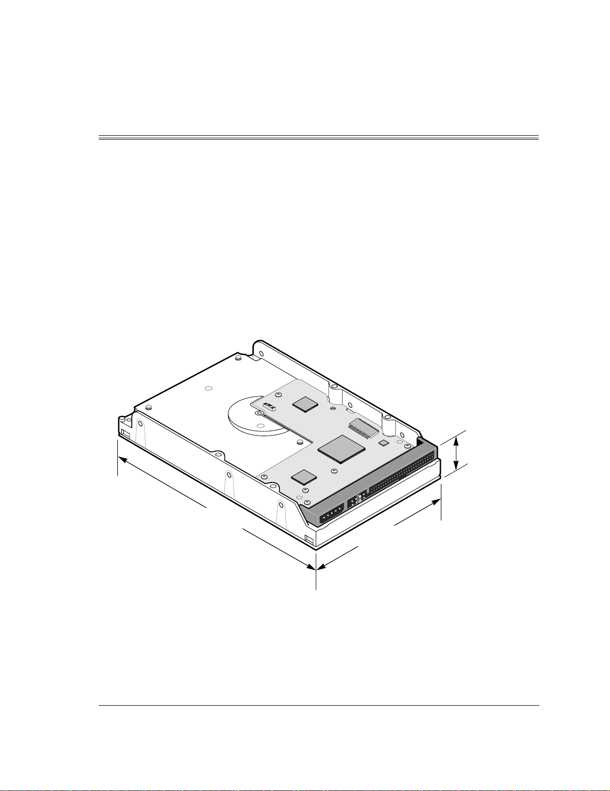
3.1 SPACE REQUIREMENTS
3.13.1
SPACE REQUIREMENTS
SPACE REQUIREMENTSSPACE REQUIREMENTS
The Quantum Fireball Plus AS hard disk drives are shipped without a faceplate.
Figure 3-1 shows the external dimensions of the Quantum Fireball Plus AS 10.2/
20.5/30.0/40.0/60.0 GB AT drives.
Chapter 3
Chapter 3
Chapter 3Chapter 3
INSTALLATION
INSTALLATION
INSTALLATIONINSTALLATION
Figure 3-1
Figure 3-1
Figure 3-1 Figure 3-1
26.1 mm (max)
(1.00 inches)
147 mm (max)
(5.75 inches)
101.6 ± 0.25 mm
(4.00 inches)
Mechanical Dimensions of Quantum Fireball Plus AS Hard Disk Drive
Quantum Fireball Plus AS 10.2/20.5/30.0/40.0/60.0 GB AT 3-1
Page 18
Installation
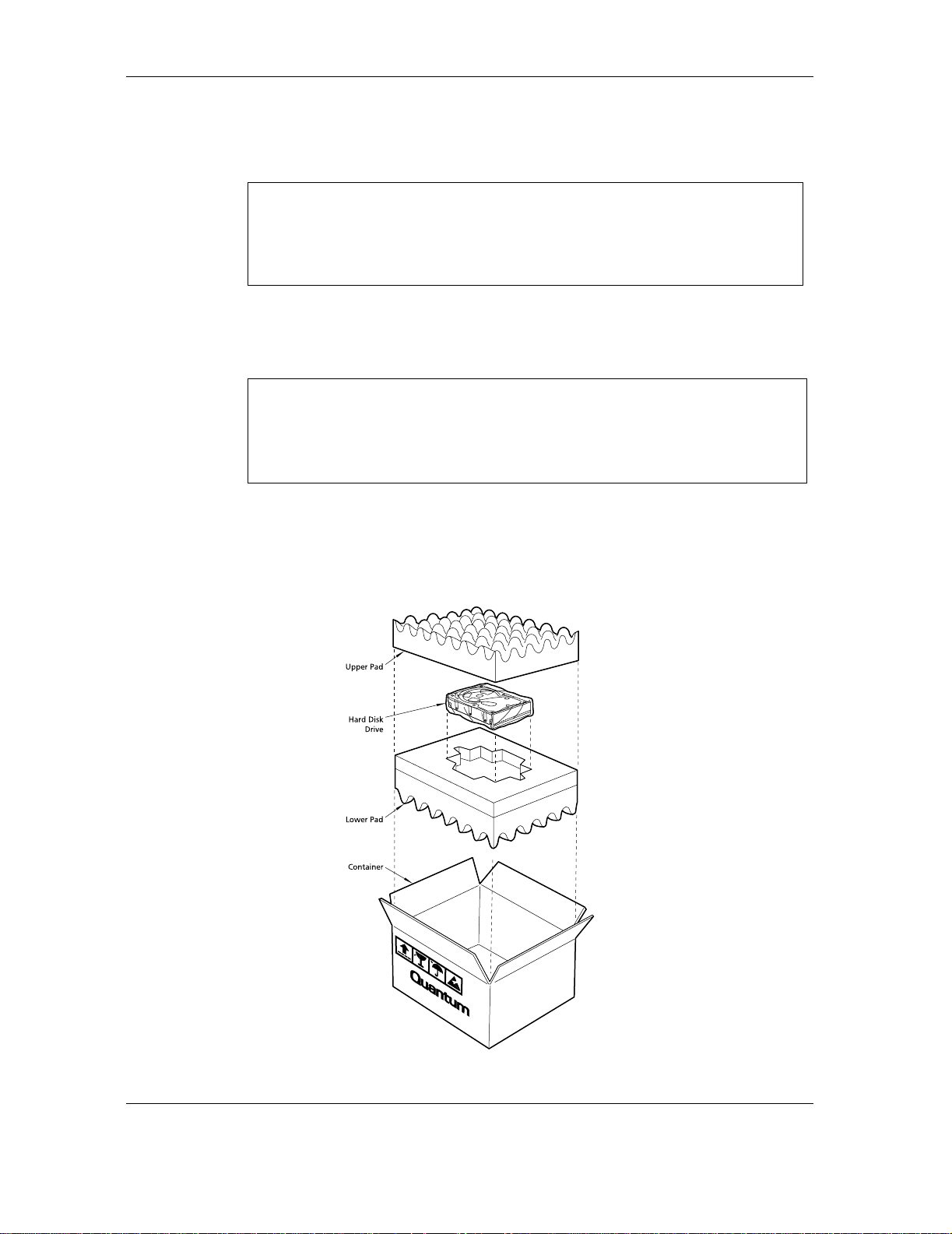
3.2
3.2 UNPACKING INSTRUCTIONS
3.23.2
UNPACKING INSTRUCTIONS
UNPACKING INSTRUCTIONS UNPACKING INSTRUCTIONS
CAUTION:
CAUTION: The maximum limits for phys ical shock can be exceeded if the
CAUTION:CAUTION:
1. Open the shipping container and remove the packing assembly that
contains the drive.
2. Remove the driv e from th e packing assembly.
CAUTION:
CAUTION: During shipment and handling, the antistatic electrostatic dis-
CAUTION:CAUTION:
3. When you are ready to install the drive, remove it from the ESD bag.
drive is not handled properly. Special care should be
taken not to bump or drop the drive. It is highly recommended
that Quantum Fireball Plus AS drives are not stacked or placed
on any hard surface after they ar e unpacked. Such handling
could cause media damage.
charge (ESD) bag prevents electronic component
damage due to electrostati c discharge. To av oid accidental damage to the drive, do not use a sharp instrume nt to open the ESD
bag and do not touch PCB components. Save the packing materials for possible future use.
Figure 3-2 shows the packing assembly for a single Quantum Fireball Plus AS
hard disk drive. A 20-pack shipping container is available for multiple drive
shipments.
Figure 3-2
Figure 3-2
Figure 3-2 Figure 3-2
3-2 Quantum Fireball Plus AS 10.2/20.5/30.0/40.0/60.0 GB AT
Drive Packing Assembly
Page 19
Installation
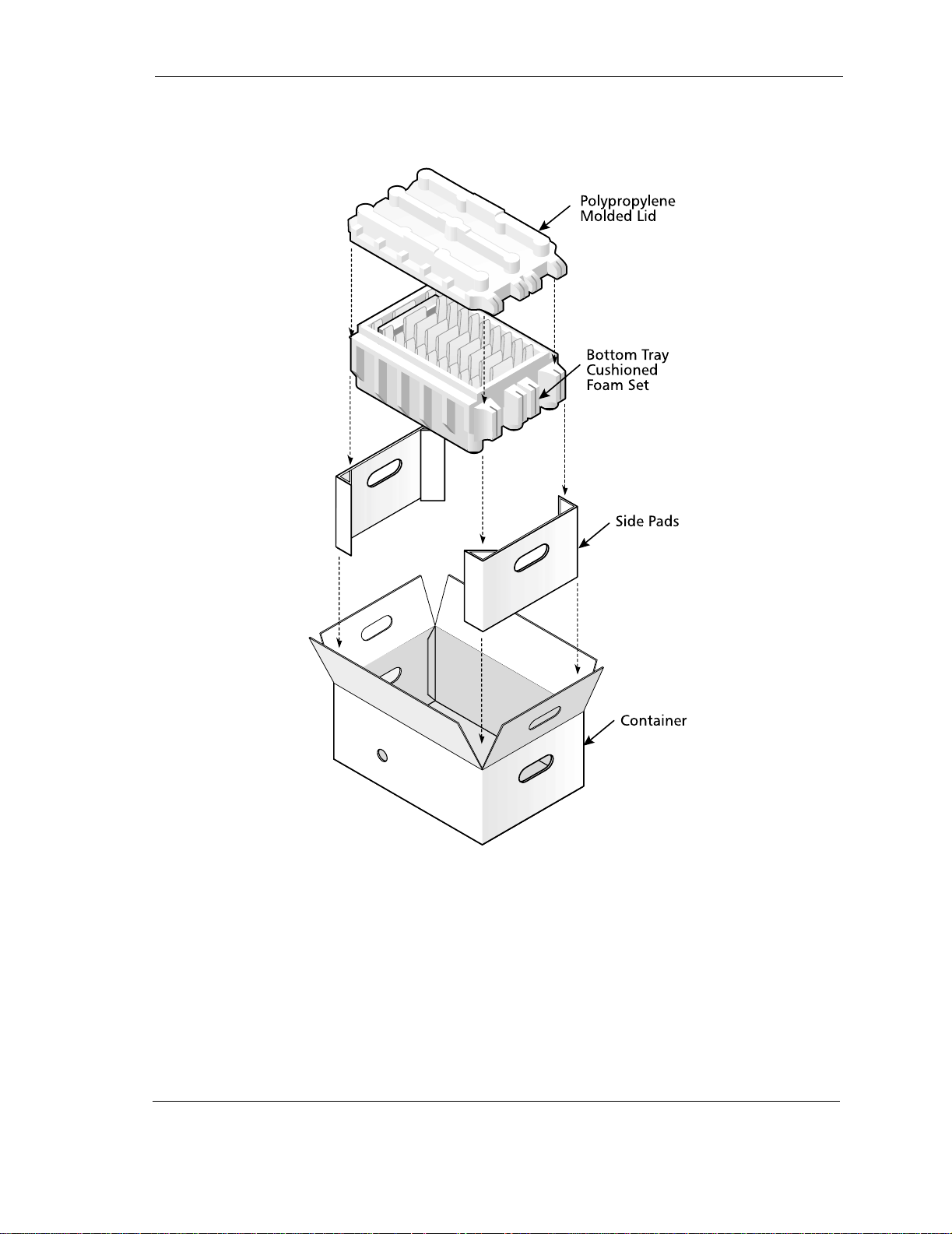
Figure 3-3
Figure 3-3 Drive Packing Assembly of a Polypropylene 20-Pack Container
Figure 3-3 Figure 3-3
Note: The 20-pack container should be shipped in the same way it
was received from Quantum. When individual drives are
shipped from the 20-pack container then it should be appropriately packaged (n ot supplied wi th the 20-pack) to prevent damage.
Quantum Fireball Plus AS 10.2/20.5/30.0/40.0/60.0 GB AT 3-3
Page 20
Installation
3.3
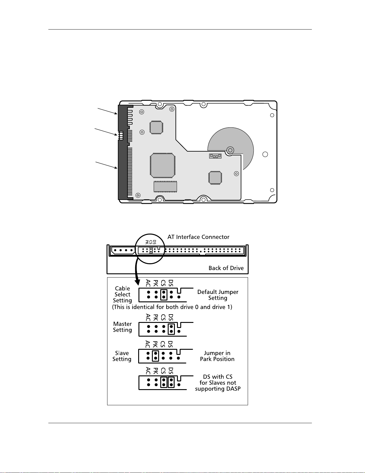
3.3 HARDWARE OPTIONS
3.33.3
HARDWARE OPTIONS
HARDWARE OPTIONSHARDWARE OPTIONS
The configuration of a Quantum Fireball Plus AS 10.2/20.5/30.0/40.0/60.0 GB
AT hard disk dr iv e d ep end s on th e h os t syst em in wh i ch i t is t o be ins ta ll ed. T hi s
section describes the hardware options that you must take into account prior to
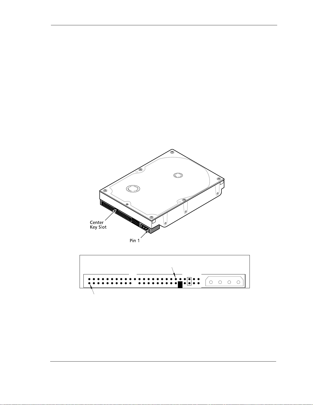
installation. Figure 3-4 shows the printed circuit board (PCB) assembly,
indicating the jumpers that control some of these options.
DC Power
Connector
Jumpers
ATA-Bus
Interface
Header
Figure 3-4
Figure 3-4
Figure 3-4 Figure 3-4
Back of
Drive
Front
Drive
Jumper Locations for the Quantum Fireball Plus AS Hard Disk Drive
Figure 3-5
Figure 3-5 Jumper Locations on the Interface Connector
Figure 3-5 Figure 3-5
3-4 Quantum Fireball Plus AS 10.2/20.5/30.0/40.0/60.0 GB AT
Page 21
CS
CS DS
CSCS
DS PK
DSDS
Installation
The configuration of the following Three jumpers controls the drive’s five modes
of operation:
•CS – Cable Select
• DS – Drive Select
•PK– Jumper Parking Position (Slave mode)
• AC– Alternate Capacity
The AT PCB has two jumper locatio ns provided to configure t he drive in a system.
The default configuration for the drive as shipped from the factory is with a
jumper across the DS location, and open positions in the CS, PK and AC
positions.
Table 3-1 defines the operation of the master/slave jumpers and their function
relative to pin 28 on the interface. 1 indicates that the specified jumper is installed;
0 indicates that the jumper is not installed.
Table 3-1
Table 3-1
Table 3-1 Table 3-1
PK PIN 28
PKPK
PIN 28 DESCRIPTION
PIN 28PIN 28
AT Jumper Options
DESCRIPTION
DESCRIPTIONDESCRIPTION
0 0 X X Drive is configured as a slave
1 0 X Gnd Drive is configured as Master (Device 0) when attached
to the end of a 80 conductor Ultra ATA cable
0 1 X X Drive is configured as a Master
1 0 X Open Drive is configured as a Slave (Device 1) when attached
to the middle of a 80 conductor Ultra ATA cable
1 1 X X Drive is configured as a Master with an attached slave
that does not support DASP
Note: In Table 3-1, a 0 indicates that the jumper is removed, a 1 indi-
3.3.1
3.3.1 Cable Select (CS) Jumper
3.3.13.3.1
Cable Select (CS) Jumper
Cable Select (CS) JumperCable Select (CS) Jumper
When a Quantum Fireball Plus AS 10.2/20.5/30.0/40.0/60.0 GB AT hard disk
drive and another ATA hard disk drive are daisy-chained together, they can be
configured as Master or Slave either by the CS or DS jumpers. To configure the
drive as a Master or Slav e with the CS feature, the CS jumper is in stalled (1). Th e
drive's position on the 80 conductor Ultra ATA data cable then determines
whether the drive is a Master (Device 0) or a Slave (Device 1). If the drive is
connected to the end of the Ultra (cable Select) data cable the drive is a Master.
If the drive is connected to the middle connection it is set as a Slave.
cates that the jumper is installed, and an X indicates that the
jumper setting does not matter.
Once you install the C S jumper, the driv e is configured as a Ma ster or Slave by t he
state of the Cable Sele ct signal: pin 28 of the ATA bus conne ctor. Please no te that
pin 28 is a vendor-specific pin that Quantum is using for a specific purpose. More
than one function is allocated to CS, according to the ATA CAM specification
(see reference to this specification in Chapter 1). If pin 28 is a 0 (grounded), the
Quantum Fireball Plus AS 10.2/20.5/30.0/40.0/60.0 GB AT 3-5
Page 22

Installation
drive is configured as a Master. If it is a 1 (high), the drive is configured as a Slave.
In order to configure two drives in a Master/Slave relationship using the CS
jumper, you need to use a cable that provides the proper signal level at pin 28 of
the ATA bus connector. This allows two drives to operate in a Master/Slave
relationship according to the drive cable placement.
The Quantum Fireball Plus AS 10.2/20.5/30.0/40.0/60.0 GB AT hard disk drives
are shipped from the f actory as a Master (Device 0 - CS jumper installed). To
configure a drive as a Slave (Device 1- DS scheme), the CS jumper must be
removed. In this configuration, the spare jumper removed from the CS position
may be stored on the PK jumper pins.
3.3.2
3.3.2 Drive Select (DS) Jumper
3.3.23.3.2
3.3.3
3.3.3 Master Jumper configuration
3.3.33.3.3
Drive Select (DS) Jumper
Drive Select (DS) JumperDrive Select (DS) Jumper
You can also daisy-chain two drives on the ATA bus interface by using their Drive
Select (DS) jumper s. To use th e DS fea ture, th e CS ju mper must not be inst alled .
To configure a drive as the Master (Device 0), a jumper must be installed on the
DS pins.
Note: The order in which drives are connected in a daisy chain has no
significance.
Master Jumper configuration
Master Jumper configurationMaster Jumper configuration
In combination with the current DS or CS jumper s ettings, the Slave Present (SP)
jumper can be implemented if necessary as follows:
Note: The CS position doubles as the Slave present on this drive.
• When the drive is configured a s a Master
jumper installed, and the Cable Select signal is set to (0), adding an
additional jumper (both jumpers DS and CS now installed) will
indicate to the drive that a Slave drive is present. This Master with
Slave Present jumper configuration shoul d be instal led on the Master
drive only if the Slave drive does not use the Drive Active/Slave
Present (DASP–) signal to indicate its presence.
3.3.4
3.3.4 Jumper Parking (PK) Position
3.3.43.3.4
Jumper Parking (PK) Position
Jumper Parking (PK) PositionJumper Parking (PK) Position
The PK position is used as a holding place for the jumper for a slave drive in
systems that do not su pport Cable Select. The pins used for the parking positio n
are vendor unique.
(DS jumper install ed or CS
3-6 Quantum Fireball Plus AS 10.2/20.5/30.0/40.0/60.0 GB AT
Page 23
3.3.5
3.3.5 Alternate Capacity (AC)
3.3.53.3.5
10 GB
10 GB
10 GB10 GB
20 GB
20 GB
20 GB20 GB
40 GB
40 GB
40 GB40 GB
60 GB
60 GB
60 GB60 GB
Alternate Capacity (AC)
Alternate Capacity (AC)Alternate Capacity (AC)
For user capacities below 66,055,248 sectors (32 GB), inserting the AC jumper
limits the Number of Cylinders field 1 to a value of 16,383, as reported in
IDENTIFY DEVICE data word. This allows software drivers to determine that the
actual capacity is larger than indicated by the maximum CHS, requiring LBA
addressing to use the full capacity.
A summary of these effects for the Quantum Fireball Plus AS drives is shown in
the following table:
AC JUMPER OUT
AC JUMPER OUT AC JUMPER IN
AC JUMPER OUTAC JUMPER OUT
C=16,383
H=16
S=63
LBA=20,075,548
C=16,383
H=16
S=63
LBA=40,157,056
C=16,383
H=16
S=63
LBA=80,315,072
C=16,383
H=16
S=63
LBA=120,478,088
AC JUMPER IN
AC JUMPER INAC JUMPER IN
C=16,383
H=15
S=63
LBA=20,075,548
C=16,383
H=15
S=63
LBA=40,157,056
C=16,383
H=16
S=63
LBA=66,055,248
C=16,383
H=16
S=63
LBA= 66,055,248
Installation
Figure 3-6
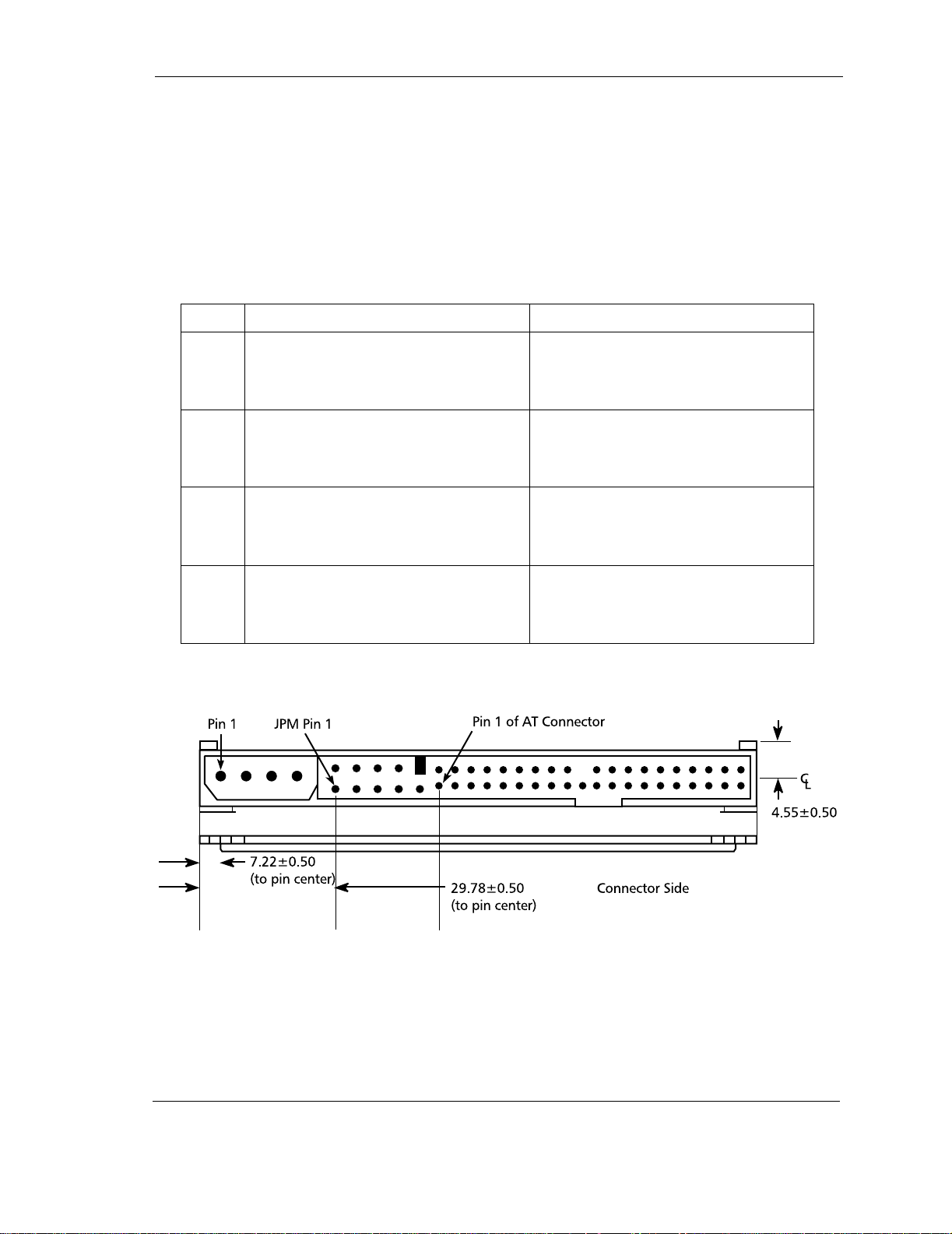
Figure 3-6
Figure 3-6 Figure 3-6
Quantum Fireball Plus AS 10.2/20.5/30.0/40.0/60.0 GB AT 3-7
AT Connector and Jumper Location
Page 24

Installation
3.4
3.4 ATA BUS ADAPTER
3.43.4
3.4.1
3.4.1 40-Pin ATA Bu s Connector
3.4.13.4.1
3.4.2
3.4.2 Adapter Board
3.4.23.4.2
ATA BUS ADAPTER
ATA BUS ADAPTERATA BUS ADAPTER
There are two ways you can configure a system to allow the Quantum Fireball Plus
AS hard disk drives to communicate over the ATA bus of an IBM or IBMcompatible PC:
1. Connect the drive to a 40-pin ATA bus connector (if available) on the
motherboard of the PC.
2. Install an IDE-compatible adapter board in the PC, and connect the drive
to the adapter board.
40-Pin ATA Bus Connector
40-Pin ATA Bus Connector40-Pin ATA Bus Connector
Most PC motherboards have a built-in 40-pin ATA bus connector that is
compatible with the 40-pin ATA interface of the Quantum Fireball Plus AS 10.2/
20.5/30.0/40.0/60.0 GB AT hard disk drives. If the motherboard has an ATA
connector, simply connect a 40-pin ribbon cable between the drive and the
motherboard.
You should also refer to the moth erboard instruction manual, and refer to Chapt er
6 of this manual to ensure signal compatibility.
Adapter Board
Adapter BoardAdapter Board
If your PC motherboard does not contain a built-in 40-pin ATA bus interface
connector, you must install an ATA bus adapter board and connecting cable to
allow the drive t o interface with the mo therboard. Quantum does not supply such
an adapter board, but they are available from several third-party vendors.
Please carefully read the instruction manual that comes with your adapter board,
as well as Chapter 6 of this manual to ensure signal compatibility between the
adapter board and the drive. Also, make sure that the adapter board jumper
settings are appropriate.
3-8 Quantum Fireball Plus AS 10.2/20.5/30.0/40.0/60.0 GB AT
Page 25
3.5
3.5 MOUNTING
3.53.5
3.5.1
3.5.1 Orientation
3.5.13.5.1
MOUNTING
MOUNTINGMOUNTING
Drive mounting orientation, clearance, and ventilation requirements are
described in the following subsections.
Orientation
OrientationOrientation
The mounting holes on the Quantum Fireball Plus AS 10.2/20.5/30.0/40.0/60.0
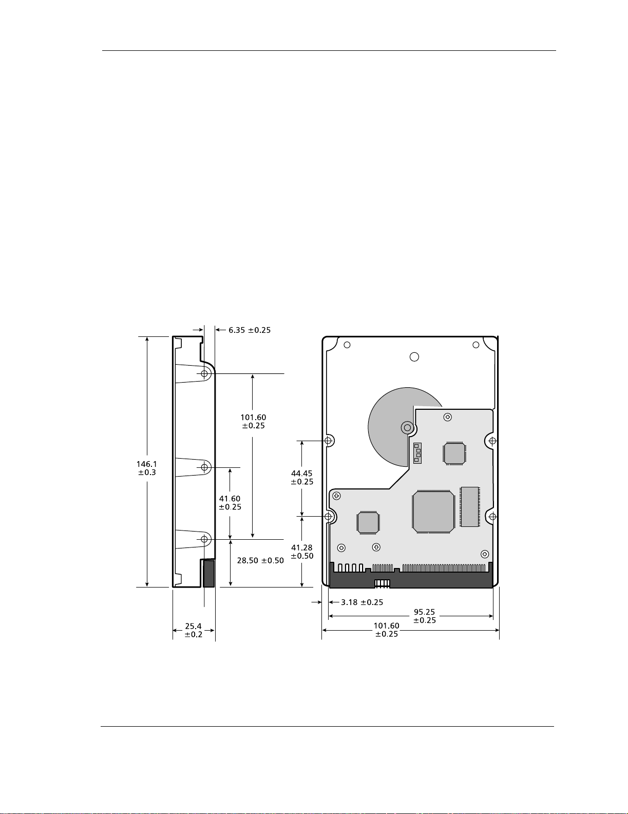
GB AT hard disk drives allow the drive to be mounted in any orientation. Figure
3-6 and Figure 3-7 show the location of the three mounting holes on each side of
the drive. The drive can also be mounted using the four mounting hole locations
on the PCB side of the drive.
Note: It is highly recommended that the drive is hard mounted on to
the chassis of the system being used for general operation, as
well as for test purposes. Failure to hard mount the drive can
result in erroneous errors during testing.
Drives can be mounted in any orientation. Normal position is
All dimensions are in millimeters. For mounting, #6-32 UNC screws are
recommended.
with the PCB facing down.
Installation
Figure 3-7
Figure 3-7
Figure 3-7 Figure 3-7
Mounting Dimensions for the Quantum Fireball Plus AS Ha rd Disk Drives
Quantum Fireball Plus AS 10.2/20.5/30.0/40.0/60.0 GB AT 3-9
Page 26
Installation
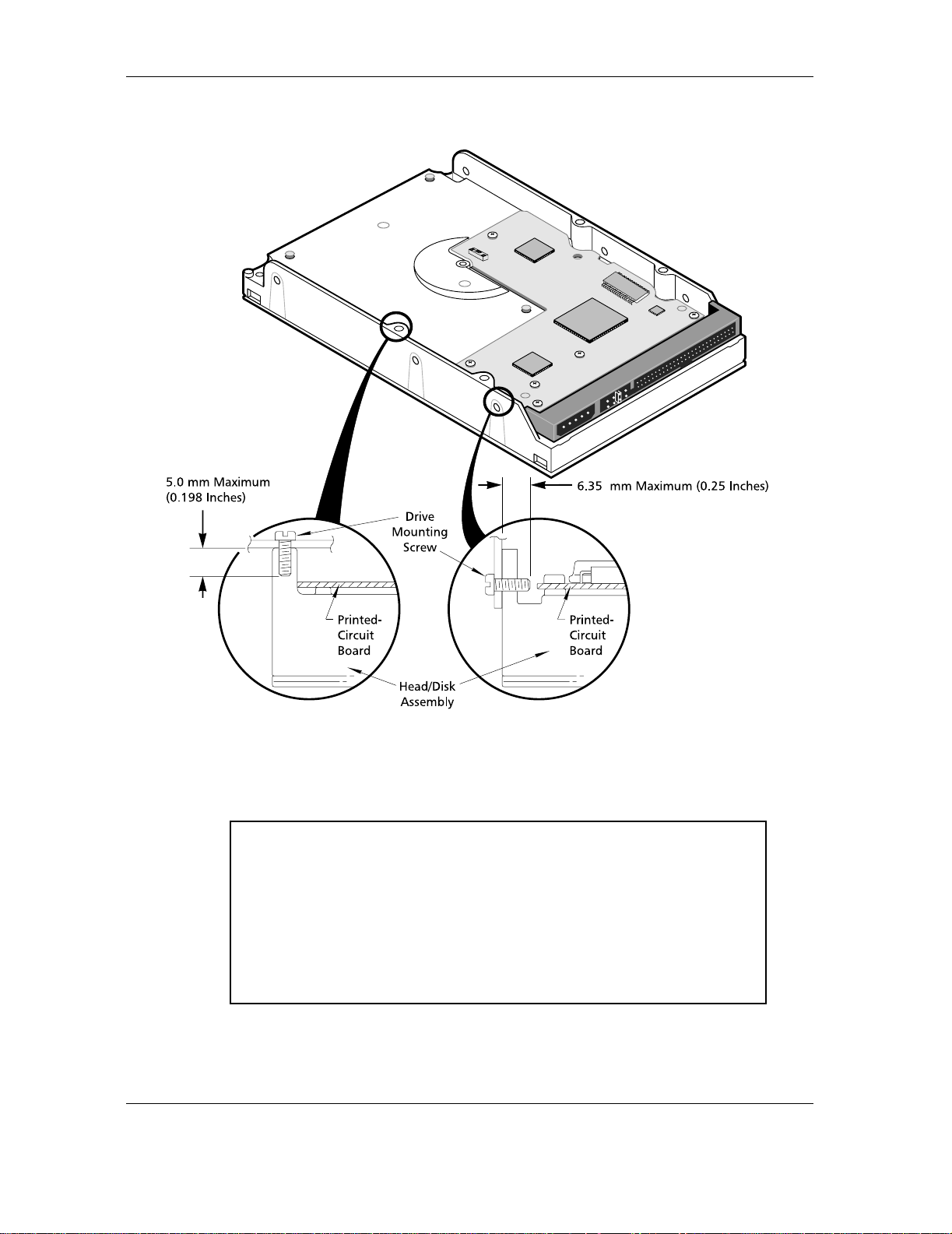
Figure 3-8
Figure 3-8 Mounting Screw Clearance for the Quantum Fireball Plus AS Hard Disk Drives
Figure 3-8 Figure 3-8
CAUTION:
CAUTION: The PCB is very close to the mounting holes. Do not ex-
CAUTION:CAUTION:
ceed the specified length for the mounting screws. The
specified screw length allows full use of the mounting
hole threads, while avoiding damaging or placing unwanted stress on the PCB. Figure 3-8 specifies the minimum clearance between the PCB and the screws in the
mounting holes. To avoid stripping the mounting hole
threads, the maximum torque applied to the screws must
not exceed 8 inch-pounds. A maximum screw length of
0.25 inches may be used.
3-10 Quantum Fireball Plus AS 10.2/20.5/30.0/40.0/60.0 GB AT
Page 27
3.5.2
3.5.2 Clearance
3.5.23.5.2
3.5.3
3.5.3 Ventilation
3.5.33.5.3
3.6
3.6 COMBINATION CONNECTOR (J1)
3.63.6
Clearance
ClearanceClearance
Clearance from the drive to any other surface (excep t mounting surfaces) must be
a minimum of 1.25 mm (0.05 inches).
Ventilation
VentilationVentilation
The Quantum Fireball Plus AS 10.2/20.5/30.0/40.0/60.0 GB AT hard disk drives
operate without a cooling fan, provided the ambient air temperature does not
exceed 131°F (55°C) at any point along the drive form factor envelope.
COMBINATION CONNECTOR (J1)
COMBINATION CONNECTOR (J1)COMBINATION CONNECTOR (J1)
J1 is a three-in-one combination connector. The drive’s DC power can be applied
to section A. The ATA bus interface (40-pin) uses section C. The connector is
mounted on the back edge of the printed-circuit board (PCB), as shown in Figure
3-9.
Installation
Pin 40
Figure 3-9
Figure 3-9
Figure 3-9 Figure 3-9
J1 IDE (40-Pin)/DC (4-Pin)
Combination Connector
40-Pin IDE
(J1 Section C)
Pin 1
4-Pin DC Power
(J1 Section A)
4321
J1 DC Power and ATA Bus Combination Connector
Quantum Fireball Plus AS 10.2/20.5/30.0/40.0/60.0 GB AT 3-11
Page 28
Installation
3.6.1
3.6.1 DC Power (J1, Section A)
3.6.13.6.1
NUMBER
NUMBER
NUMBERNUMBER
J1 Section A (4-Pin):
DC Power (J1, Section A)
DC Power (J1, Section A)DC Power (J1, Section A)
The recommended mating conne ctors for the +5 VDC and +12 VDC input power
are listed in Table 3-2.
Table 3-2
Table 3-2
Table 3-2 Table 3-2
PIN
PIN
PINPIN
1 +12 VDC 4-Pin Connector:
2 Ground
3 Ground
VOLTAGE
VOLTAGE
VOLTAGEVOLTAGE
LEVEL
LEVEL
LEVELLEVEL
Return for
+12 VDC
Return for
+5 VDC
J1 Power Connector, Section A
MATING CONNECTOR TYPE AND PART NUMBER
MATING CONNECTOR TYPE AND PART NUMBER
MATING CONNECTOR TYPE AND PART NUMBERMATING CONNECTOR TYPE AND PART NUMBER
AMP P/N 1-480424-0
Loose piece contacts:
AMP P/N VS 60619-4
Strip contacts:
AMP P/N VS 61117-4
(OR EQUIVALENT)
(OR EQUIVALENT)
(OR EQUIVALENT)(OR EQUIVALENT)
4+5 VDC
Note: Labels indicate the pin numbers on the connector. Pins 2 and 3 of
section A are the +5 and +12 volt returns and are connected together on the drive.
3.6.2
3.6.2 External Drive Activity LED
3.6.23.6.2
3.6.3
3.6.3 ATA Bus Interface Connector (J1, Section C)
3.6.33.6.3
External Drive Activity LED
External Drive Activity LED External Drive Activity LED
An external drive activity LED may be connected to the DASP-I/O pin 39 on J1.
For more details, see the pin description in Table 6-1.
ATA Bus Interface Connector (J1, Section C)
ATA Bus Interface Connector (J1, Section C)ATA Bus Interface Connector (J1, Section C)
On the Quantum Fireball Plus AS 10.2/20.5/30.0/40.0/60.0 GB AT hard disk
drives, the ATA bus interface cable c onnector (J1, section C) is a 40-pin Uni versal
Header, as shown in Figure 3-9.
To prevent the possibility of incorrect installation, the connector h as been keyed
by removing Pin 20. This ensures that a connector cannot be installed upside
down.
See Chapter 6, “ATA Bus Interface and ATA Commands,” for more detailed
information about the required signals. Refer to Table 6-1 for the pin assignments
of the ATA bus connector (J1, section C).
3-12 Quantum Fireball Plus AS 10.2/20.5/30.0/40.0/60.0 GB AT
Page 29

3.7
3.7 FOR SYSTEMS WITH A MOTHERBOARD ATA ADAPTER
3.73.7
3.8
3.8 FOR SYSTEMS WITH AN ATA ADAPTER BOARD
3.83.8
3.8.1
3.8.1 Adapter Board Installation
3.8.13.8.1
FOR SYSTEMS WITH A MOTHERBOARD ATA ADAPTER
FOR SYSTEMS WITH A MOTHERBOARD ATA ADAPTERFOR SYSTEMS WITH A MOTHERBOARD ATA ADAPTER
You can install the Quantum Fireball Plus AS 10.2/20.5/30.0/40.0/60.0 GB AT
hard disk drives in an AT-compatible system that contains a 40-pin ATA bus
connector on the motherboard.
To connect the drive to the motherboard, use a 40 conductor ribbon cable (80
conductor ribbo n cable if using Ultra ATA/100 drive) 18 inches in length or
shorter. Ensure that pin 1 of the drive is connected to pin 1 of the motherboard
connector.
FOR SYSTEMS WITH AN ATA ADAPTER BOARD
FOR SYSTEMS WITH AN ATA ADAPTER BOARDFOR SYSTEMS WITH AN ATA ADAPTER BOARD
To install the Quantum Fireball Plus AS 10.2/20.5/30.0/40.0/60.0 GB AT hard
disk drive in an AT-compatible system without a 40-pin ATA bus connector on its
motherboard, you need a third-party IDE-compatible adapter board.
Adapter Board Installation
Adapter Board InstallationAdapter Board Installation
Carefully read the manual that accompanies your adapter board before installing
it. Make sure that all the jumpers are set p roperly and th at there are no add ress or
signal conflicts. You must also investigate to see if your AT-compatible system
contains a combination floppy and hard disk controller board. If it does, you must
disable the hard disk drive controller functions on that controller board before
proceeding.
Installation
Once you have disabled the hard disk drive controller functions on the floppy/
hard drive controller, install the adapter board. Again, make sure that you have
set all jumper straps on the adapter board to avoid addressing and signal conflicts.
Note: For Sections 3.7 and 3.8, power should be turned off on the
computer before installing the drive.
Quantum Fireball Plus AS 10.2/20.5/30.0/40.0/60.0 GB AT 3-13
Page 30
Installation
3.8.1.1
3.8.1.1 Connecting the Adapter Boa rd and the Drive
3.8.1.13.8.1.1
Connecting the Adapter Board and the Drive
Connecting the Adapter Board and the DriveConnecting the Adapter Board and the Drive
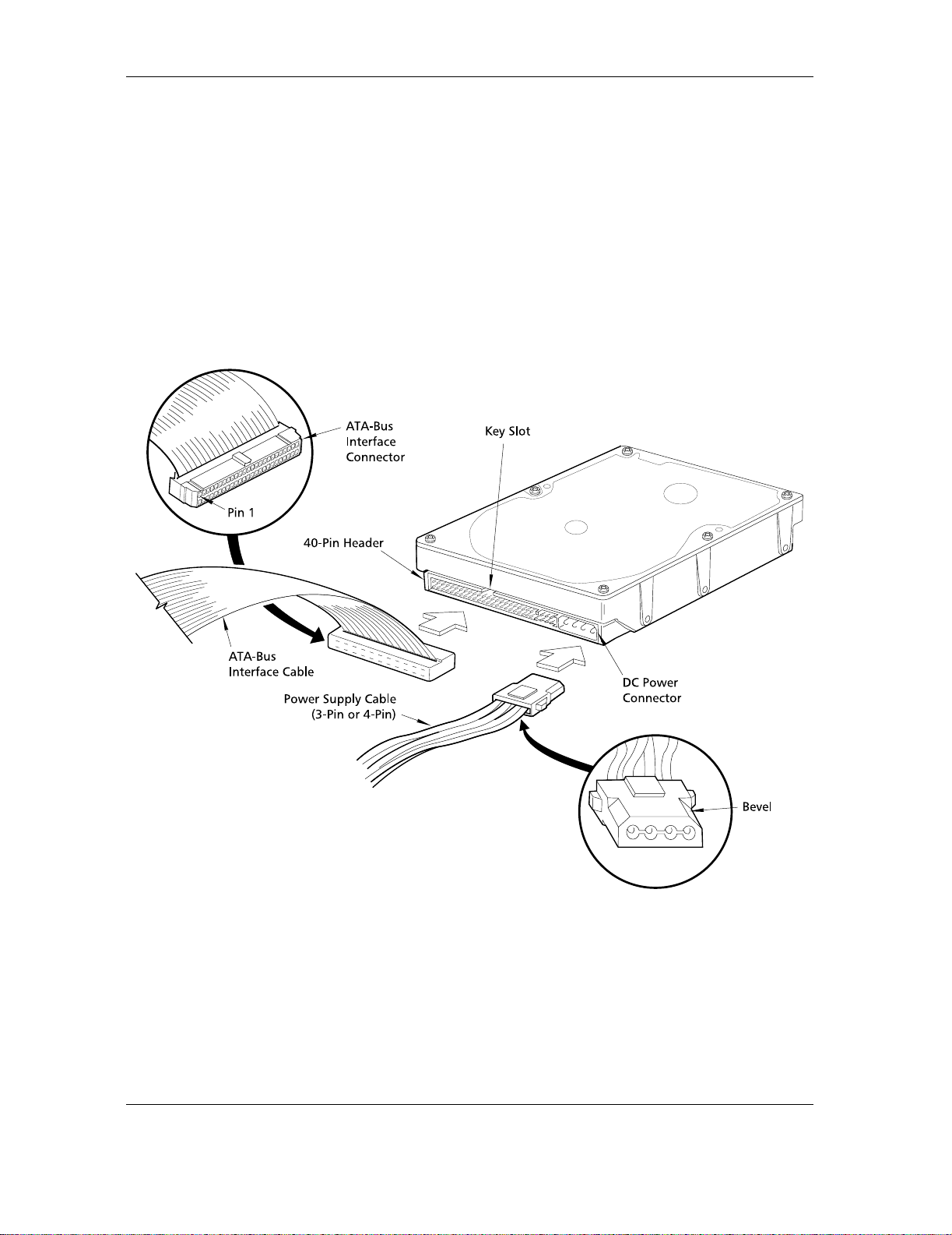
Use a 40-pin ribbon cable to connect the drive to the board. See Figure 3-10. To
connect the drive to the board:
1. Insert the 40-pin cable connector into the mating connector of the adapter
board. Make sure that pin 1 of th e connect or matches with pi n 1 on the cabl e.
2. Insert the other end of the cable into the header on the drive. When
inserting t his end of th e cable , make s ure th at pin 1 of th e cable connec ts
to pin 1 of the drive connector.
3. Secure the drive to the system chassis by using the mounting screws, as
shown in Figure 3-11.
Figure 3-10
Figure 3-10
Figure 3-10 Figure 3-10
Drive Power Supply and ATA Bus Interface Cables
3-14 Quantum Fireball Plus AS 10.2/20.5/30.0/40.0/60.0 GB AT
Page 31

Installation
Figure 3-11
Figure 3-11 Completing the Drive Installation
Figure 3-11 Figure 3-1 1
3.9
3.9 TECHNIQUES IN DRIVE CONFIGURATION
3.93.9
3.9.1
3.9.1 The 528-Megabytes Barrier
3.9.13.9.1
TECHNIQUES IN DRIVE CONFIGURATION
TECHNIQUES IN DRIVE CONFIGURATIONTECHNIQUES IN DRIVE CONFIGURATION
The 528-Megabytes Barrier
The 528-Megabytes BarrierThe 528-Megabytes Barrier
Older BIOS that only support Int 13 commands for accessing ATA drives through
DOS based operating systems will be limited to use only 1024 cylinders. This will
reduce the effective capacity of the drive to 528 Mbytes.
Whenever possible the Quantum Fireball Plus AS 10.2/20.5/30.0/40.0/60.0 GB
AT drive should be used on systems that support LBA translation to ensure the
use of the entire capacity of the disk drive. If that is not possible the following are
some techniques that can be used to overcome this barrier.
• Use a third party software program that translates the hard drive
parameters to an acceptable configuration for MS-DOS.
Quantum Fireball Plus AS 10.2/20.5/30.0/40.0/60.0 GB AT 3-15
Page 32

Installation
• Use a hard disk controller that translates the hard drive parameters to
an appropriate setup for both MS-DOS and the computer system’s
ROM-BIOS.
• Insert the Alternate Capacity (AC) jumper on the drive (see Section
3.3.5).
3.9.2
3.9.2 The 8.4-Gigabytes Barrier
3.9.23.9.2
The 8.4-Gigabytes Barrier
The 8.4-Gigabytes BarrierThe 8.4-Gigabytes Barrier
Newer BIOS’s allow users to configure disk drives to go beyond the 528 MB
barrier by using several BIOS translation schemes. However, while using these
translations the BIOS using Int 13 functions are limited to 24 bits of addressing
which results in another barrier at the 8.4 GB capacity.
To overcome this barri er a new set o f Int 13 e xtensions ar e being implement ed by
most BIOS manufacturers. The new Int 13 extension allows for four words of
addressing space (64 bits) resulting in 9.4 Terrabytes of accessible space.
Whenever possible the Quantum Fireball Plus AS 10.2/20.5/30.0/40.0/60.0 GB
AT drive shou ld be use d on sys tems w ith B IOS t hat sup port I nt 13 exte ns ions. If
that is not possible the following are some techniques that can be used to
overcome this barrier:
• Use a third party software that supplements the BIOS and adds Int 13
extension support.
• Obtain a BIOS upgrade from the system board manufacturer. Many
system board manufacturers allow their BIOS to be upgraded in the
field using special download utilities. Information on BIOS upgrades
can be obtained on the System Board Customer Service respective
web sites on the Internet.
• Insert the Alternate Capacity (AC) jumper on the drive (see Section
3.3.5).
3.9.3
3.9.3 Operating system limitations
3.9.33.9.3
Operating system limitations
Operating system limitationsOperating system limitations
Most popular operating systems available today have additional limitations which
affect the use of large capacity drives. However, these limitations can not be
corrected on the BIOS and it is up to the operating system manufacturers to
release improved ve rsions to address these problems.
The most popular operating systems available today, DOS and Win 95, use a File
Allocation Table (FAT) size of 16 bits which will only support partitions up to 2.1
GB. A newer release of Win 95 called OSR2 with a 32 bit FAT has been releas ed
to system manufacturers only. This new FAT size table will support partitions of
up to 2.2 Terrabytes.
3-16 Quantum Fireball Plus AS 10.2/20.5/30.0/40.0/60.0 GB AT
Page 33
3.10
3.10 SYSTEM STARTUP AND OPERATION
3.103.10
SYSTEM STARTUP AND OPERATION
SYSTEM STARTUP AND OPERATIONSYSTEM STARTUP AND OPERATION
Once you have installed the Quantum Fireball Plus AS 10.2/20.5/30.0/40.0/60.0
GB AT hard disk drive, and adapter board (if required) in the host system, you are
ready to partition an d format the drive fo r operation. To set up the drive correctly ,
follow these steps:
1. Power on the system.
2. Run the SETUP program. This is generally on a Diagnostics or Utilities
disk, or within the system’s BIOS. Some system BIOS have an autodetecting feature making SETUP unnecessary.
3. Enter the appropriate parameters.
The SETUP program allows you to enter the types of optional hardware
installed—such as the hard disk drive type, the floppy disk drive capacity, and the
display adapter type. The system’s BIOS uses this information to initialize the
system when the power is switched on. For ins tructions on how to use the SETUP
program, refer to the system manual for your PC.
During the AT system CMOS setup, you must enter the drive type for the
Quantum Fireball Plus AS hard disk drives. The drive supports the translation of
its physical drive geometry parameters such as cylinders, heads, and sectors per
track to a logical addressing mode. The drive can work with different BIOS drivetype tables of the various host systems.
Installation
You can choose any drive type that does not exceed the capacity of the drive.
Table 3-3 gives the logical parameters that provide the maximum capacity on the
Quantum Fireball Plus AS family of hard disk drives.
Table 3-3
Table 3-3
Table 3-3 Table 3-3
10.2
10.2 20.5
10.210.2
LBA Capacity 10.2 GB 20.5 GB 30.0 GB 40.0 GB 60.0 GB
CHS Capacity 8,455 MB 8,455 MB 8,455 MB 8,455 MB 8,455 MB
Logical Cylinders 16,383*
(19,906)
Logical Heads 1616161616
Logical Sectors/Track6363636363
Total Number Logical
Sectors
Note: *Capacity may be restricted to 8.4 GB (or less) due to system
20,066,251 40,132,503 58,633,344 78,177,792 117,266,688
BIOS limitatio ns. Ch eck with your syst em manuf acturer to determine if your BIOS supports LBA Mode for hard drives
greater than 8.4 GB. Default logical cylinders is limited to
16,383 as per the ATA-4 specifications.
Logical Addressing Format
QUANTUM FIREBALL PLUS AS
QUANTUM FIREBALL PLUS AS
QUANTUM FIREBALL PLUS ASQUANTUM FIREBALL PLUS AS
20.5 30.0
20.520.5
16,383*
(39,813)
30.0 40.0
30.030.0
16,383*
(58,168)
40.0 60.0
40.040.0
16,383*
(77,557)
16,383*
(116,336)
60.0
60.060.0
Quantum Fireball Plus AS 10.2/20.5/30.0/40.0/60.0 GB AT 3-17
Page 34

Installation
To match the logical specifications of the d rive to the drive type of a particular
BIOS, consult the system’s drive-type table. This table specifies the number of
cylinders, heads, and sectors for a particular drive type.
You must choose a drive type that meets the following requirements:
For the 10.2 GB, 20.5 GB, 30.0 GB, 40.0 GB, 60.0 GB:
Logical Cylinders x Logical Heads x Logical Sectors/Track x 512 = 8,455,200,768
4. Boot the system using the operating system installation disk—for
example, MS-DOS—then follow the installation instructions in the
operating system manu al.
3-18 Quantum Fireball Plus AS 10.2/20.5/30.0/40.0/60.0 GB AT
Page 35
Chapter 4
Chapter 4
Chapter 4Chapter 4
SPECIFICATIONS
SPECIFICATIONS
SPECIFICATIONSSPECIFICATIONS
This chapter gives a detailed description of the physical, electrical, and
environmental characteristics of the Quantum Fireball Plus AS hard disk drives.
4.1
4.1 SPECIFICATION SUMMARY
4.14.1
DESCRIPTION
DESCRIPTION
DESCRIPTIONDESCRIPTION
Formatted Capacity 10,273 MB 20,547 MB 30,020 MB 40,027 MB 60,040 MB
Nominal rotational
speed (rpm)
Number of Disks11223
Number of R/W
heads
Data Organization:
Zones per surface1515151515
Tracks per surface 35,136 35,136 35,136 35,136 35,136
Total tracks 35,136 70,272 105,408 140,544 210,816
Sectors per track:
Inside zone 375 375 375 375 375
Outside zone 694 694 694 694 694
Total User Sectors 20,066,251 40,132,503 58,633,344 78,177,792 117,266,688
Bytes per sector 512 512 512 512 512
Number of tracks per
cylinder
Recording:
Recording
technology
Maximum linear
density
Encoding method 50/52 NPR 50/52 NPR 50/52 NPR 50/52 NPR 50/52 NPR
Interleave 1:1 1:1 1:1 1:1 1:1
Track density 35,799 tpi 35,799 tpi 35,799 tpi 35,799 tpi 35,799 tpi
SPECIFICATION SUMMARY
SPECIFICATION SUMMARYSPECIFICATION SUMMARY
Table 4-1 gives a summary of the Quantum Fireball Plus AS hard disk drives.
Table 4-1
Table 4-1 Specifications
Table 4-1 Table 4-1
QUANTUM FIREBALL PLUS AS
QUANTUM FIREBALL PLUS AS
QUANTUM FIREBALL PLUS ASQUANTUM FIREBALL PLUS AS
10.2 GB
10.2 GB 20.5 GB
10.2 GB10.2 GB
7,200 7,200 7,200 7,200 7,200
12346
12346
Multiple
Zone
442 K fci 442 K fci 442 K fci 442 K fci 442 K fci
20.5 GB 30.0 GB
20.5 GB20.5 GB
Multiple
Zone
30.0 GB 40.0 GB
30.0 GB30.0 GB
Multiple
Zone
40.0 GB 60.0 GB
40.0 GB40.0 GB
Multiple
Zone
60.0 GB
60.0 GB60.0 GB
Multiple
Zone
Quantum Fireball Plus AS 10.2/20.5/30.0/40.0/60.0 GB AT 4-1
Page 36

Specifications
QUANTUM FIREBALL PLUS AS
QUANTUM FIREBALL PLUS AS
DESCRIPTION
DESCRIPTION
DESCRIPTIONDESCRIPTION
Maximum effective
areal density
2
(Gb/in
)
10.2 GB
10.2 GB 20.5 GB
10.2 GB10.2 GB
Avg. - 14.38
Max. - 15.46
Min. - 12.58
QUANTUM FIREBALL PLUS ASQUANTUM FIREBALL PLUS AS
20.5 GB 30.0 GB
20.5 GB20.5 GB
Avg. - 14.38
Max. - 15.46
Min. - 12.58
30.0 GB 40.0 GB
30.0 GB30.0 GB
Avg. - 14.38
Max. - 15.46
Min. - 12.58
40.0 GB 60.0 GB
40.0 GB40.0 GB
Avg. - 14.38
Max. - 15.46
Min. - 12.58
60.0 GB
60.0 GB60.0 GB
Avg. - 14.38
Max. - 15.46
Min. - 12.58
Performance:
Seek times:
Read-on-arrival 8.5 ms typ. 8.5 ms typ. 8.5 ms typ. 8.5 ms typ. 8.5 ms typ.
Track-to-track 0.8 ms typ. 0.8 ms typ. 0.8 ms typ. 0.8 ms typ. 0.8 ms typ.
Average write 10.5 ms typ. 10.5 ms typ. 10.5 ms typ. 10.5 ms typ. 10.5 ms typ.
Full stroke 17 ms typ. 17 ms typ. 17 ms typ. 17 ms typ. 17 ms typ.
Data transfer Rates:
Disk to Read Once a
Revolution
1, 2
Disk to Read
Instantaneously
1
184 Mb/sec
min.
341 Mb/sec
maximum
252 Mb/sec
minimum
471 Mb/sec
maximum
184 Mb/sec
min.
341 Mb/sec
maximum
252 Mb/sec
minimum
471 Mb/sec
maximum
184 Mb/sec
min.
341 Mb/sec
maximum
252 Mb/sec
minimum
471 Mb/sec
maximum
184 Mb/sec
min.
341 Mb/sec
maximum
252 Mb/sec
minimum
471 Mb/sec
maximum
184 Mb/sec
min.
341 Mb/sec
maximum
252 Mb/sec
minimum
471 Mb/sec
maximum
Read Buffer t o
ATA Bus
(PIO Mode with
16.7 MB/sec.
maximum
16.7 MB/sec.
maximum
16.7 MB/sec.
maximum
16.7 MB/sec.
maximum
16.7 MB/sec.
maximum
IORDY)
Read Buffer to ATA
Bus
(Ultra ATA Mode)
100 MB/sec.
maximum
100 MB/sec.
maximum
100 MB/sec.
maximum
100 MB/sec.
maximum
100 MB/sec.
maximum
Buffer Size 2 MB 2 MB 2 MB 2 MB 2 MB
Reliability:
Seek error rate
2
Unrecoverable error
2
rate
Error correction
method
(with cross check)
Projected MTBF
3
1 in 10
1 in 10
36 Bytes
Solomon
625,000 hrs 625,000 hrs 625,000 hrs 625,000 hrs 625,000 hrs
Reed
6
14
1 in 10
1 in 10
36 Bytes
Solomon
Reed
6
14
1 in 10
1 in 10
36 Bytes
Solomon
Reed
6
14
1 in 10
1 in 10
36 Bytes
Solomon
Reed
6
14
1 in 10
1 in 10
36 Bytes
Reed
Solomon
Contact Start/Stop
3
Cycles
(Ambient
40,000 min. 40,000 min. 40,000 min. 40,000 min. 40,000 min.
temperature)
Auto head-park
AirLock® with Magnetic Actuator Bias
method
6
14
1. Disk to read buffer transfer rate is zone-dependent, instantaneous
2. Refer to Section 4.14, “DISK ERRORS” for details on error rate definitions.
3. CSS specifications assumes a duty cycle of one power off operation for every
one idle spin down.
4-2 Quantum Fireball Plus AS 10.2/20.5/30.0/40.0/60.0 GB AT
Page 37

Specifications
4.2
4.2 FORMATTED CAPACITY
4.24.2
Formatted Capacity 10,274 MB 20,547 MB 30,020 MB 40,027 MB 60,040 MB
FORMATTED CAPACITY
FORMATTED CAPACITYFORMATTED CAPACITY
At the factory, the Quantum Fireball Plus AS 10.2/20.5/30.0/40.0/60.0 GB AT
hard disk drives receive a low-level format that creates the actual tracks and sectors
on the drive. Table 4-2 shows the capacity resulting from this process. Formatting
done at the user level, f or op erat io n with DOS , UNIX, o r o th er ope ra ting sy s tem s,
may result in less capacity than the physical capacity shown in Table 4-2.
Table 4-2
Table 4-2 Formatted Capacity
Table 4-2 Table 4-2
10.2 GB
10.2 GB 20.5 GB
10.2 GB10.2 GB
20.5 GB 30.0 GB
20.5 GB20.5 GB
30.0 GB 40.0 GB
30.0 GB30.0 GB
40.0 GB 60.0 GB
40.0 GB40.0 GB
60.0 GB
60.0 GB60.0 GB
Number of 512-byte
sectors available
Note: The AT capacity is artificially limited to a 2.1 GB partition
4.3
4.3 DATA TRANSFER RATES
4.34.3
DATA TRANSFER RATES
DATA TRANSFER RATESDATA TRANSFER RATES
Data is transferred from the disk to the read buffer at a rate of up to 471 Mb/s in
bursts. Data is transferred from the read buffer to the ATA bus at a rate of up to
16.7 MB/s using programmed I/O with IORDY, or at a rate of up to 100 MB/s
using Ultra ATA/100. For more detailed information on interface timing, refer to
Chapter 6.
20,066,251 40,132,503 58,633,344 78,177.792 117,266,688
boundary.
Quantum Fireball Plus AS 10.2/20.5/30.0/40.0/60.0 GB AT 4-3
Page 38
Specifications
4.4
4.4 TIMING SPECIFICATIONS
4.44.4
TIMING SPECIFICATIONS
TIMING SPECIFICATIONSTIMING SPECIFICATIONS
Table 4-3 il lustrates the timing spe cifications o f the Quantu m Fireball Plu s AS hard
disk drives.
Table 4-3
Table 4-3 Timing Specifications
Table 4-3 Table 4-3
TYPICAL
PARAMETER
PARAMETER
PARAMETERPARAMETER
Sequential Cylinder Switch Time
Sequential Head Switch Time
4
Random Average (Read or Seek)
Random Average (Write)
9
TYPICAL
TYPICALTYPICAL
NOMINAL
NOMINAL
NOMINALNOMINAL
3
0.8 ms 1.2 ms
1
1 ms 1.75 ms
9
8.5 ms 12 ms
10.5 ms 13 ms
WORST
WORST
WORSTWORST
CASE
CASE
CASECASE
Full-Stroke Seek 17 ms 24 ms
Average Rotational Latency 4.163 ms —
Power On
5
to Drive Ready
6
15.0 seconds 20.0 seconds
Standby7 to Interface Ready 10.0 seconds —
Spindown Time, Standby Command 10.0 seconds 18.0 seconds
Spindown Time, Power loss 16.0 seconds 30.0 seconds
2
6
8
8
1. Nominal conditions are as follows:
•Nominal temperature 77°F (25°C)
•Nominal supply voltages (12.0V, 5.0V)
•No applied shock or vibration
2. Worst case conditions are as follows:
•Worst case temperature extremes 41 to 131°F (5°C to 55°C)
•Worst case supply voltages (12.0V ±10%, 5.0 V ±5%)
3. Sequential Cylinder Switch Time is the time from the conclusion of the last
sector of a cylinder to the first logical sector on the next cylinder (no more than
6% of cylinder switches exceed this time).
4. Sequential Head Switch Time is the time from the last sector of a track to the
beginning of the first logical sector of the next track of the same cylinder (no
more than 6% of head switches exceed this time).
5. Power On is the time from when the supply voltages reach operating range to
when the drive is ready to accept any command.
6. Drive Ready is the condition in which the disks are rotati ng at the rated speed,
and the drive is able to accept and execute commands requiring disk access
without further delay at power o r start up. E rror recover y routines may extend
the time to as long as 45 seconds for drive ready.
7. Standby is the condition at which the microprocessor is powered, but not the
HDA. When the host sends the drive a shutdown command, the drive parks th e
heads away from the data zone, and spins down to a complete stop.
8. After this time it is saf e to mov e the dis k dr ive
9. Average random seek is defined as the average seek time between random
logical block addresses (LBAs).
4-4 Quantum Fireball Plus AS 10.2/20.5/30.0/40.0/60.0 GB AT
Page 39

4.5
4.5 POWER
4.54.5
4.5.1
4.5.1 Power Sequencing
4.5.14.5.1
4.5.2
4.5.2 Power Reset Limits
4.5.24.5.2
POWER
POWERPOWER
The Quantum Fireball Plus AS 10.2/20.5/30.0/40.0/60.0 GB AT hard disk drives
operate from two sup pl y vol tages:
• +12V ±10%
• +5V ±5%
The allowable ripple and noise is 250 mV peak-to-peak for the +12 Volt supply and
150 mV peak-to-peak for the +5 Volt supply.
Power Sequencing
Power SequencingPower Sequencing
You may apply the power in any order, or open either the power or power return
line with no loss of data or damage to the disk drive. However, data may be lost in
the sector being written at the time of power loss. The drive can withstand transient
voltages of +10% to –100% from nominal while powering up or down.
Power Reset Limits
Power Reset LimitsPower Reset Limits
When powering up, the drive remains reset (inactive) until both rising voltage
thresholds reset limits are exceeded for ³30 ms. When powering down, the drive
becomes reset when eith er supply vol tage drops be low the f alling volt age thresho ld
³ m1 ms.
for
Specifications
Table 4-4
Table 4-4 Power Reset Limits
Table 4-4 Table 4-4
DC VOLTAGE
DC VOLTAGE THRESHOLD
DC VOLTAGEDC VOLTAGE
+5 V V
+12 V V
Threshold
4.4V minimum
4.6V maximum
Threshold
8.7V minimum
9.3V maximum
THRESHOLD HYSTERESIS
THRESHOLDTHRESHOLD
=
=
HYSTERESIS
HYSTERESISHYSTERESIS
70 mV (typical)
200 mV (typical)
Quantum Fireball Plus AS 10.2/20.5/30.0/40.0/60.0 GB AT 4-5
Page 40
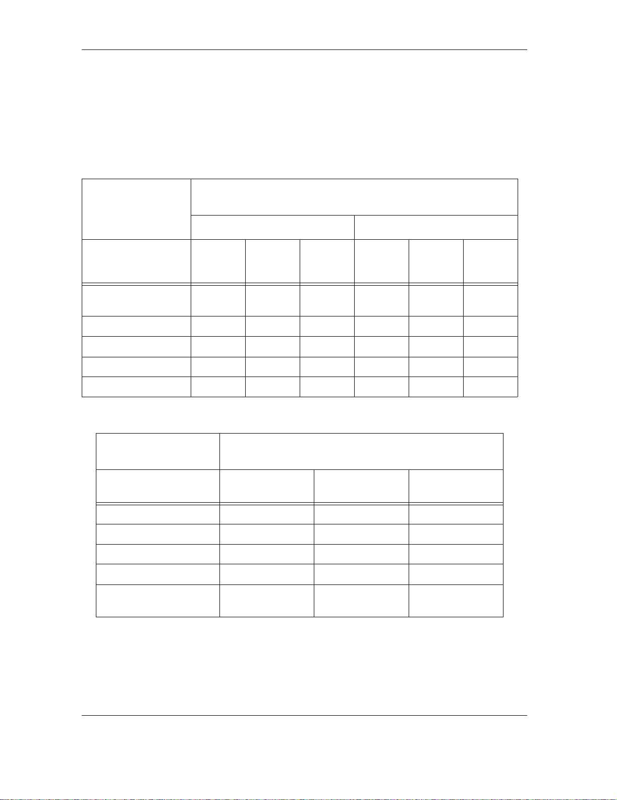
Specifications
4.5.3
4.5.3 Power Requirements
4.5.34.5.3
Power Require ments
Power Require mentsPower Require ments
Table 4-5 lists the voltages and typical average corresponding currents for the
various modes of operation of the Quantum Fireball Plus AS hard disk drives.
Table 4-5
Table 4-5 Typical Power and Current Consumption
Table 4-5 Table 4-5
MODE OF
MODE OF
MODE OF MODE OF
OPERATION
OPERATION
OPERATIONOPERATION
MODEL NUMB E R
MODEL NUMB E R
MODEL NUMB E RMODEL NUMB E R
Startup
1
(peak)
3
Idle
Maximum Seeking
Standby
5
4
Read/Write On T r ack
MODE OF OPERATION
MODE OF OPERATION
MODE OF OPERATIONMODE OF OPERATION
2
+5V
+5V+5V
30.0/
30.0/
30.0/30.0/
40.0GB
40.0GB
40.0GB40.0GB
(2-Disks)
(2-Disks)
(2-Disks)(2-Disks)
10.2/20.5
10.2/20.5
10.2/20.5 10.2/20.5
GB
GB
GBGB
(1-Disk)
(1-Disk)
(1-Disk)(1-Disk)
TYPICAL AVERAGE CURRENT
TYPICAL AVERAGE CURRENT
TYPICAL AVERAGE CURRENTTYPICAL AVERAGE CURRENT
(mAmps RMS unless otherwise noted)
(mAmps RMS unless otherwise noted)
(mAmps RMS unless otherwise noted)(mAmps RMS unless otherwise noted)
+12V
+12V +5V
+12V+12V
30.0/
30.0/
30.0/30.0/
40.0GB
40.0GB
40.0GB40.0GB
(2-Disks)
(2-Disks)
(2-Disks)(2-Disks)
60.0 GB
60.0 GB
60.0 GB60.0 GB
(3-Disks)
(3-Disks)
(3-Disks)(3-Disks)
10.2/20.5
10.2/20.5
10.2/20.5 10.2/20.5
GB
GB
GBGB
(1-Disk)
(1-Disk)
(1-Disk)(1-Disk)
1775 1800 1900 480 480 480
258 325 380 427 429 424
920 935 960 432 438 439
11 11 11 85 85 85
6
281 345 394 502 506 505
2
(WATTS)
TYPICAL AVERAGE POWER
TYPICAL AVERAGE POWER
TYPICAL AVERAGE POWERTYPICAL AVERAGE POWER
(WATTS)
(WATTS)(WATTS)
60.0 GB
60.0 GB
60.0 GB60.0 GB
(3-Disks)
(3-Disks)
(3-Disks)(3-Disks)
MODEL NUMB E R
MODEL NUMB E R
MODEL NUMB E RMODEL NUMB E R
10.2/20.5 GB
10.2/20.5 GB10.2/20.5 GB
(1-Disk)
(1-Disk)
(1-Disk)(1-Disk)
30.0/40.0GB
30.0/40.0GB
30.0/40.0GB30.0/40.0GB
(2-Disks)
(2-Disks)
(2-Disks)(2-Disks)
10.2/20.5 GB
Startup1 (peak) 23.7 24.0 25.2
3
Idle
Maximum Seeking
Standby
4
4
Read/Write On Track
(peak)
6
5.2 6.0 6.7
13.2 13.4 13.7
0.6 0.6 0.6
5.9 6.7 7.3
1. Current is rms except for startup. Startup current is the typical peak current of
the peaks greate r than 10 ms in dura tion. Thi s power is required fo r less th an 6
seconds.
2. Power requirements reflect nominal for +12V and +5V power.
4-6 Quantum Fireball Plus AS 10.2/20.5/30.0/40.0/60.0 GB AT
60.0 GB
60.0 GB
60.0 GB60.0 GB
(3-Disks)
(3-Disks)
(3-Disks)(3-Disks)
Page 41

3. Idle mode is in effect when the drive is not reading, writing, seeking, or
executing any commands. A portion of the R/W circuitry is powered down, the
motor is up to speed and the Drive Ready condition exists.
4. Maximum seeking is defined as continuous random seek operations with
minimum controller delay.
5. Standby mode is defined as when the motor is stopped, the actuator is parked,
and all electronics exc ept the interf ace control are in low power s tate. St andby
occurs after a programma ble time-out after th e last host access. Drive ready and
seek complete status exist. The drive lea ves standby upon receipt o f a command
that requires disk access or upon receiving a spinup command.
6. Read/Write On Track is defined as 50% read operations and 50% write
operations on a single physical track.
4.6
4.6 ACOUSTICS
4.64.6
ACOUSTICS
ACOUSTICSACOUSTICS
Table 4-6 specifies the acoustical characteristics of the Quantum Fireball Plus AS
10.2/20.5/30.0/40.0/60.0 GB AT hard disk drive. The acoustics are measured in an
anechoic chamber with background noise at least <10dBA less than th e expected
sound pressure Lp(A). To distinguish between sound power and sound pressure
standards, sound power Lw(A) is specified in Bels. The relationship between bels
and dBA for sound power is 1 bel = 10dBA.
Specifications
OPERATING MODE
OPERATING MODE
OPERATING MODEOPERATING MODE
Idle On Track
Seeking Random
Normal Mode
Quiet Mode
1
Note:
1. The statistical values (mean and mean +3 sigma) are determined separately for
Table 4-6
Table 4-6 Acoustical Characteristics—Sound Power
Table 4-6 Table 4-6
MEASURED SOUND
MEASURED SOUND
MEASURED SOUND MEASURED SOUND
POWER (MEAN)
POWER (MEAN)
POWER (MEAN)POWER (MEAN)
3.0 Bels (1-Disk)
3.2 Bels (2-Disk)
3.3 Bels (3-Disk)
1
3.6 Bels
3.4 Bels
each drive capacity. A sample lot of 30 drives is recommended for each capacity.
MEASURED SOUND
MEASURED SOUND
MEASURED SOUND MEASURED SOUND
POWER
POWER (Mean + 3 Sigma)
POWER POWER
(Mean + 3 Sigma)
(Mean + 3 Sigma)(Mean + 3 Sigma)
3.3 Bels (1-Disk)
3.5 Bels (2-Disk)
3.6 Bels (3-Disk)
3.9 Bels
3.7 Bels
Quantum Fireball Plus AS 10.2/20.5/30.0/40.0/60.0 GB AT 4-7
Page 42

Specifications
4.7
4.7 MECHANICAL
4.74.7
4.8
4.8 ENVIRONMENTAL CO NDITIONS
4.84.8
MECHANICAL
MECHANICALMECHANICAL
Quantum Fireball Plus AS hard disk drives are designed to meet the form factor
dimensions of the SFF committee specification SFF8300.
Height: 26.1 mm maximum
Width: 101.6 ± 0.25mm
Depth: 147 mm maximum
Weight: 1.35 lb
ENVIRONMENTAL CONDITIONS
ENVIRONMENTAL CONDITIONSENVIRONMENTAL CONDITIONS
Table 4-7 summarizes the environmental specifications of the Quantum Fireball
Plus AS hard disk drives.
Table 4-7
Table 4-7 Environmental Specifications
Table 4-7 Table 4-7
PARAMETER
PARAMETER OPERATING
PARAMETERPARAMETER
OPERATING NON-OPERATING
OPERATINGOPERATING
NON-OPERATING
NON-OPERATINGNON-OPERATING
Temperature
(Non-condensing)
Temperature Gradient
(Non-condensing)
Humidity
Maximum Wet Bulb
Temperature
Humidity Gradient 10% / hour 10% / hour
Altitude
Altitude Gradient 1.5 kPa/min 8 kPa/min
1
2
(Non-condensing)
3, 4
1. Maximum operating temperature must not exceed the driv e at any poi nt along
the drive form factor env elope. Airf low or other me ans must be used as needed
to meet this requirement.
2. The humidity range shown is applicable for temperatures whose combination
does not result in condensation in violation of the wet bulb specifications.
3. Altitude is relative to sea level.
5° to 55°C
(41° to 131°F)
20°C/hr maxi mum
(68°F/hr)
10% to 85% RH
30°C (86°F)
–200 m to 3,000 m
(–650 to 10,000 ft.)
-40° to 65°C
(-40° to 149°F)
30°C/hr maxi mum
(86°F/hr)
5% to 95% RH
40°C (104°F)
–200 m to 12,000 m
(–650 to 40,000 ft.)
4. The specified drive uncorrectable error rate will not be exceeded over these
conditions.
4-8 Quantum Fireball Plus AS 10.2/20.5/30.0/40.0/60.0 GB AT
Page 43

4.9
4.9 SHOCK AND VIBRATION
4.94.9
SHOCK AND VIBRATION
SHOCK AND VIBRATIONSHOCK AND VIBRATION
The Quantum Fireball Plus AS 10.2/20.5/30.0/40.0/60.0 GB AT hard disk drives
can withstand levels of shock and vibration applied to any of its three mutually
perpendicular axes, or principal base axis, as specified in Table 4-8. A functioning
drive can be subjected to specified operating levels of shock and vibration. When a
drive has been subjected to specified nonoperating levels of shock and vibration,
with power to the drive off, there will be no loss of user data at power on.
When packed in its 1-pack shipping container, the Quantum Fireball Plus AS drives
can withstand a drop from 30 inches onto a concrete surface on any of its surfaces,
six edges, or three corners. The 20-pack shipping container can withstand a drop
from 30 inches onto a concrete surface on any of its surfaces, six edges, or three
corners.
Table 4-8
Table 4-8 Shock and Vibration Specifications
Table 4-8 Table 4-8
Specifications
SHOCK
SHOCK
SHOCKSHOCK
1
OPERATING
OPERATING NONOPERATING
OPERATINGOPERATING
Translational
1/2 sine wave 30.0 Gs, 2 ms (write)
63.0 Gs, 2 ms (read)
Rotational 2 ms applied at
2,000 rad/sec
2
20,000 rad/sec2
geometry center of the drive
Vibration
1
Translational
Random Vibration (G
Sine wave (peak to peak)
2
/Hz)
0.004 (10 – 300Hz)
.5 G P-P 5-400 Hz
1/4 octave per minute sweep
Rotational
12.5 rad/sec
2
(10 – 300Hz)
1. The specified drive unrecovered error rate will not be exceeded over these
conditions.
NONOPERATING
NONOPERATINGNONOPERATING
300 Gs, 2 ms
110 Gs, 1ms
0.05 (10 – 300 Hz)
2G P-P 5–500 Hz
1 octave per minute sweep
Quantum Fireball Plus AS 10.2/20.5/30.0/40.0/60.0 GB AT 4-9
Page 44

Specifications
4.10
4.10 HANDLING THE DRIVE
4.104.10
HANDLING THE DRIVE
HANDLING THE DRIVEHANDLING THE DRIVE
Before handling the Quantum hard disk drive some precautions must to be taken
to ensure that the drive is not damaged. Use both hands while handling the drive
and hold the drive by its edges. Quantum drives are designed to withstand normal
handling, however, hard drives can be damaged by electrostatic discharge (ESD),
dropping the drive, rough handling, and mishandling. Use of a properly grounded
wrist strap to the earth is strongly recommended. Always keep the drive inside its
special antistatic bag until ready to install.
Note: To avoid causing any damage to the drive do not touch the
4.11
4.11 RELIABILITY
4.114.11
RELIABILITY
RELIABILITY RELIABILITY
Mean Time Between Failures (MTBF): The projected field MTBF is 625,000
Component Life: 3 years
Preventive Maintenance (PM): Not required
Start/Stop: 40,000 cycles at ambient temperature
Note: CSS specification assumes a duty cycle of one power off oper-
Printed Circuit Board (PCB) or any of its components when
handling the drive.
ation for every one idle mode spin downs.
hours. The Quantum MTBF numbers
represent Bell-Core TR-332 Issue #6,
December 1997 MTBF predictions and
represent the minimum MTBF that
Quantum or a customer would expect
from the drive.
(minimum)
4-10 Quantum Fireball Plus AS 10.2/20.5/30.0/40.0/60.0 GB AT
Page 45
4.12
4.12 ELECTROMAGNETIC SUSCEPTIBILITY
4.124.12
4.13
4.13 SPINDLE IMBALANCE
4.134.13
4.14
4.14 DISK ERRORS
4.144.14
ELECTROMAGNETIC SUSCEPTIBILITY
ELECTROMAGNETIC SUSCEPTIBILITYELECTROMAGNETIC SUSCEPTIBILITY
E Field: 3Volts/meter at <100 MHz.
B Field: As per standard EN61004-8
SPINDLE IMBALANCE
SPINDLE IMBALANCESPINDLE IMBALANCE
0.5 g-mm maximum
(This is approxim ately equivalent to 0.04 G emitted vibrations)
DISK ERRORS
DISK ERRORSDISK ERRORS
Table 4-9 provides the error rates for the Quantum Fireball Plus AS hard disk
drives.
Table 4-9
Table 4-9 Error Rates
Table 4-9 Table 4-9
ERROR TYPE
ERROR TYPE MAXIMUM NUMBER OF ERRORS
ERROR TYPEERROR TYPE
MAXIMUM NUMBER OF ERRORS
MAXIMUM NUMBER OF ERRORSMAXIMUM NUMBER OF ERRORS
Specifications
Retry recovered read errors
Unrecovered read errors
Seek errors
3
1. Retry recovered read errors are errors whic h require retries for dat a correction.
Errors corrected by ECC on-the-fly are not considered recovered read errors.
Read on arrival is disabled to meet this specification. Errors corrected by the
thermal asperity correctio n are not considered recovered read errors.
2. Unrecovered read errors are errors that are not correctable using ECC or
retries. The drive terminates retry reads either when a repeating error pattern
occurs, or after the programmed limit for unsuccessful retries and the
application of quadruple-burst error correction.
3. Seek errors occur when the actuator fails to reach (or remain) over the
requested cylinder and the drive requires the execution of a full recalibration
routine to locate the requested cylinder.
Note: Error rates are for worst case temperature and voltage.
2
1
1 event per 109 bits read
1 event per 1014 bits read
1 error per 106 seeks
Quantum Fireball Plus AS 10.2/20.5/30.0/40.0/60.0 GB AT 4-11
Page 46

Chapter 5
Chapter 5
Chapter 5Chapter 5
BASIC PRINCIPLES OF OPERATION
BASIC PRINCIPLES OF OPERATION
BASIC PRINCIPLES OF OPERATIONBASIC PRINCIPLES OF OPERATION
This chapter describes the operation of Quantum Fireball Plus AS AT hard disk
drives’ functional subsys tems. It is intended a s a guide to the operati on of the drive,
rather than a detailed theory of operation.
5.1
5.1 QUA NTUM FIREBALL PLUS AS DRIVE MECHANISM
5.15.1
QUANTUM FIREBALL PLUS AS DRIVE MECHANISM
QUANTUM FIREBALL PLUS AS DRIVE MECHANISMQUANTUM FIREBALL PLUS AS DRIVE MECHANISM
This section des cribes the drive mecha nism. Section 5.2 describes the drive
electronics. The Quantum F ireball Plus AS hard dis k drives consist of a mech anical
assembly and a PCB as shown in Figure 5-1.
The head/disk assembly (HDA) contains the mechanical subassemblies of the
drive, which are sealed under a metal cover. The HDA consists of the following
components:
•Base casting
• DC motor assembly
• Disk stack assembly
•Headstack assembly
• Rotary positioner assembly
• Automatic actuator lock
•Air filter
The drive is assembled in a Class-100 clean room.
CAUTION:
CAUTION: To ensure that the air in the HDA remains free of
CAUTION:CAUTION:
contamination, never remove or adjust its cover
and seals. Tamp ering with the HDA wil l void you r
warranty.
Quantum Fireball Plus AS 10.2/20.5/30.0/40.0/60.0 GB AT 5-1
Page 47
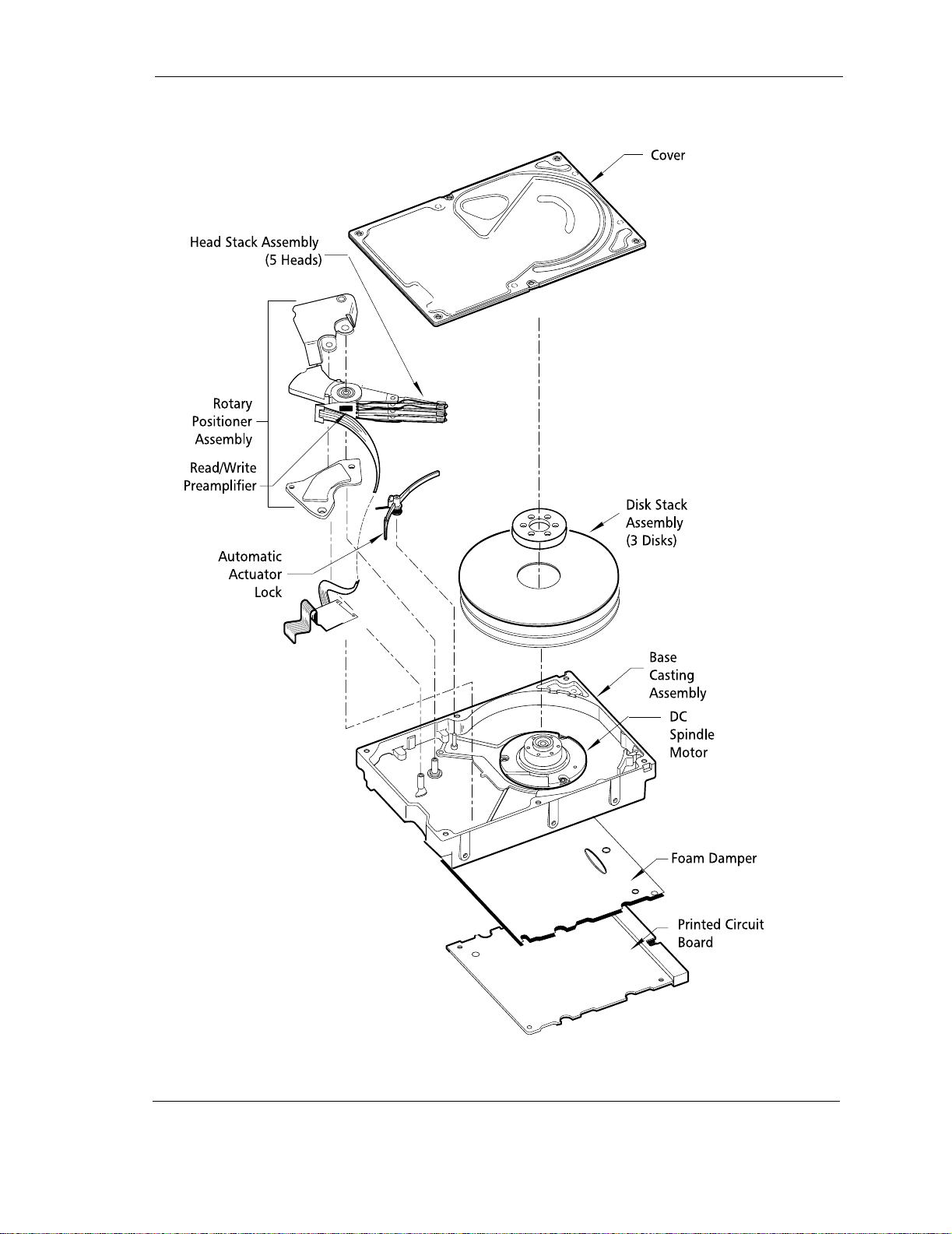
Basic Principles of Operation
Figure 5-1
Figure 5-1 Quantum Fireball Plus AS AT Hard Disk Drive Exploded View
Figure 5-1 Fi gure 5-1
Quantum Fireball Plus AS 10.2/20.5/30.0/40.0/60.0 GB AT 5-2
Page 48

Basic Principles of O per ation
5.1.1
5.1.1 Base Casting Assembly
5.1.15.1.1
5.1.2
5.1.2 DC Motor Assembly
5.1.25.1.2
5.1.3
5.1.3 Disk Stack Assemblies
5.1.35.1.3
Base Casting Assembly
Base Casting AssemblyBase Casting Assembly
A single-piece, e-coated, aluminum-alloy base casting provides a mounting surface
for the drive mechanism and PCB. The base casting also acts as the flange for the
DC motor assembly. To provide a contamination-free environment for the HDA, a
gasket provides a seal between the base casting, and the metal cover that encloses
the drive mechanism.
DC Motor Assembly
DC Motor AssemblyDC Motor Assembly
Integral with the base casting, the DC motor assembly is a fixed-shaft, brushless DC
spindle motor that drives the counter-clockwise rotation of the disks.
Disk Stack Assemblies
Disk Stack AssembliesDisk Stack Assemblies
The disk stack assembly in the Quantum Fireball Plus AS hard disk drives consist
of disks secured by a disk clamp. The aluminum-alloy disks have a sputtered thinfilm magnetic coating.
A carbon overcoat lubricates the disk surface. This prevents head and media wear
due to head contact with the disk surface during head takeoff and landing. Head
contact with the disk surface occurs only in the landing zone outside of the data
area, when the disk is not rotating at full speed. The landing zone is located at the
inner diameter of the disk, beyond the last cylinder of the data area.
Table 5-1
Table 5-1 Cylinder Contents
Table 5-1 Table 5-1
NUMBER
CYLINDER
CYLINDER
CYLINDERCYLINDER
CONTENTS
CONTENTS
CONTENTSCONTENTS
System Data 0 65 345 302.0
1
ZONE
ZONE
ZONEZONE
1 2348 694 490.0
2 2342 690 486.7
3 2342 676 476.9
4 2342 666 466.7
5 2342 651 456.7
6 2342 636 446.7
7 2342 616 433.3
8 2342 598 420
9 2342 592 406.2
10 2342 551 387.7
11 2342 522 365.7
12 2342 493 344.0
13 2342 453 317.7
14 2342 419 292.5
15 2342 375 262.5
NUMBER
NUMBER NUMBER
OF TRACKS
OF TRACKS
OF TRACKSOF TRACKS
SECTORS
SECTORS
SECTORS SECTORS
PER TRACK
PER TRACK
PER TRACKPER TRACK
DATA RATE
DATA RATE
DATA RATEDATA RATE
1. For user data, zone 15 is the innermost zone and zone 1 is the outermost zone.
5-3 Quantum Fireball Plus AS 10.2/20.5/30.0/40.0/60.0 GB AT
Page 49

5.1.4
5.1.4 Headstack Assembly
5.1.45.1.4
5.1.5
5.1.5 Rotary Positioner Assembly
5.1.55.1.5
Headstack Assembly
Headstack AssemblyHeadstack Assembly
The headstack assembly consists of read/write heads, head arms, and a coil joined
together by insertion molding to form a rotor subassembly, bearings, and a flex
circuit. Read/write heads mounted to spring-steel flexures are swage mounted onto
the rotary positioner assembly arms.
The flex circuit exits the HDA through the base casting. A cover gasket seals the
gap. The flex circuit connects the headstack assembly to the PCB. The flex circuit
contains a read preamplifier/write driver IC.
Rotary Positioner Assembly
Rotary Positioner AssemblyRotary Positioner Assembly
The rotary positioner, or rotary voice-coil actuator, is a Quantum-proprietary
design that consists of upper and lower permanent magnet plates, a rotary singlephase coil molded around the headstack mounting hub, and a bearing shaft. The
single bi-polar magnet consists of two alternating poles and is bonded to the magnet
plate. A resilient crash stop prevents the heads from being driven into the spindle
or off the disk surface.
Current from the power amplifier induces a magnetic field in the voice coil.
Fluctuations in the field around the permanent magnet cause the voice coi l to move.
The movement of the voice coil positions the heads over the requested cylinder.
Basic Principles of Operation
5.1.6
5.1.6 Automatic Actuator Lock
5.1.65.1.6
Automatic Actuator Lock
Automatic Actuator LockAutomatic Actuator Lock
To ensure data integrity and prevent damage during shipment, the drive uses a
dedicated landing zone, an actuator magnetic retract, and Quantum’s patented
Airlock
are not rotatin g. It consists of an air vane mounted ne ar the perimeter of the disk
stack, and a locking arm that restrains the actuator arm assembly.
When DC power is applied to the motor and the disk stack rotates, the rotation
generates an airflow on the surface of the disk. As the flow of air across the air vane
increases with disk rotation, the locking arm pivots away from the actuator arm,
enabling the headstack to move out of the landing zone. When DC power is
removed from the motor, an electronic return mechanism automatically pulls the
actuator into the landing zone, where the magnetic actuator retract force holds it
until the Airlock closes and latches it in place.
®
. The Airlock holds the headstack in the la nding zo ne whenev er the d isks
Quantum Fireball Plus AS 10.2/20.5/30.0/40.0/60.0 GB AT 5-4
Page 50

Basic Principles of O per ation
5.1.7
5.1.7 Air Filtration
5.1.75.1.7
5.2
5.2 DRIVE ELECTRONICS
5.25.2
Air Filtration
Air FiltrationAir Fil tration
The Quantum Fireball Plus AS AT hard disk drives are Wi nchester-type drives. The
heads fly very clos e to the media surface. Therefore, it is essential that the air
circulating within the drive be kept free of particles. Quantum assembles the drive
in a Class-100 purified air environment, then seals the drive with a metal cover.
When the drive is in use, the rotation of the disks forces the air inside of the drive
through an internal 0.3 micron filter. The internal HDA cavity pressure equalizes
to the external pressure change by passing air through a 0.3 micron, carbon
impregnated breather filter.
DRIVE ELECTRONICS
DRIVE ELECTRONICSDRIVE ELECTRONICS
Advanced circuit (Very Large Scale Integration) design and the use of miniature
surface-mounted devices and proprietary VLSI components enable the drive
electronics, including the ATA bus interface, to reside on a single printed circuit
board assembly (PCBA).
Figure 5-2 contains a simplified block diagram of the Quantum Fireball Plus AS
hard disk drive electronics.
The only electrical component not on the PCBA is the PreAmplifier and Write
Driver IC. It is on the flex circuit (inside of the sealed HDA). Mounting the
preamplifier as close as possible to the read/write heads improves the signal-tonoise ratio. The flex circuit (including the PreAmplifier and Write Driver IC)
provides the electr ical connection between the PCB, the rota ry positioner assembly,
and read/write heads.
Figure 5-2
Figure 5-2 Quantum Fireball Plus AS AT Hard Disk Drive Block Diagram
Figure 5-2 Fig ure 5-2
5-5 Quantum Fireball Plus AS 10.2/20.5/30.0/40.0/60.0 GB AT
Page 51

Basic Principles of Operation
5.2.1
5.2.1 Integrated µProcessor, Disk Controller and ATA Interface
5.2.15.2.1
Integrated µProcessor, Disk Controller and ATA Interface
Integrated µProcessor, Disk Controller and ATA Interface Integrated µProcessor, Disk Controller and ATA Interface Electronics
Electronics
ElectronicsElectronics
The µProce ssor , Dis k C ont rol ler , and ATA Inte rfac e e lect ro nics are cont ain ed i n a
proprietary ASIC developed by Quantum, as shown below in Figure 5-3.
Figure 5-3
Figure 5-3 Block Diagram
Figure 5-3 Figure 5-3
Quantum Fireball Plus AS 10.2/20.5/30.0/40.0/60.0 GB AT 5-6
Page 52

Basic Principles of O per ation
The integrated µProcessor, Disk Controller, and ATA Interface Electronics have
nine functional modules (described below):
•µProcessor
• Digital Synchronous Spoke (DSS)
• Error Correction Code (ECC) Control
• Formatter
• Buffer Controller
• Servo Controller, including PWM
•Serial Interface
• ATA Interface Controller
• Motor Controller
5.2.1.1
5.2.1.1 µProcessor
5.2.1.15.2.1.1
µProcessor
µProcessor µProcessor
The µProcessor core provi des local processor services t o the drive electronics under
program control. The µPro cessor manages the resources of the Disk Controller, and
ATA Interface internally. It also manages the Read/Write ASIC (Application
Specific Integrated Circuit), and the Spindle/VCM driver externally.
5.2.1.2
5.2.1.2 Digital Synchronous Spoke
5.2.1.25.2.1.2
Digital Synchronou s Spoke
Digital Synchronou s SpokeDigital Synchronous Spoke
The DSS decodes servo information written on the drive at the factory to determine
the position of the read/write head. It interfaces with the read/write channel,
process timing and position information, and stores it in registers that are read by
the servo firmware.
5.2.1.3
5.2.1.3 Error Correction Code (ECC) Control
5.2.1.35.2.1.3
Error Correction Code (ECC) Control
Error Correction Code (ECC) ControlError Correction Code (ECC) Control
The Error Correction Code (ECC) Contr ol block uti lizes a Reed-So lomon encode r/
decoder circuit that is used for disk read/write operations. It uses a total of 44
redundancy bytes organized as 40 ECC (Error Correction Code) bytes with one
interleave, and four cross-check bytes. The ECC uses ten bits per symbol and one
interleave. This is guaranteed to correct 150 bits and as many as 160 bits in error.
5.2.1.4
5.2.1.4 Formatter
5.2.1.45.2.1.4
Formatter
FormatterFormatter
The Formatter contro ls the operatio n of t he read and wri te channel portio ns of th e
ASIC. To initiate a disk operation, the µProcessor loads a set of commands into the
WCS (writable control s tore) r egist er. L oading a nd manipu lat ing the WCS is do ne
through the µProcessor Interface registers.
The Formatter also directly drives the read and write gates (
Mode Interface of the Read/Write ASIC and the R/W Preamplifier, as well as
passing write data to the Precompensator circuit i n the Read/Write ASIC.
RG, WG) and Command
5-7 Quantum Fireball Plus AS 10.2/20.5/30.0/40.0/60.0 GB AT
Page 53

5.2.1.5
5.2.1.5 Buffer Controller
5.2.1.55.2.1.5
5.2.1.6
5.2.1.6 Servo Processor
5.2.1.65.2.1.6
5.2.1.7
5.2.1.7 Read/Write Interface
5.2.1.75.2.1.7
Buffer Controller
Buffer ControllerBuffer Controller
The Buffer Controller supports a 2 MB buffer, which is organized as 1M x 16 bits.
The 16-bit width i mplementa tion provides a 60 MB /s maxim um buffe r bandwidt h.
This increased bandwidth allows the µProcessor to have direct access to the buffer,
eliminating the need for a separate µProcessor RAM IC.
The Buffer Controlle r support s both drive a nd host address rollo ver and reload ing,
to allow for buffer segmentation. Drive and host addresses may be separately loaded
for automated read/write functions.
The Buffer Controller operates under the direction of the µProcessor.
Servo Processor
Servo ProcessorServo Proces sor
The Servo Processor in t he Read Write C hannel ASIC provid es servo data recovery
and burst demodulation to extract the actuator position information. This
information is processed in the controller ASIC/microprocessor, and a control
signal is output to the VCM in the Power ASIC. This controls the current in the
actuator coil which controls the position of the actuator.
Read/Write Interface
Read/Write InterfaceRead/Write Interface
The Read/Write interface allows the integrated µprocessor, disk controller to
communicate with the Read/Write chip.
Basic Principles of Operation
5.2.1.8
5.2.1.8 ATA Interface Controller
5.2.1.85.2.1.8
5.2.1.9
5.2.1.9 Motor Controller
5.2.1.95.2.1.9
5.2.2
5.2.2 Read/Write ASIC
5.2.25.2.2
ATA Interface Controller
ATA Interface ControllerATA Interface Controller
The ATA Interface Controller portion of the ASIC provides dat a handling, bus
control, and transfer management services for the ATA interface. Configuration
and control of the interface is accomplished by the µController across the MAD
bus. Data transfer operations are controlled by the Buffer Controller module.
Motor Controller
Motor ControllerMotor Controller
The Motor Controller controls the spi ndle and voice coil motor (VCM) mechanism
on the drive.
Read/Write ASIC
Read/Write ASICRead/Write ASIC
The Read/Write ASIC integrates an Advanced Partial Response Maximum
Likelihood (PRML) processor, a selectable code rate Encoder-Decoder (ENDEC),
and a Servo Processor with data rates up to 340 MHz. Programming is done
through a fast 40 MHz serial interface. The controller and data interface through an
8-bit wide data interface. The Read/Write ASIC is a low power 3.3 Volts, single
supply, with selective power down capabilities.
The Read/Write ASIC comprises 12 main functional modules (described below):
•Pre-Compensator
• Variable Gain Amplifier (VGA)
•Butterworth Filter
•FIR Filter
• Flash A/D Converter
•Viterbi Detector
•ENDEC
• Servo Processor
Quantum Fireball Plus AS 10.2/20.5/30.0/40.0/60.0 GB AT 5-8
Page 54

Basic Principles of O per ation
•Clock Synthesizer
•PLL
•Serial Interface
• TA Detection and Correction
5.2.2.1
5.2.2.1 Pre-Compensator
5.2.2.15.2.2.1
Pre-Compensator
Pre-CompensatorPre-Compensator
The pre-compensator intro duces pre-compensati on to the write d ata received fr om
the sequencer module in the DCIIA. The pre-compensated dat a is then passed to
the R/W Pre-Amplifier and written to the disk. Pre-compensation reduces the write
interference from adjacent write bit.
5.2.2.2
5.2.2.2 Variable Gain Amplifier (VGA)
5.2.2.25.2.2.2
Variable Gain Amplifier (VGA)
Variable Gain Amplifier (VGA)Variable Gain Amplif ier (VGA)
Digital and analog controlled AGC function with input attenuator for extended
range.
5.2.2.3
5.2.2.3 Butterworth Filter
5.2.2.35.2.2.3
Butterworth Filter
Butterworth FilterButterworth Filter
Continuous time data filter which can be programmed for each zone rate.
5.2.2.4
5.2.2.4 FIR (Finite I mpulse Response) Filter
5.2.2.45.2.2.4
FIR (Finite Impulse Response) Filter
FIR (Finite Impulse Response) FilterFIR (Finite Impulse Response) Filter
Digitally controlled and programmable filter for partial response signal
conditioning.
5.2.2.5
5.2.2.5 Flash A/D Converter
5.2.2.55.2.2.5
Flash A/D Converter
Flash A/D ConverterFlash A/D Converter
Provides very high speed digitization of the processed read signal.
5.2.2.6
5.2.2.6 Viterbi Detector
5.2.2.65.2.2.6
Viterbi Detector
Viterbi DetectorViterbi Detector
Decodes ADC result into binary bit stream.
5.2.2.7
5.2.2.7 ENDEC
5.2.2.75.2.2.7
ENDEC
ENDECENDEC
Provides 16/17 or 24/25 code conversion to NRZ. Includes preamble and sync
mark generation and detection.
5.2.2.8
5.2.2.8 Servo Processor
5.2.2.85.2.2.8
Servo Processor
Servo ProcessorServo Processor
Servo processor with servo data recovery and burst demodulation.
5.2.2.9
5.2.2.9 Clock Synthesizer
5.2.2.95.2.2.9
Clock Synthesizer
Clock SynthesizerClock Synthesizer
Provides programmable frequencies for each zone data rate.
5.2.2.10
5.2.2.10 PLL
5.2.2.105.2.2.10
PLL
PLLPLL
Provides digital read clock recovery.
5.2.2.11
5.2.2.11 Serial Interface
5.2.2.115.2.2.11
Serial Interface
Serial InterfaceSerial Interfac e
High speed interface for digital control of all internal blocks.
5.2.2.12
5.2.2.12 TA Detection and Correction
5.2.2.125.2.2.12
TA Detection and Correction
TA Detection and CorrectionTA Detection and Correction
Detects thermal asperities’ defective sectors and enables thermal asperity
recoveries.
5-9 Quantum Fireball Plus AS 10.2/20.5/30.0/40.0/60.0 GB AT
Page 55

5.2.3
5.2.3 PreAmplifier and Write Driver
5.2.35.2.3
5.3
5.3 FIRMWARE F EATURES
5.35.3
5.3.1
5.3.1 Disk Caching
5.3.15.3.1
PreAmplifier and Write Driver
PreAmplifier and Write DriverPreAmplifier and Write Driver
The PreAmplifier and Write Driver provides write driver and read pre-amplifier
functions, and R/W head selectio n. The write driver recei ves precompensated write
data from the PreCompensator module in the Read/Write ASIC. The write driver
then sends this data to the heads in the form of a corresponding alternating current.
The read pre-amplifier amplifies the low-amplitude voltages generated by the R/W
heads, and transmits them to the VGA module in the Read/Write ASIC. Head select
is determined by the controller. The preamp also contains internal compensation
for thermal asperity induced amplitude variation.
FIRMWARE FEATURES
FIRMWARE FEATURESFIRMWARE FEATURES
This section describes the following firmware features:
• Disk caching
• Head and cylinder skewing
• Error detection and correction
• Defect management
Disk Caching
Disk CachingDisk Caching
Basic Principles of Operation
The Quantum Fireball Plus AS AT hard disk drives incorporate DisCache, a
1.9 MB disk cache, to enhance drive performance. This integrated feature is
user-programmable and can significantly improve system throughput. Read
and write caching can be enabled or disabled by using the Set Configuration
command.
5.3.1.1
5.3.1.1 Adaptive Caching
5.3.1.15.3.1.1
5.3.1.2
5.3.1.2 Read Cache
5.3.1.25.3.1.2
Adaptive Caching
Adaptive CachingAdaptive Caching
The cache buffer for the Quantum Fireball Plus AS drives features adaptive
segmentation for more efficient use of the buffer’s RAM. With this feature, the
buffer space used for r ead and write operatio ns is dynamicall y allocat ed. The cache
can be flexibly divided into several segments under program control. Each segment
contains one cache entry.
A cache entry consists of the requested read data plus its corresponding prefetch
data. Adaptive segmentation allows the drive to make optimum use of the buffer.
The amount of stored data can be increased.
Read Cache
Read CacheRead Cache
DisCache anticipates host-system requests for data and stores that data for faster
access. When the host requests a particular segment of data, the caching feature
uses a prefetch strategy to “look ahead”, and automatically store the subsequent
data from the di sk int o high-sp eed RAM. I f the h ost req uests this subs equent d ata,
the RAM is accessed rather than the disk.
Since typically 50 percent or mo re of all di sk requests are s equential, ther e is a high
probability that subsequent data requested will be in the cache. This cached data
can be retrieved in microseconds rather than milliseconds. As a result, DisCache
can provide substantial time savings during at least half of all disk requests. In these
instances, D isCache co uld save mo st of the d isk transac tion time b y eliminat ing the
seek and rotational latency delays that dominate the typical disk transaction. For
example, in a 1K data transfer, these delays make up to 90 percent of the elapsed
time.
Quantum Fireball Plus AS 10.2/20.5/30.0/40.0/60.0 GB AT 5-10
Page 56

Basic Principles of O per ation
DisCache works by continuing to fill its cache memory with adjacent data after
transferring data requested by the host. Unlike a noncaching controller, Quantum’s
disk controller continues a read operation after the requested data has been
transferred to t he host s yste m. Th is re ad o pera t ion te rminat es aft er a pro gra mmed
amount of subsequent data has been read into the cache segment.
The cache memory consists of a 1.9 MB DRAM buffer allocated to hold the data,
which can be directly accessed by the host by means of the READ and WRITE
commands. The memory functions as a group of segments with rollover points at
the end of cache memory. The unit of data stored is the logical block (that is, a
multiple of the 512 byte sector). Therefore, all accesses to the cache memory must
be in multiples of the sector size. Almost all non-read/write commands force
emptying of the cache:
5.3.1.3
5.3.1.3 Write Cache
5.3.1.35.3.1.3
Write Cache
Write CacheWrite Cache
When a write command is executed wit h write caching enabled, the dr ive stores the
data to be written in a DRAM cache buffer, and immediately sends a GOOD
STATUS message to the host before the data is actually written to the disk. The
host is then free to move on to other tasks, such as preparing data for the next data
transfer, without having to wait for the drive to seek to the appropriate track, or
rotate to the specified sector.
While the host i s prep ar ing da ta f or th e nex t tr ans fe r, t he d ri ve imme dia tely wr it es
the cached data to the disk.
WriteCache allows data to be transferred in a continuous flow to the drive, rather
than as individual blocks of data separated by disk access delays. This is achieved
by taking advantage of the ability to write blocks of data sequentially on a disk that
is formatted with a 1:1 interleave. This means that as the last byte of data is
transferred out of the write cache and the head passes over the next s e ctor of the
disk, the first byte of the of the next block of data is ready to be transferred, thus
there is no interruption or delay in the data transfer process.
The WriteCache algor ithm f il ls t he cach e buffer wi th new dat a fro m t he host wh il e
simultaneously transferring data to the disk that the host previously stored in the
cache.
5.3.1.4
5.3.1.4 Performance Benefits
5.3.1.45.3.1.4
Performance Benefits
Performance BenefitsPerformance Benefits
In a drive without DisCache, there is a delay during sequential reads because of the
rotational latency, even if the disk actuator already is positioned at the desired
cylinder. DisCache eliminates this rotational latency time (4.17 ms on average)
when requested data resides in the cache.
Moreover, the disk must often service requests from multiple processes in a
multitasking or multiuser environment. In these instances, while each process
might request data sequen tially, the disk drive must share time among all these
processes. In mo st d i sk driv es, th e he ads mus t move f rom one l oca tio n t o an ot he r.
With DisCache, even if another process interrupt s, the drive continues to a ccess the
data sequentially from its high-speed memory. In handling multiple processes,
DisCache achieves its most impressive performance gains, saving both seek and
latency time when desired data resides in the cache.
The cache can be flexibly divided into several segments under program contro l.
Each segment contains one cache entry. A cache entry consists of the requested
read data plus its corresponding prefetch data.
5-11 Quantum Fireball Plus AS 10.2/20.5/30.0/40.0/60.0 GB AT
Page 57

The requested read data takes up a certain amount of space in the cache segment.
Hence, the corresponding pre fetch data can essenti ally occupy the rest of the space
within the segment. The other factors determining prefetch size are the maximum
and minimum prefetch. The driv e’s prefetch algorithm dynamically controls the
actual prefetch value based on the current demand, with the consideration of
overhead to subsequent commands.
5.3.2
5.3.2 Head and Cylinder Skew ing
5.3.25.3.2
5.3.2.1
5.3.2.1 Head Skewing
5.3.2.15.3.2.1
5.3.2.2
5.3.2.2 Cylinder Skewing
5.3.2.25.3.2.2
Head and Cylinder Skewing
Head and Cylinder SkewingHead and Cylinder Skewing
Head and cylinder skewing in the Quantum Fireball Plus AS AT hard disk drives
minimize latency time and thus increases data throughput.
Head Skewing
Head SkewingHead Skewing
Head skewing reduces th e latency time that results when the drive must switch
read/write heads to access sequential data. A head skew is employed such that the
next logical sector of data to be accessed will be under the read/write head once the
head switch is made, and the data is ready to be accessed. Thus, when sequential
data is on the same cylinder but on a differ ent disk surface, a head sw itch is needed
but not a seek. Since the sequential head-switch time is well defined on the
Quantum Fireball Plus AS drives, the sector addresses can be optimally positioned
across track boundaries to minimize the latency time during a head switch. See
Table 5-2.
Cylinder Skewing
Cylinder SkewingCylinder Skewing
Cylinder skewing is also used to minimize the latency time associated with a singlecylinder seek. The next logical sector of data that crosses a cylinder boundary is
positioned on the drive such that after a single-cylinder seek is performed, and
when the drive is ready to continue accessing data, the sector to be accessed is
positioned directly under the read/write head. Therefore, the cylinder skew takes
place between the last sector of data on the last head of a cylinder, and the first
sector of data on th e f irst head of t he next cy li nder. Si nce s ingle-cy li nder s eek s are
well defined on the Quantum Fireball Plus AS drives, the sector addresses can be
optimally positioned across cylinder boundaries to minimize the latency time
associated with a single-cylinder seek. See Table 5-2.
Basic Principles of Operation
5.3.2.3
5.3.2.3 Skewing with ID-less
5.3.2.35.3.2.3
Skewing with ID-less
Skewing with ID-lessSkewing with ID-less
In the ID-less enviro nment, th e dri ve’s tra ck a nd cy li nder s kew ing will be based in
unit of wedges instead of the traditional sectors. The integrated µprocessor, disk
controller and ATA int erface contains a “Wedge S kew Register” to assist in the task
of skewing, where the skew offset must now be calculated with every read/write
operation. The firmware will program the skew offset into this register every time
the drive goes to a new track. The integrated µprocessor, disk controller and ATA
interface will then add this value to the wedge number in the ID calculator,
effectively relocating the “first” sector of the track away from the index. For
example, if without s kew, sector 0 is to be found following we dge 0, then if the skew
register is set to 10, sector 0 will be found following wedge 10.
Since the wedge-to-wed ge time is consta nt over the entire disk, a single se t of head
and cylinder skew off-sets will fulfill the requirement for all recording zones.
Quantum Fireball Plus AS 10.2/20.5/30.0/40.0/60.0 GB AT 5-12
Page 58

Basic Principles of O per ation
5.3.2.4
5.3.2.4 Skew Offsets
5.3.2.45.3.2.4
5.3.2.5
5.3.2.5 Runtime Calculation
5.3.2.55.3.2.5
Skew Offsets
Skew OffsetsSkew Offsets
Head Skew 1.75 ms 31
Cylinder Skew 1.20 ms 21
Note:
Note: Nominal wedge-to-wedge time of 56.25 ms is used. Worst case
Note:Note:
Runtime Calculation
Runtime CalculationRuntime Calculation
Since the wedge-to-wed ge time is consta nt over the entire disk, a single se t of head
and cylinder skew offsets will fulfill the requirement for all recording zones. The
formula used to compute the wedge skew for a given cylinder and head is:
instantaneous spindle variation (±0.12%) is used while calculating to provide a safety margin.
Wedge offsets are rounded to the closest whole number.
Table 5-2
Table 5-2 Skew Offsets
Table 5-2 Table 5-2
SWITCH TIME
SWITCH TIME WEDGE OFFSET
SWITCH TIMESWITCH TIME
WEDGE OFFSET
WEDGE OFFSETWEDGE OFFSET
Wedge skew = [C* ((# of heads – 1) * TS + CS) + H * TS] MOD 148
Where:C = Cylinder number
H = Head number
TS = Head Skew Offset
CS Cylinder Skew Offset
(wedges/track = 148)
5.3.3
5.3.3 Error Detection and Correction
5.3.35.3.3
5.3.3.1
5.3.3.1 Background Information on Error Correction Code and ECC On-the-Fly
5.3.3.15.3.3.1
Error Detection and Correction
Error Detection and CorrectionError Detection and Correction
As disk drive areal densities increase, obtaining extremely low error rates requires
a new generation of sophisti cated error correction codes. Quantum Fi reball Plus AS
hard disk drive series implement 320-bit Reed-Solomon error correction techni ques
to reduce the uncorrectable read block error rate to less than one bit in 1 x 10
read.
When errors occur, an automatic retry of 15 10-bit symbols and a more rigorous 16
10-bit symbols correction algorithm enable the correction of any sector with single
bursts, or up to sixteen multiple random one 10-bit symbol burst. In addition to
these advanced error correction capabilities, the drive uses an additional crosschecking code and algorithm to double check the main ECC co rrection. This greatly
reduces the probability of a miscorrection.
Background Information on Error Correction Code and ECC On-the-Fly
Background Information on Error Correction Code and ECC On-the-FlyBackground Information on Error Correction Code and ECC On-the-Fly
A sector on the Quantum Fireball Plus AS AT drive is comprised of 512 bytes of
user data, followed by four cross-checking (XC) bytes (32 bits), followed by 40 ECC
check bytes (320 bits) or 32 10-bit symbols. The four cross-checking bytes are used
to double check the main ECC correction and reduce the probability of
miscorrection. Errors of up to 150 bits within one sector can be corrected “on-thefly,” in real time as they occur, allowing a high degree of data integrity with no
impact on the drive’s performance.
14
bits
5-13 Quantum Fireball Plus AS 10.2/20.5/30.0/40.0/60.0 GB AT
Page 59

Basic Principles of Operation
The drive does not need to re-read a sector on the nex t disk revolution or apply ECC
for those errors that are corrected on-the-fly. Errors corrected in this manner are
invisible to the host system.
When errors cannot be corrected on-t he-fly, an automatic retry, and a more rigorous
16 10-bit symbols error correction algorithm enables the correction of any sector
with single bursts (up to 16 contiguous 10-bit symbols), or up to 16 multiple
random one 10-bit symbol burst errors. In addition to this error correction
capability, the drive’s implementation of an additional cross-checking code and
algorithm double checks the main ECC correction, and greatly decreases the
likelihood of misc or r ect io n.
The 32 ECC check symbols shown in Figure 5-4 are used to detect and correct
errors. The cross-checking and ECC data is computed and appended to the user
data when the sector is first written.
Figure 5-4
Figure 5-4 Sector Data Field with ECC Check Bytes
Figure 5-4 Figure 5-4
Because the ECC check symbols follow the cross checking bytes, errors found
within the cross-check ing byte s can be corre cte d. Due to th e pow e r and
sophistication of the code, errors found within the ECC check bytes can also be
corrected.
Each time a sector of data is read, the Quantum Fireball Plus AS drives will
generate a new set of ECC check symbols and cross-checking bytes from the user
data. These new check symbols are compared to the ones originally written to the
disk. The difference between the newly computed and original check symbols is
reflected in a set of 32 syndromes and three cross checking syndromes, which
correspond to the number of check symbols. If all the ECC syndrome values equal
zero, and cx syndrome value equals zero or 0FF, th e data was rea d with no erro rs ,
and the sector is transferred to the host system. If any of the syndromes do not equal
zero or OFF, an error has occurred. The type of correction the drive applies depends
on the nature and the extent of the error.
High speed on-the-fly error correction saves several milliseconds because there is
no need to wait for a disk revolution to bring the sector under the head for rereading.
5.3.3.2
5.3.3.2 ECC Error Handling
5.3.3.25.3.3.2
ECC Error Handling
ECC Error HandlingECC Error Handling
When a data error occurs, the Quantum Fir eball Plus AS hard disk driv es check to
see if the error is correctable on-the-fly. Thi s process takes about 200 µ s. If the error
is correctable on-the -fly, the error is corre cted and the data is transferred to th e host
system.
If the data is not correctable on-the-fly, the sector is re-read in an attempt to read
the data correctly without applying firmware ECC correction. Before invoking the
Quantum Fireball Plus AS 10.2/20.5/30.0/40.0/60.0 GB AT 5-14
Page 60

Basic Principles of O per ation
complex firmware ECC algor ithm, the dri ve will always tr y to recover fr om an error
by attempting to re-read t he data correctly. This strategy prevents invoking
correction on non-repeatable errors. Each time a sector in error is re-read a set of
ECC syndromes is computed. If all of the ECC syndrome values equal zero, and xc
syndrome value equals to 0 or 0FF, the data was read with no errors, and the sector
is transferred to the host system. If any of the syndrome values do not equal zero,
an error has occurred, the syndrome values are retained, and another re-read is
invoked.
Note:
Note: Non-repeatable errors are usually related to the signal to nois e ratio
Note:Note:
This event may be significant depending on whether the automatic read reallocation
or early correction features have been enabled. If the early correction feature has
been enabled and a stable syndrome has been achieved, firmware ECC correction is
applied, and the appropriate message is transferred to the host system (e.g.,
corrected data, etc.).
Note:
Note: These features can be enabled or disabled through the ATA Set
Note:Note:
of the system. They are not due to media defects.
Configuration command. The EEC bit enables early firmware ECC
correction before all of the re-reads ha ve been exhausted. T he ARR
bit enables the automatic reallocation of defective sectors.
The Quantum Fireball Plus AS AT d rives are shi pped fro m the fa ctory with the automatic read reallocation feature enabled so that
any new defective sectors can be easily and automatically reallocated for the average AT end user.
5.3.4
5.3.4 Defect Management
5.3.45.3.4
Defect Management
Defect ManagementDefect Management
In the factory, the media is scanned for defects. If a sector on a cylinder is found to
be defective, the address of the sector is added to the drive’s defect list. Sectors
located physically subsequent to the defective sector are assigned logical block
addresses such that a sequential ordering of logical blocks is maintained. This inline
sparing technique is employed in an attempt to eliminate slow data transfer that
would result from a single defective sector on a cylinder.
If more than 32 sectors are found defective, the above off-line sparing technique is
applied to the 32 sectors only. The remaining defective sectors are replaced with the
nearest avai lable pool of spares.
Defects that occur in the field are known as grown defects. If such a defective sector
is found in the field, the sector is rea llocat ed according to the same a lgorithm use d
at the factory fo r t ho se se cto rs tha t are f ound d efe cti ve after the first 32 spares per
pool of spares; that is, inline sparing is not performed on these grown defects.
Instead, the sector is reallocated to an available spare sector on a nearby available
pool of spares.
Sectors are considered to contain grown defects if the 14/15/16 10-bit symbols ECC
algorithm must be applied to recover the data. If this algorithm is successful, the
corrected data is stored in the newly allocated sector. If the algorithm is not
successful, a pending defect will be added to the defect list. Any subsequent read to
the original logical block will return an error if the read is not successful. A host
command to over-write the location will result in 4 write/read/verifies of the
suspect location. If any of the 4 write/read/verifies fail, the new data will be written
to a spare sector, and the original location will be added to the permanent defect
list. If all 4 write/read/verifies pass, data will be written to the location, and the
pending defect will be removed from the list.
5-15 Quantum Fireball Plus AS 10.2/20.5/30.0/40.0/60.0 GB AT
Page 61

Basic Principles of Operation
Quantum Fireball Plus AS 10.2/20.5/30.0/40.0/60.0 GB AT 5-16
Page 62

Basic Principles of O per ation
5-17 Quantum Fireball Plus AS 10.2/20.5/30.0/40.0/60.0 GB AT
Page 63

ATA BUS INTERFACE AND ATA COMMANDS
ATA BUS INTERFACE AND ATA COMMANDS
ATA BUS INTERFACE AND ATA COMMANDSATA BUS INTERFACE AND ATA COMMANDS
This chapter describes the interface between Quantum Fireball Plus AS 10.2/20.5/
30.0/40.0/60.0 GB AT hard disk drives and the ATA bus. The commands that are
issued from the host to control the drive are listed, as well as the electrical and
mechanical characteristics of the interface.
6.1
6.1 INTRODUCTION
6.16.1
6.2
6.2 SOFTWARE INTERFACE
6.26.2
INTRODUCTION
INTRODUCTIONINTRODUCTION
Quantum Fireball Plus AS 10.2/20.5/30.0/40.0/60.0 GB AT hard disk drives use
the standard IBM PC ATA bus interface, and are compatible with systems that
provide an ATA interface connector on the motherbo ard. It may also be used with
a third-party adapter board in systems that do not have a built-in ATA adapter. The
adapter board plugs into a standard 16-bit expansion slot in an AT-compatible
computer. A cable connects the drive to the adapter board.
SOFTWARE INTERFACE
SOFTWARE INTERFACESOFTWARE INTERFACE
The Quantum Fireball Plus AS drives are controlled by the Basic Input/Output
System (BIOS) program residing in an IBM PC AT, or IBM compatible PC. The
BIOS communicates directly with the drive’s built-in controller. It issues
commands to the drive and receives status information from the drive.
Chapter 6
Chapter 6
Chapter 6Chapter 6
6.3
6.3 MECHANICAL DESCRIPTION
6.36.3
6.3.1
6.3.1 Drive Cable and Connector
6.3.16.3.1
6.4
6.4 ELEC TRICAL INTERFACE
6.46.4
6.4.1
6.4.1 ATA Bus Interface
6.4.16.4.1
MECHANICAL DESCRIPTION
MECHANICAL DESCRIPTIONMECHANICAL DESCRIPTION
Drive Cable and Conn ector
Drive Cable and Conn ectorDrive Cable an d Connector
The hard disk drive connects to the host computer by means of a cable. This cable
has a 40-pin connector that plugs into the drive, and a 40-pin connector that plugs
into the host computer. At the host end, the cab le plugs into either an adapter board
residing in a host expansion slot, or an on-board ATA adapter.
ELECTRICAL INTERFACE
ELECTRICAL INTERFACEELECTRICAL INTERFACE
ATA Bus Interface
ATA Bus InterfaceATA Bus Interface
A 40-pin ATA interface connector on the motherboard or an adapter board provides
an interface between the drive and a host that uses an IBM PC AT bus. The ATA
interface contains bus drivers and receivers compatible with the standard AT bus.
The AT-bus interface signals D8–D15, INTRQ, and IOCS16– require the ATA
adapter board to have an extended I/O-bus connector.
The ATA interface buffers data and controls signals between the drive and the AT
bus of the host system, and decodes addresses on the host address bus. The
Command Block Registers on the drive accept commands from the host system
BIOS.
Quantum Fireball Plus AS 10.2/20.5/30.0/40.0/60.0 GB AT 6-1
Page 64
ATA Bus Interface and ATA Commands
Note:
Note: Some host systems do not read the Status Register after the
Note:Note:
6.4.1.1
6.4.1.1 Electrical Characteristics
6.4.1.16.4.1.1
6.4.1.2
6.4.1.2 Drive Signals
6.4.1.26.4.1.2
Electrical Characteristics
Electrical CharacteristicsElectrical Characteristics
All signals are transistor-transistor logic (TTL) compatible—with logic 1 greater
than 2.0 volts and less than 5.25 volts; and logic 0 greater than 0.0 volts and less
than 0.8 volts.
Drive Signals
Drive SignalsDrive Signals
The drive connector (J1, section C) connects the drive to an adapter board or
onboard ATA adapter in the host computer. J1, section C is a 40-pin shrouded
connector with two rows of 20 pins on 100-mil centers. J1 has been keyed by
removing pin 20. The connecting cable is a 40-conductor (80-conductor for UDMA
modes 3 and 4 operation) flat ribbon cable with a maximum length of 18 inches.
Table 6-1 describes the signals on the drive connector (J1, section C). The drive
does not use all of the signals provided by the ATA bus. Table 6-4 shows the
relationship between the drive connector (J1, section C) and the ATA bus.
drive issues an interrupt. In such cases, the interrupt may not
be acknowledged. To overcome this problem, you may have to
configure a jumper on the motherboard or adapter board to
allow interrupts to be controlle d by the dri ve’s inte rrupt logic.
Read your motherboard or adapter board manual carefully to
find out how to do this.
Note:
Note: In Table 6-1 the following conventio ns apply:
Note:Note:
A minus sign follows the name of any signal that is asserted as
active low.
Direction (DIR ) is in reference to the drive.
IN indicates input to the drive.
OUT indicates output from the drive.
I/O indicates that the signal is bidirectional.
Table 6-1
Table 6-1
Table 6-1 Table 6-1
SIGNAL
SIGNAL NAME
SIGNALSIGNAL
Reset RESET– IN 1 Drive reset signal from the host system, inverted
Ground Ground — 2 Ground between the host system and the drive.
Data Bus I/O 3–18 An 8/16-bit, bidirectional data bus between the
Drive Connector Pin Assignments (J1, Section C)
NAME DIR
NAMENAME
DIR PIN
DIRDIR
PIN DESCRIPTION
PINPIN
DESCRIPTION
DESCRIPTIONDESCRIPTION
on the adapter board or motherboard.
This signal from the host system will be asserted
beginning with the application of power, and held
asserted until at least 25 µs after voltage levels
have stabilized within tolerance during power on.
It will be negated thereafter unless some event
requires that the device(s) be reset following
power on.
ATA devices will not recognize a signal assertion
shorter than 20 ns as a valid reset signal. Devices
may respond to any signal assertion greater than
20 ns, and will recognize a signal equal to or
greater than 25 µs.
The drive has a 10kW pull-up resistor on this signal.
host and the drive. D0–D7 are used for 8-bit
transfers, such as registers and ECC bytes.
6-2 Quantum Fireball Plus AS 10.2/20.5/30.0/40.0/60.0 GB AT
Page 65

Table 6-1
Table 6-1
Table 6-1 Tab le 6-1
SIGNAL
SIGNAL NAME
SIGNALSIGNAL
Drive Connector Pin Assignments (J1, Section C) (Continued)
NAME DIR
NAMENAME
DD0 17 Bit 0
DD1 15 Bit 1
DD2 13 Bit 2
DD3 11 Bit 3
DD4 9 Bit 4
DD5 7 Bit 5
DD6 5 Bit 6
DD7 3 Bit 7
DD8 4 Bit 8
DD9 6 Bit 9
DD10 8 Bit 10
DD11 10 Bit 11
DD12 12 Bit 12
DD13 14 Bit 13
DD14 16 Bit 14
DD15 18 Bit 15
DIR PIN
DIRDIR
PIN DESCRIPTION
PINPIN
ATA Bus Interface and ATA Commands
DESCRIPTION
DESCRIPTIONDESCRIPTION
Ground Ground — 19 Ground between the host system and the drive.
Keypin KEYPIN — 20 Pin removed to key the i nterface co nnector.
DMA Request DMARQ OUT 21 Asserted by the drive when it is ready to exchange
data with the host. The direction of the data
transfer is determined by DIOW– and DIOR–.
DMARQ is used in conjunction with DMACK–. The
drive has a 10kW pull-down resistor on this signal.
Ground Ground — 22 Ground between the host system and the drive.
I/O Write DIOW– IN 23 The rising edge of this write strobe provides a
Ground Ground — 24 Ground between the host system and the drive.
I/O Read DIOR– IN 25 The rising edge of this read strob e provides a clock
Ground Ground — 26 Ground between the host system and the drive.
I/O Channel Ready IORDY OUT 27 When the drive is not ready to respond to a data
clock for data transfers from the host data bus
(DD0–DD7 or DD0–DD15) to a register or to the
drive’s data port.
for data transfers from a register or the drive’s
data port to the host data bus (DD0–DD7 or DD0–
DD15). The rising edge of DIOR– latches data at
the host.
transfer request, the IORDY signal is asserted
active low to extend the host transfer cycle of any
host register read or write access. When IORDY is
deasserted, it is in a high-impedance state and it is
the host’s responsibility to pull this signal up to a
high level (if necessary).
Quantum Fireball Plus AS 10.2/20.5/30.0/40.0/60.0 GB AT 6-3
Page 66

ATA Bus Interface and ATA Commands
Table 6-1
Table 6-1
Table 6-1 Tab le 6-1
SIGNAL
SIGNAL NAME
SIGNALSIGNAL
Cable Select — 28 This is a signal from the host that allows the drive
DMA Acknowledge DACK1– IN 29 Used by the host to respond to the drive’s DMARQ
Ground Ground — 30 Ground between the host system and the drive.
Interrupt Request INTRQ OUT 31 An interrupt to the host system. Asserted only
Drive Connector Pin Assignments (J1, Section C) (Continued)
NAME DIR
NAMENAME
DIR PIN
DIRDIR
PIN DESCRIPTION
PINPIN
DESCRIPTION
DESCRIPTIONDESCRIPTION
to be configured as drive 0 when the signal is 0
(grounded), and as drive 1 when the signal is 1
(high). The drive has a 10kW pull-up resistor on
this signal.
signal. DMARQ signals that there is more data
available for the host.
when the drive microprocessor has a pending
interrupt, the drive is selected, and the host clears
nIEN in the Device Control Re gister. When nIEN is a
1 or the drive is not selected, this output signal is
in a high-impedance state, regardless of the
presence or absence of a pending interrupt.
INTRQ is deasserted by an assertion of RESET–, the
setting of SRST in the Device Control Register, or
when the host writes to the Command Register or
reads the Status Register.
When data is being transferred in programmed I/O
(PIO) mode, INTRQ is asserted at the beginning of
each data block transfer. Exception: INTRQ is not
asserted at the beginning of the first data block
transfer that occurs when any of the following
commands executes: FORMAT TRACK, Write
Sector, WRITE BUFFER, or WRITE LONG.
16-Bit I/O IOCS16– OUT 32 An open-collector output signal. Indicates to the
host system that the 16-bit data port has been
addressed, and that the drive is ready to send or
receive a 16-bit word. When transferring data in
PIO mode, if IOCS16– is not asserted, D0–D7 are
used for 8-bit transfers; if IOCS16– is asserted, D0–
D15 are used for 16-bit data transfers.
Drive Address Bus A 3-bit, binary-coded address supp lied by the host
when accessing a register or the drive’s data port.
Bit 1 DA1 IN 33
Bit 0 DA0 IN 35
Bit 2 DA2 IN 36
6-4 Quantum Fireball Plus AS 10.2/20.5/30.0/40.0/60.0 GB AT
Page 67

ATA Bus Interface and ATA Commands
Table 6-1
Table 6-1
Table 6-1 Tab le 6-1
SIGNAL
SIGNAL NAME
SIGNALSIGNAL
Passed Diagnostics PDIAG– I/O 34 Drive 0 (Master) monitors t his Drive 1 (Slave) open-
Drive Connector Pin Assignments (J1, Section C) (Continued)
NAME DIR
NAMENAME
DIR PIN
DIRDIR
PIN DESCRIPTION
PINPIN
DESCRIPTION
DESCRIPTIONDESCRIPTION
collector output signal, which indicates the result
of a diagnostics command or reset . The drive has a
10K pull-up resistor on this signal.
Following the receipt of a power-on reset,
software reset, or RESET– drive 1 negates PDIAG–
within 1 ms. PDIAG– indicates to drive 0 that drive
1 is busy (BSY=1). Then, drive 1 asserts PDIAG–
within 30 seconds, indicating that drive 1 is no
longer busy (BSY=0) and can provide status
information. Following the assertion of PDIAG–,
drive 1 is unable to accept commands until drive 1
is ready (DRDY=1)—that is, until the reset
procedure for drive 1 is complete.
Following the receipt of a valid EXECUTE DRIVE
DIAGNOSTIC command, drive 1 negates PDIAG–
within 1 ms, indicating to drive 0 that it is busy
and has not yet passed its internal diagnostics. If
drive 1 is present, drive 0 waits for drive 1 to assert
PDIAG– for up to 5 seconds after the receipt of a
valid EXECUTE DRIVE DIAGNOSTIC command.
Since PDIAG– indicates that drive 1 has passed its
internal diagnostics and is ready to provide status,
drive 1 clears BSY prior to asserting PDIAG–.
If drive 1 fails to respond during reset
initialization, drive 0 reports its own status after
completing its internal diagnostics. Drive 0 is
unable to accept commands until drive 0 is ready
(DRDY=1)—that is, until the reset procedure for
drive 0 is complete.
Chip Select 0 CS1FX– IN 37 Chip-select signal decoded from the host address
Chip Select 1 CS3FX– IN 38 Chip select signal decoded from the host address
bus. Used to select the host-accessible Command
Block Registers.
bus. Used to select the host-accessible Control
Block Registers.
Quantum Fireball Plus AS 10.2/20.5/30.0/40.0/60.0 GB AT 6-5
Page 68

ATA Bus Interface and ATA Commands
Table 6-1
Table 6-1
Table 6-1 Tab le 6-1
SIGNAL
SIGNAL NAME
SIGNALSIGNAL
Drive Active/Slave
Present
Ground Ground — 40 Ground between the host system and the drive.
Drive Connector Pin Assignments (J1, Section C) (Continued)
NAME DIR
NAMENAME
DASP– I/O 39 A time-multiplexed signal that indicates either
Series termination resistors are required at both the host and the device for
operation in any of the Ultra ATA/100 modes. Table 6-2 describes recommended
values for series termination at the host and the device.
DIR PIN
DIRDIR
PIN DESCRIPTION
PINPIN
DESCRIPTION
DESCRIPTIONDESCRIPTION
drive acti vity or that drive 1 is present. During
power-on initialization, DASP– is asserted by drive
1 within 400 ms to indicate that drive 1 is present .
If drive 1 is not present, drive 0 asserts DASP– after
450 ms to light the drive-activity LED.
An open-collector output signal, DASP– is
deasserted following the receipt of a valid
command by drive 1 or after the drive is ready,
whichever occurs first. Once DASP– is deasserted,
either hard drive can assert DASP– to light the
drive-activity LED. Each drive has a 10K pull-up
resistor on this signal.
If an external drive-activity LED is used to monitor
this signal, an external resistor must be connected
in series between the signal and a +5 volt supply
in order to limit the current to 24 mA maximum.
Table 6-2
Table 6-2
Table 6-2 Table 6-2
SIGNAL
SIGNAL HOST TERMINATION
SIGNALSIGNAL
–/HDMARDY–/HSTROBE 33 W 82 W
DIOW–/STOP 33 W 82 W
CS0–, CS1– 33 W 82 W
DA0, DA1, DA2 33 W 82 W
DMACK– 33 W 82 W
DD 15 through DD0 33 W 22 W
DMARQ 82 W 22 W
INTRQ 82 W 22 W
IORDY/DDMARDY–/DSTROBE 82 W 22 W
DIOR 43 W
Note:
Note: Only those signals requiring termination are listed in this table.
Note:Note:
If a signal is not listed, series termination is not required for
operation in an Ultra ATA/100 mode.
Series Termination for Ultra ATA/100
HOST TERMINATION DEVICE TERMINATION
HOST TERMINATIONHOST TERMINATION
DEVICE TERMINATIO N
DEVICE TERMINATIO NDEVICE TERMINATION
6-6 Quantum Fireball Plus AS 10.2/20.5/30.0/40.0/60.0 GB AT
Page 69

6.4.1.3
6.4.1.3 Ultra ATA/100 80 Conductor Cab l e
6.4.1.36.4.1.3
Ultra ATA/100 80 Conductor Cable
Ultra ATA/100 80 Conductor CableUltra ATA/100 80 Conductor Cable
The use of a 80 conductor cable is suggested in order to successfully meet the new
Ultra ATA/100 mode 3 and 4 faster timing requirements. The 80 conductor cable is
used with the same connector configuration as the standard 40 conductor cable.
There is no new signal and the 40 additional lines are ground paths tied together to
all 7 original ground conductors. Both, the host and the device (drive) may detect
the type of cable being used.
Host Based Cable detection (preferred method)
Host Based Cable detection (preferred method)
Host Based Cable detection (preferred method)Host Based Cable detection (preferred method)
This detection scheme is already defined in the ATA/ATAPI-4 document. To detect
the type of cable being used the host must sample the PDIAG-/CBLID- signal. After
device 0/1 handshaking and a command has been sent to device 1 to cause it to
release the PDIAG- signal, the host detects the state of CBLID-.
ATA Bus Interface and ATA Commands
Host detects CBLID- below V
Host detects CBLID- above V
Device Based Cable detection
Device Based Cable detection
Device Based Cable detectionDevice Based Cable detection
= 80 Conductor
il
= 40 Conductor
ih
Following the issuing of an ID command by the host the device will respond by:
• Asserts PDIAG-/CBLID- (drives it low) for 30 ms minimum.
• Releases PDIAG-/CBLID-
• Measures level of PDIAG-/CBLID- 2 to 13 ms aft e r releasing it.
The detected electrical level of PDIAG-/CBL ID- will be stor ed in ID word 93 bit 13
(refer to Table 6-24).
• PDIAG-/CBLID- less than V
• PDIAG-/CBLID- greater than V
= 0
il
ih
= 1
The host can then read ID data and use information in word 93 only if the device
supports Ultra DMA modes higher than 2, otherwise, it shall be ignored.
• 0 = 40 Conductor if both device and host support method
• 1 = 80 Conductor if both device and host support method.
6.4.1.4
6.4.1.4 ATA Bus Signals
6.4.1.46.4.1.4
ATA Bus Signals
ATA Bus Signals ATA Bus Signals
See Table 6-4 for the relationship between the drive signals and the ATA bus.
Signal Line Definitions (Ultra ATA/100)
Signal Line Definitions (Ultra ATA/100)
Signal Line Definitions (Ultra ATA/100)Signal Line Definitions (Ultra ATA/100)
Several existing ATA signal lines are redefined during the Ultra ATA/100 protocol
to provide new functions. These lines change from old to new definitions the
moment the host decides to allow a DMA burst, if the Ultra ATA/100 transfer mode
was previously chosen via Set Features. The drive becomes aware of this change
upon assertion of the –DMACK line. These lines revert back to their original
definitions upon the deassertion of –DMACK at the termination of the DMA burst.
Quantum Fireball Plus AS 10.2/20.5/30.0/40.0/60.0 GB AT 6-7
Page 70
ATA Bus Interface and ATA Commands
Table 6-3
Table 6-3 Signal Line Definitions
Table 6-3 Table 6-3
NEW DEFINITION
NEW DEFINITION OLD DEFINITION
NEW DEFINITIONNEW DEFINITION
DMARQ = DMARQ
–DMACK = –DMACK
(These two signals remain unchanged to ensure backward compatibility
with PIO modes)
–DMARDY = IORDY on WRITE commands
STROBE = –DIOR on WRITE commands
STOP = –DIOW
–CBLID –PDIAG
Table 6-4
Table 6-4 Interface Signal Name Assignments
Table 6-4 Table 6-4
J1 PIN
J1 PIN
J1 PIN J1 PIN
NUMBER
NUMBER
NUMBERNUMBER
DESCRIPTION
DESCRIPTION HOST
DESCRIPTIONDESCRIPTION
OLD DEFINITION
OLD DEFINITIONOLD DEFINITION
= –DIOR on READ commands
= IORDY on READ commands
HOST DIR
HOSTHOST
DIR DEV
DIRDIR
DEV ACRONYM
DEVDEV
ACRONYM
ACRONYMACRONYM
28 CABLE SELECT —> CSEL
37 CHIP SELECT 0 —> CS0–
38 CHIP SELECT 1 <—> CS1–
17 DATA BUS BIT 0 <—> DD0
15 DATA BUS BIT 1 <—> DD1
13 DATA BUS BIT 2 <—> DD2
11 DATA BUS BIT 3 <—> DD3
9 DATA BUS BIT 4 <—> DD4
7 DATA BUS BIT 5 <—> DD5
5 DATA BUS BIT 6 <—> DD6
3 DATA BUS BIT 7 <—> DD7
4 DATA BUS BIT 8 <—> DD8
6 DATA BUS BIT 9 <—> DD9
8 DATA BUS BIT 10 <—> DD10
10 DATA BUS BIT 11 <—> DD11
12 DATA BUS BIT 12 <—> DD12
14 DATA BUS BIT 13 <—> DD13
16 DATA BUS BIT 14 <—> DD14
18 DATA BUS BIT 15 <—> DD15
39 DEVICE ACTIVE OR SLAVE
(See Note 1) DASP–
(DEVICE 1) PRESENT
35 DEVICE ADDRESS BIT 0 —> DA0
6-8 Quantum Fireball Plus AS 10.2/20.5/30.0/40.0/60.0 GB AT
Page 71
ATA Bus Interface and ATA Commands
J1 PIN
J1 PIN
J1 PIN J1 PIN
NUMBER
NUMBER
NUMBERNUMBER
33 DEVICE ADDRESS BIT 1 —> DA1
36 DEVICE ADDRESS BIT 2 —> DA2
29 DMA ACKNOWLEDGE —> DMACK–
21 DMA REQUEST <— DMARQ
31 INTERRUPT REQUEST <— INTRQ
25 I/O READ
27 I/O READY
DMA ready on data in bursts (see note
2)
Data strobe on data out bursts (see
note 2)
DMA ready on data out bursts (see
note 2)
Data strobe on data in bursts (see note
2)
DESCRIPTION
DESCRIPTION HOST
DESCRIPTIONDESCRIPTION
HOST DIR
HOSTHOST
—>
—>
—>
<—
<—
<—
DIR DEV
DIRDIR
DEV ACRONYM
DEVDEV
ACRONYM
ACRONYMACRONYM
DIOR–
HDMARDY–
HSTROBE
IORDY
DDMARDY–
DSTROBE
23 I/O WRITE
34 PASSED DIAGNOSTCS/CABLE
1 RESET —> RESET
32 I/O CS16 <— IOCS16
6.4.2
6.4.2 Host Interface Timing
6.4.26.4.2
6.4.2.1
6.4.2.1 Programmed I/O (PIO) Transfer Mode
6.4.2.16.4.2.1
STOP (see note 2)
DETECTION
Note:
Note:
Note:Note:
1. See signal descriptions for information on source of these signals.
2. Used during Ultra DMA protocol only.
3. Pins numbered 2, 19, 22, 24, 26, 30, and 40 are ground.
4. Pin number 20 is the Key Pin.
5. CBLID– during device based cable detection on devices supporting Ultra
DMA modes higher than 2.
Host Interface Timing
Host Interface TimingHost Interface Timing
Programmed I/O (PIO) Transfer Mode
Programmed I/O (PIO) Transfer ModeProgrammed I/O (PIO) Transfer Mode
The PIO host interface timing shown in Table 6-5 is in reference to signals at 0.8
volts and 2.0 vol t s. Al l t im e s a re in n ano sec o n ds, unless otherwise note d. F igu re 6 1 provides a timing diagram.
—>
—>
(See Notes 1 & 5) PDIAG–/CBLID–
DIOW–
STOP
Quantum Fireball Plus AS 10.2/20.5/30.0/40.0/60.0 GB AT 6-9
Page 72
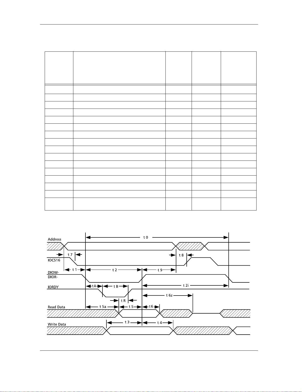
ATA Bus Interface and ATA Commands
Table 6-5
Table 6-5 PIO Host Interface Timing
Table 6-5 Table 6-5
SYMBOL
SYMBOL DESCRIPTION
SYMBOLSYMBOL
t0
t0 Cycle Time
t0t0
DESCRIPTION MIN/MAX
DESCRIPTIONDESCRIPTION
Cycle Time min
Cycle TimeCycle Time
MIN/MAX
MIN/MAXMIN/MAX
min 120
minmin
(local bus)
(local bus)
(local bus)(local bus)
MODE 4
MODE 4
MODE 4MODE 4
1111
120 120
120120
t1 Address Valid to DIOW–/DIOR–Setup min 25 25
t2 DIOW–/DIOR– Pulsewidth (8- or 16-bit) min 70 70
t2i DIOW–/DIOR– Negated Pulsewidth min 25 25
t3 DIOW–Data Setup min 20 20
t4 DIOW– Data Hold min 10 10
t5 DIOR– Data Setup min 20 20
t5a DIOR– to Data Valid max — —
t6 DIOR– Data Hold min 5 5
t6z DIOR– Data Tristate max 30 30
t7 Address Valid to IOCS16– Assertion max N/A N/A
t8 Address Valid to IOSC16– Deassertion max N/A N/A
t9 DIOW–/DIOR– to Address Valid Hold min 10 10
tA IORDY Setup Time min 35 35
tB IORDY Pulse Width max 1250 1250
tR Read Data Valid to IORDY active
min 0 0
(if IORDY is initially low after tA)
1. ATA Mode 4 timing is listed for reference only.
QUANTUM
QUANTUM
QUANTUMQUANTUM
Quantum
Quantum
Quantum Quantum
Fireball Plus
Fireball Plus
Fireball Plus Fireball Plus
AS
AS
ASAS
AT
AT
ATAT
120
120120
Figure 6-1
Figure 6-1 PIO Interface Timing
Figure 6-1 Figure 6-1
6-10 Quantum Fireball Plus AS 10.2/20.5/30.0/40.0/60.0 GB AT
Page 73

ATA Bus Interface and ATA Commands
6.4.2.2
6.4.2.2 Multiword DMA Transfer Mo de
6.4.2.26.4.2.2
Multiword DMA Transfer Mode
Multiword DMA Transfer ModeMul tiwo rd DMA Transfer Mode
The multiword DMA host interface timing shown in Table 6-6 is in reference to
signals at 0.8 volts and 2.0 volts. All times are in nanoseconds, unless otherwise
noted. Figure 6-2 provides a timing diagram.
Table 6-6
Table 6-6
Table 6-6 Table 6-6
SYMBOL
SYMBOL DESCRIPTION
SYMBOLSYMBOL
t0
t0 Cycle Time
t0t0
Multiword DMA Host Interface Timing
DESCRIPTION MIN/MAX
DESCRIPTIONDESCRIPTION
Cycle Time min
Cycle TimeCycle Time
MIN/MAX
MIN/MAXMIN/MAX
min
minmin
MODE 2
MODE 2
MODE 2MODE 2
(local bus)
(local bus)
(local bus)(local bus)
120 120
tD DIOR–/DIOW– Pulsewidth min 70 70
tE DIOR– to Data Vali d max – –
tF DIOR– Data Hold min 5 5
tFz DIOR– Data Tris tate
2
max 20 20
tG DIOW– Data Setu p min 20 20
tH DIOW– Data Hold min 10 10
tI DMACK to DIOR–/DIOW– Setup min 0 0
tJ DIOR–/DIOW– to DMACK– Hold min 5 5
tK DIOR–/DIOW– Negated Pulsewidth min 25 25
tL DIOR–/DIOW– to DMARQ Delay max 35 35
tz DMACK– Data Tristate
3
max 25 25
1. ATA Mode 2 timing is listed for reference only.
2. The Quantum Firebal l Plus AS 10.2/20.5/30 .0/40.0/60.0 GB AT d rive tristates
after each word transferred.
3. Symbol tz only applies on the last tristate at the end of a multiword DMA transfer
cycle.
Quantum
Quantum
Quantum Quantum
1111
Fireball Plus
Fireball Plus
Fireball Plus Fireball Plus
AS
AS
ASAS
AT
AT
ATAT
Figure 6-2
Figure 6-2 Multiword DMA Bus Interface Timing
Figure 6-2 Fig ure 6-2
Quantum Fireball Plus AS 10.2/20.5/30.0/40.0/60.0 GB AT 6-11
Page 74

ATA Bus Interface and ATA Commands
Table 6-7 contains the values for the timings for each of the Ultra DMA modes. All
timing measurement switching points (low to high and high to low) shall be taken
at 1.5V. Table 6-8 contains descriptions and comments for each of the timing values
in Table 6-7.
Table 6-7
Name
Name
NameName
Table 6-7
Table 6-7 Table 6-7
Mode 0
Mode 0
Mode 0Mode 0
(ns)
(ns)
(ns)(ns)
Min
Min Max
Max Min
MinMin
MaxMax
Ultra DMA Data Transfer Timing Requirements
Mode 1
Mode 1
Mode 1Mode 1
(ns)
(ns)
(ns)(ns)
Min Max
Max Min
MinMin
MaxMax
Mode 2
Mode 2
Mode 2Mode 2
(ins)
(ins)
(ins)(ins)
Min Max
Max Min
MinMin
MaxMax
Mode 3
Mode 3
Mode 3Mode 3
(ns)
(ns)
(ns)(ns)
Min Max
Max Min
MinMin
MaxMax
Mode 4
Mode 4
Mode 4Mode 4
(ns)
(ns)
(ns)(ns)
Min Max
Max Min
MinMin
MaxMax
Mode 5
Mode 5
Mode 5Mode 5
(ns)
(ns)
(ns)(ns)
Min Max
Max
MinMin
MaxMax
Measurement
Measurement
Measurement Measurement
Location
Location
LocationLocation
t
2CYCTYP
t
CYC
t
2CYC
t
DS
t
DH
t
DVS
t
DVH
t
CS
t
CH
t
CVS
t
CVH
t
ZFS
t
DZFS
t
FS
t
LI
t
MLI
t
UI
t
AZ
t
ZAH
t
ZAD
t
ENV
t
RFS
t
RP
t
IORDYZ
t
ZIORDY
t
ACK
t
SS
240160120906040Sender
1127354392516.8Recipient
230153115865738Sender
15.0 10.0 7.0 7.0 5.0 4.0 Recipient
5.0 5.0 5.0 5.0 5.0 4.6 Recipient
70.0 48.0 31.0 20.0 6.7 4.8 Sender
6.2 6.2 6.2 6.2 6.2 4.8 Sender
15.0 10.0 7.0 7.0 5.0 5.0 Device
5.0 5.0 5.0 5.0 5.0 5.0 Device
70.0 48.0 31.0 20.0 6.7 10.0 Host
6.2 6.2 6.2 6.2 6.2 10.0 Host
0000035Device
70.0 48.0 31.0 20.0 6.7 25 Sender
230 200 170 130 120 90 Device
01500150015001000100075Note 2
20 20 20 20 20 20 Host
000000Host
10 10 10 10 10 10 Note 3
20 20 20 20 20 20 Host
000000Device
20 70 20 70 20 70 20 55 20 55 20 50 Host
75 70 60 60 60 50 Sender
160 125 100 100 100 85 Recipient
20 20 20 20 20 20 Device
000000Device
20 20 20 20 20 20 Host
50 50 50 50 50 50 Sender
6-12 Quantum Fireball Plus AS 10.2/20.5/30.0/40.0/60.0 GB AT
Page 75

ATA Bus Interface and ATA Commands
Notes:
Notes:
Notes:Notes:
1. All signal transitio ns for a tim ing para meter will be measu red at the c onnector
specified in the measured location column. For example, in the case of t
both STROBE and DMARDY- transitions are measured at the sender
connector.
RFS
,
2. The parameter t
shall be measured at the connector of the sender or
LI
recipient that is responding to an incoming transition from the recipient or
sender respectively. Both the incoming signal and the outgoing response
will be measured at the same connector.
3. The parameter t
will be measured at the connector of the sender or
AZ
recipient that is releasing the bus.
Table 6-8
Table 6-8 Ultra DMA Data Burst Timing Descriptions
Table 6-8 Table 6-8
Name
Name Comment
NameName
t
2CYCTYP
t
CYC
t
2CYC
t
DS
t
DH
t
DVS
t
DVH
t
CS
t
CH
t
CVS
t
CVH
t
ZFS
t
DZFS
t
FS
t
LI
t
MLI
t
UI
t
AZ
t
ZAH
t
ZAD
t
ENV
t
RFS
t
RP
t
IORDYZ
Typical sustained average two cycle time
Cycle time allowing for asymmetry and clock variations (f rom STROBE ed ge to STROBE
edge)
Two cycle time allowing for clock variations (from rising edge to next rising edge or
from falling edge to next falling edge of STROBE)
Data setup time at recipient (from data valid until STROBE edge) (see notes 2,5)
Data hold time at recipient (from STROBE edge until data may become invalid) (see
note 2,5)
Data valid setup time at sender (from data valid until STROBE edge) (see note 3)
Data valid hold time at sender (from STROBE edge until data may become invalid) (see
note 3)
CRC word setup time at device (see note 2)
CRC word hold time device (see note 2)
CRC word valid setup time at host (from CRC va lid until DMACK- negation) (see note 3)
CRC word valid hold time at sender (from DMACK- negation until CRC may become
invalid) (see note 3)
Time from STROBE outpu t released -to-d riving until t he f irst transition of critical timing.
Time from data output released-to-driving until the first transition of critical timing.
First STROBE time (for device to first negate DSTROBE from STOP during a data in
burst)
Limited interlock time (see note 1)
Interlock time with minimum (see note 1)
Unlimited interlock time (see note 1)
Maximum time allowed for output drivers to release (from asserted or negated)
Minimum delay time required for output
drivers to assert or negate (from released)
Envelope time (from DMACK- to STOP and HDMARDY- during data in burst initiation
and from DMACK to STOP during data out burst initiation)
Ready-to-final-STROBE time (n o S TROBE ed ges shall be sent this long after negation of
DMARDY-)
Ready-to-pause time (that recipient shall wait to pause after negating DMARDY-)
Maximum time before releasing IORDY
Comment
Comment Comment
Quantum Fireball Plus AS 10.2/20.5/30.0/40.0/60.0 GB AT 6-13
Page 76

ATA Bus Interface and ATA Commands
t
ZIORDY
t
ACK
t
SS
Minimum time before driving IORDY (see note 4)
Setup and hold times for DMACK- (before assertion or negation)
Time from STROBE edge to negation of DMARQ or assertion of STOP (when sender
terminates a burst)
Notes:
Notes:
Notes:Notes:
1. The parameters t
UI
, t
and tLI indicate sender-to-recipient or recipient-to-
MLI
sender interlocks, i.e ., one agent (eit her sender or recipient ) is waiting for th e
other agent to respond with a signal before proceeding. t
interlock that has no maxi mum time value. t
a defined minimum. t
is a limited time-out that has a defined maximum.
LI
is a limite d time- out th at has
MLI
2. 80-conductor cabling will be required in order to meet setup (t
and hold (t
3. Timing for t
, tCH) times in modes greater than 2.
DH
, t
, t
DVS
DVH
CVS
and t
will be met for lumped capacitive
CVH
is an unlimited
UI
, tCS)
DS
loads of 15 and 40 pf at the connector where the Data and STROBE
signals have the same capacitive load value. Due to reflections on the
cable, these timing measurements are not valid in a normally functioning
system.
4. For all modes the parameter t
ZIORDY
may be greater than t
due to the
ENV
fact that the host has a pull up on IORDY- giving it a known state when
released.
5. The parameters t
, and tDH for mode 5 are de fined for a r ecipi ent a t the
DS
end of the cable o n ly i n a confi gurati on with o ne de vice a t the end of t he
cable.
Figures 6-3 through 6-12 define the timings associated with all phases of Ultra DMA
bursts.
6-14 Quantum Fireball Plus AS 10.2/20.5/30.0/40.0/60.0 GB AT
Page 77

DMARQ
(device)
DMACK-
(host)
STOP
(host)
HDMARDY-
(host)
DSTROBE
(device)
DD(15:0)
Tui
Tack
Tack
Tziordy
Taz
Tenv
Tenv
ATA Bus Interface and ATA Commands
Tfs
Tfs
Tdvs
Tzad
Tzad
Tdvh
Tack
DA0, DA1, DA2,
CS0-, CS1-
Figure 6-3
Figure 6-3 Initiating a Data In Burst
Figure 6-3 Fig ure 6-3
T2cyc
Tcyc Tcyc
T2cyc
Tdvs
DSTROBE
at device
Tdvh
DD(15:0)
at device
DSTROBE
at host
DD(15:0)
Note:
Note: DD(15:0) and DSTROBE signals are shown at both the host and
Note:Note:
Tdh
Figure 6-4
Figure 6-4 Sustained Data In Burst
Figure 6-4 Fig ure 6-4
Tds Tdh Tds
Tdvh
Tdvs
Tdvh
Tdh
the device to emphasize that cable settling time as well as cable
propagation delay shall not allow the data signals to be considered
stable at the host until well after they are driven by the device.
Quantum Fireball Plus AS 10.2/20.5/30.0/40.0/60.0 GB AT 6-15
Page 78

ATA Bus Interface and ATA Commands
DMARQ
(device)
DMACK-
(host)
STOP
(host)
HDMARDY
(host)
DSTROBE
(device)
DD(15:0)
(device)
DMARQ
(device)
DMACK-
(host)
STOP
(host)
HDMARDY-
(host)
DSTROBE
(device)
Trp
Tsr
Trfs
Figure 6-5
Figure 6-5 Host Pausing a Data In Burst
Figure 6-5 Figure 6-5
Note:
Note: The host knows the burst is fully paused Trp ns after
Note:Note:
HDMARDY- is negated and may then assert STOP to
terminate the burst. Tsr timing need not be met for an
asynchronous pause.
Tdvs
Tmli
Tack
Tack
Tiordyz
Tss
Tli
Tli
Tli
Tzah
Taz
Tdvh
DD(15:0)
DA0, DA1, DA2,
CS0-, CS1-
Figure 6-6
Figure 6-6
Figure 6-6 Fig ure 6-6
Device Terminating a Data In Burst
6-16 Quantum Fireball Plus AS 10.2/20.5/30.0/40.0/60.0 GB AT
CRC
Tack
Page 79

DMARQ
(device)
DMACK-
(host)
STOP
(host)
HDMARDY-
(host)
DSTROBE
(device)
DD(15:0)
Trfs
Trp
Tli
Tli
Taz
Tzah
ATA Bus Interface and ATA Commands
Tmli
Tmli
Tdvs
Tack
Tack
Tiordyz
Tdvh
CRC
DA0, DA1, DA2,
CS0-, CS1-
DMARQ
(device)
DMACK-
(host)
STOP
(host)
DDMARDY-
(device)
HSTROBE
(host)
DD(15:0)
(host)
DA0, DA1, DA2,
CS0-, CS1-
Tack
Figure 6-7
Figure 6-7 Host Terminating a Data In Burst
Figure 6-7 Figure 6-7
Tui
Tack Tenv
Tziordy
Tack
Tack
Tli
Tui
Tdvs
Tdvh
Figure 6-8
Figure 6-8 Initiating a Data Out Burst
Figure 6-8 Fig ure 6-8
Quantum Fireball Plus AS 10.2/20.5/30.0/40.0/60.0 GB AT 6-17
Page 80

ATA Bus Interface and ATA Commands
Tcyc Tcyc
HSTROBE
at host
Tdvh
DD(15:0)
at host
T2cyc
Tdvs Tdvs
Tdvh
T2cyc
Tdvh
HSTROBE
at device
DD(15:0)
at device
Note:
Note: DD(15:0) and HSTROBE signals are shown at both the device
Note:Note:
DMARQ
(device)
DMACK-
(host)
STOP
(host)
DDMARDY-
(device)
Tdh
Figure 6-9
Figure 6-9 Sustained Data Out Burst
Figure 6-9 Fig ure 6-9
Tds Tdh
Tds
Tdh
and the host to emphasize that cable settling time as well as
cable propagation delay shall not allow the data signals to be
considered stable at the device until well after they are driven
by the host.
Trp
Tsr
Trfs
HSTROBE
(host)
DD(15:0)
(host)
Figure 6-10
Figure 6-10
Figure 6-10 Figure 6-10
Note:
Note: The device knows the burst is fully paused Trp ns after
Note:Note:
Device Pausing a Data Out Burst
DDMARDY- is negated and may then negate DMARQ to
terminate the burst. Tsr timing need not be met for an
asynchronous pause.
6-18 Quantum Fireball Plus AS 10.2/20.5/30.0/40.0/60.0 GB AT
Page 81

ATA Bus Interface and ATA Commands
DMARQ
(device)
DMACK-
(host)
STOP
(host)
DDMARDY-
(device)
HSTROBE
(host)
DD(15:0)
(host)
DA0, DA1, DA2,
CS0-, CS1-
Tss
Tli
Tmli
Tack
Tli
Tli
Tdvs
CRC
Tiordyz
Tack
Tdvh
Tack
Figure 6-11
Figure 6-11 Host Terminating a Data Out Burst
Figure 6-11 Figure 6-11
Quantum Fireball Plus AS 10.2/20.5/30.0/40.0/60.0 GB AT 6-19
Page 82
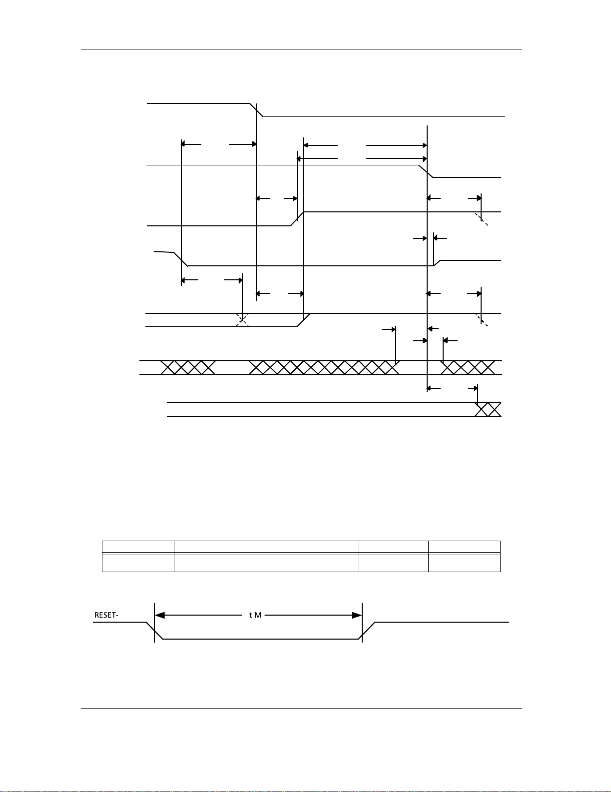
ATA Bus Interface and ATA Commands
DMARQ
(device)
DMACK-
(host)
TmliTrp
Tmli
STOP
(host)
DDMARDY-
(device)
Trfs
HSTROBE
(host)
DD(15:0)
(host)
DA0, DA1, DA2,
CS0-, CS1-
Figure 6-12
Figure 6-12 Device Terminating a Data out Burst
Figure 6-12 Figu re 6-12
6.4.2.3
6.4.2.3 Host Interface RESET Timing
6.4.2.36.4.2.3
Host Interface RESET Timing
Host Interface RESET TimingHost Interface RESET Timing
The host interface RESET timing shown in Table 6-9 is in reference to signals at 0.8
volts and 2.0 vol t s. Al l t im e s a re in n ano sec o n ds, unless otherwise note d. F igu re 6 13 provides a timing diagram.
Tli
Tli
Tack
Tiordyz
Tack
Tdvs
Tdvh
CRC
Tack
Table 6-9
Table 6-9
Table 6-9 Tab le 6-9
Host Interface RESET Timing
SYMBOL DESCRIPTION MINIMUM MAXIMUM
tM
RESET– Pulse width
Figure 6-13
Figure 6-13 Host Interface RESET Timing
Figure 6-13 Figure 6-13
25 —
6-20 Quantum Fireball Plus AS 10.2/20.5/30.0/40.0/60.0 GB AT
Page 83
6.5
6.5 REGISTER ADDRESS DECODING
6.56.5
REGISTER ADDRESS DECODING
REGISTER ADDRESS DECODINGREGISTER ADDRESS DECODING
The host addresses the drive by using programmed I/O. Host address lines A0–A2,
chip-select CS1FX– and CS3FX–, and IOR– and IOW– address the disk registers.
Host address lines A3–A9 generate the two chip-select signals, CS1FX– and
CS3FX–.
• Chip Select CS1FX– accesses the eight Command Block Registers.
• Chip Select CS3FX– is valid during 8-bit transfers to or from the
Alternate Status Register.
The drive selects the primary or secondary command block addresses by setting
Address bit A7.
Data bus lines 8–15 are valid only when IOCS16– is active and the drive is
transferring data. The drive transfers ECC information only on data bus lines 0–7.
Data bus lines 8–15 are invalid during transfers of ECC information.
I/O to or from the drive occurs over an I/O port that routes input or output data to
or from selected registers, by using the following encoded signals from the host:
CS1FX–, CS3FX–, DA2, DA1, DA0, DIOR–, and DIOW–. The host writes to the
Command Block Registers when transmitting commands to the drive, and to the
Control Block Registers when transmitting control, like a software reset. Table 6-10
lists the selection addresses for these registers.
ATA Bus Interface and ATA Commands
Table 6-10
Table 6-10
Table 6-10 Table 6-10
FUNCTION
FUNCTION HOST SIGNALS
FUNCTIONFUNCTION
CONTROL BLOCK REGISTERS
CONTROL BLOCK REGISTERS CS1FX–
CONTROL BLOCK REGISTERSCONTROL BLOCK REGISTERS
READ (DIOR–)
READ (DIOR–) WRITE (DIOW–)
READ (DIOR–)READ (DIO R–)
Data Bus High
Data Bus High
Data Bus High Data Bus High
Impedance
Impedance
ImpedanceImpedance
Data Bus High Impedance Not Used N A
I/O Port Functions and Selection Addresses
HOST SIGNALS
HOST SIGNALSHOST SIGNALS
WRITE (DIOW–)
WRITE (DIOW–)WRITE (DIOW–)
Not Used
Not Used NNNN
Not UsedNot Used
CS1FX– CS3FX–
CS1FX–CS1FX–
1111
CS3FX– DA2
CS3FX–CS3FX–
NNNNX
3
DA2 DA1
DA2DA2
X
XX
0XX
2222
DA1 DA0
DA1DA1
XXXXX
Data Bus High Impedance Not Used N A 1 0 X
Alternate Status Device Control N A 1 1 0
Drive Ad dress Not Used N A 1 1 1
COMMAND BLOCK REGISTERS
COMMAND BLOCK REGISTERS
COMMAND BLOCK REGISTERSCOMMAND BLOCK REGISTERS
READ (DIOR–)
READ (DIOR–) WRITE (DIOW–)
READ (DIOR–)READ (DIO R–)
WRITE (DIOW–)
WRITE (DIOW–)WRITE (DIOW–)
Data Port Data Por t A N 0 0 0
Error Register Features A N 0 0 1
Sector Count Sector Count A N 0 1 0
Sector Number
LBA Bits 0–7
Cylinder Low
LBA Bits 8–15
Cylinder High
LBA Bits 16–23
4
5
4
5
4
5
Sector Number A N 0 1 1
LBA Bits 0–7 A N 0 1 1
Cylinder Low A N 1 0 0
LBA Bits 8–15 A N 1 0 0
Cylinder High A N 1 0 1
LBA Bits 16–23 A N 1 0 1
DA0
DA0DA0
X
XX
Quantum Fireball Plus AS 10.2/20.5/30.0/40.0/60.0 GB AT 6-21
Page 84

ATA Bus Interface and ATA Commands
FUNCTION
FUNCTION HOST SIGNALS
FUNCTIONFUNCTION
Drive/Head
LBA Bits 24–27
Status Command A N 1 1 1
Invalid Address Invalid Address A A X X X
1. N = signal deasserted
2. X = signal either asserted or deasserted
3. A = signal asserted
4. Mapping of registers in CHS mode
5. Mapping of registers in LBA mode
4
5
After power on or following a reset, the drive ini tializes the Command Block
Registers to the values shown in Table 6-11.
Drive/Head A N 1 1 0
LBA Bits 24–27 A N 1 1 0
HOST SIGNALS
HOST SIGNALSHOST SIGNALS
Table 6-11
Table 6-11
Table 6-11 Table 6-11
6.6
6.6 REGISTER DESCRIPTIONS
6.66.6
6.6.1
6.6.1 Control Block Registers
6.6.16.6.1
6.6.1.1
6.6.1.1 Alternate Status Register
6.6.1.16.6.1.1
REGISTER DESCRIPTIONS
REGISTER DESCRIPTIONSREGISTER DESCRIPTIONS
The Quantum Fireball Plus AS 10.2/20.5/30.0/40.0/60.0 GB AT hard disk drives
emulate the ATA Command and Control Block Registers. Functional descriptions
of these registers are given in the next two sections.
Control Block Registers
Control Block RegistersControl Block Registers
Alternate Status Register
Alternate Status RegisterAlternate Status Register
The Alternate Status Register contains the same information as the Status Register
in the command block. Reading the Alternate Status Register does not imply the
acknowledgment of an interrupt by the ho st or clear a pending interrupt. See the
description of the Status Register in section 6.6.2.8 for definitions of bits in this
register.
Command Block Register Initial Values
Error Register 01
Sector Count Register 01
Sector Number Register 01
Cylinder Low Register 00
Cylinder High Register 00
Drive/Head Register 00
REGISTER
REGISTER VALUE
REGISTERREGISTER
VALUE
VALUEVALUE
6-22 Quantum Fireball Plus AS 10.2/20.5/30.0/40.0/60.0 GB AT
Page 85

6.6.1.2
6.6.1.2 Device Control Register
6.6.1.26.6.1.2
Device Control Register
Device Control RegisterDevice Control Register
This write-only register contains two control bits, as shown in Table 6-12.
Table 6-12
Table 6-12
Table 6-12 Table 6-12
BIT
BIT MNEMONIC
BITBIT
MNEMONIC DESCRIPTION
MNEMONICMNEMONIC
7Reserved –
6Reserved –
5Reserved –
4Reserved –
31 Always 1
2SRST
1nIEN
1
2
00 Always 0
1. SRST = Host Software Reset bit. When the host sets this bit, the drive
is reset. When two drives are daisy-chained on the interface, this bit
resets both drives simulta ne ous ly .
ATA Bus Interface and ATA Commands
Device Control Register Bits
DESCRIPTION
DESCRIPTIONDESCRIPTION
Host software reset bit
Drive interrupt enable bit
2. nIEN = Drive Interrupt Enable bit. When nIEN eq uals 0 or the host
has selected the drive, the drive enables the host interrupt signal
INTRQ through a tristate buffer to the host. Whe n nIEN equals 1 o r
the drive is not selected, the host interrupt signal INTRQ is in a highimpedance state, regardless of the presence or absence of a pending
interrupt.
Quantum Fireball Plus AS 10.2/20.5/30.0/40.0/60.0 GB AT 6-23
Page 86

ATA Bus Interface and ATA Commands
6.6.1.3
6.6.1.3 Drive Address Register
6.6.1.36.6.1.3
7HiZ
6nWTG
5nHS3
4nHS2–
3nHS1–
2 nHS0 Head Address lsb
1nDS1
0nDS0Drive 0 Select bit
1. HiZ = High Impedance bit. When the host reads the register, this bit will be in a high
2. nWTG = Write G ate bit. When a wri te operation to th e drive is in progr ess, nWTG
3. nHS0–nHS3 = Head Address bits. These bits are equivalent to the one’s complement
4. nDS0–nDS1 = Drive Sel ect bits . When d ri ve 1 is se lect ed, nD S1 eq uals 0 . Wh en driv e
Drive Address Register
Drive Address RegisterDrive Address Register
The Drive Address Regist er returns the head-select add resses for the drive curre ntly
selected. Table 6-13 shows the Drive Address bits.
Table 6-13
Table 6-13
Table 6-13 Table 6-13
BIT
BIT MNEMONIC
BITBIT
impedance state.
equals 0.
of the binary-coded address of the head currently selected.
0 is selected, nDS0 equals 0.
Drive Address Register Bits
MNEMONIC DESCRIPTION
MNEMONICMNEMONIC
1
2
3
4
DESCRIPTION
DESCRIPTIONDESCRIPTION
High Impedance bit
Write Gate bit
Head Address msb
Drive 1 Select bit
6.6.2
6.6.2 Command Block Registers
6.6.26.6.2
6.6.2.1
6.6.2.1 Data Port Register
6.6.2.16.6.2.1
6.6.2.2
6.6.2.2 Error Register
6.6.2.26.6.2.2
Command Block Registers
Command Block RegistersCommand Block Registers
Data Port Register
Data Port RegisterData Port Register
All data transferr ed between th e device data buffer and t he host pa sses thro ugh the
Data Port Register. The host transfers the sector table to this register during
execution of the FORMAT TRACK command.
Error Register
Error RegisterError Regi st er
The Error Register contains status information about the last command executed by
the drive. The contents of this register are valid only when the Error bit (ERR) in
the Status Register is set to 1. The contents of the Error Register are also valid at
power on, and at the completion of the drive’s internal diagnostics, when the
register contains a status code. When t he error bit in the Sta tus Register is set to 1,
the host interprets the Error Register bits as shown in Table 6-14.
6-24 Quantum Fireball Plus AS 10.2/20.5/30.0/40.0/60.0 GB AT
Page 87

ATA Bus Interface and ATA Commands
Table 6-14
Table 6-14 Error Register Bits
Table 6-14 Table 6-14
MNEMONIC
MNEMONIC BIT
MNEMONICMNEMONIC
BIT DESCRIPTION
BITBIT
DESCRIPTION
DESCRIPTIONDESCRIPTION
#7
#6
#5
#4
#3
ABRT 2 Requested command aborted due to a drive status error, such as Not
Ready or Write Fault, or because the command code is invalid.
#1
#0
6.6.2.3
6.6.2.3 Sector Count Register
6.6.2.36.6.2.3
Sector Count Register
Sector Count RegisterSector Count Register
The Sector Count Register defines the number of sectors of data to be transferred
across the host bus for a subsequent command. If the v alue in thi s registe r is 0, the
sector count is 256 sectors. If the Sector Count Register command executes
successfully, the value in this register at command completion is 0. As the drive
transfers each se ctor, it decr ements the Sector Count Register to reflect t he number
of sectors remaining to be transferred. If the command’s execution is unsuccessful,
this register contains the number of sectors that must be transferred to complete the
original request.
When the drive executes an INITIALIZE DRIVE PARAMETE RS or Format Track
command, the value in this register defines the number of sectors per track.
6.6.2.4
6.6.2.4 Sector Number Register
6.6.2.46.6.2.4
Sector Number Register
Sector Number RegisterSector Number Register
The Sector Number Register contains the ID number of the first sector to be
accessed by a subsequent command. The secto r number is a value between one and
the maximum number of sectors per track. As the drive transfers each sector, it
increments the Sector Number Register. See the command descriptions in section
6.7 for information about the contents of the Sector Number Register after
successful or unsuccessful command completion.
In LBA mode, this register contains bits 0 to 7. At command completion, the host
updates this register to reflect the current LBA bits 0 to 7.
6.6.2.5
6.6.2.5 Cylinder Low Register
6.6.2.56.6.2.5
Cylinder Low Register
Cylinder Low RegisterCylinder Low Register
The Cylinder Low Register contains the eight lo w-order bits of the starti ng cylinder
address for any disk access. On multiple sector transfers that cross cylinder
boundaries, the drive updates this register when command execution is complete,
to reflect the current cylinder number. The host loads the least significant bits of the
cylinder address into the Cylinder Low Register.
In LBA mode, this register contains bits 8 to 15. At command completion, the drive
updates this register to reflect the current LBA bits 8 to 15.
Quantum Fireball Plus AS 10.2/20.5/30.0/40.0/60.0 GB AT 6-25
Page 88

ATA Bus Interface and ATA Commands
6.6.2.6
6.6.2.6 Cylinder High Register
6.6.2.66.6.2.6
Cylinder High Register
Cylinder High RegisterCylinder High Register
The Cylinder High Register contains the eight high-order bits of the starting
cylinder address for any disk access. On multiple sector transfers that cross cylinder
boundaries, the drive updates this register at the completion of command
execution, to reflect the current cylinder number. The hos t loads the most
significant bits of the cylinder address into the Cylinder High Register.
In LBA mode, this register contains bits 16 to 23. At command completion, the host
updates this register to reflect the current LBA bits 16 to 23.
6.6.2.7
6.6.2.7 Drive/Head Register
6.6.2.76.6.2.7
Drive/Head Register
Drive/Head RegisterDrive/Head Register
The Drive/Head Register contains the drive ID number and its head numbers. At
command completion this register is updated by the drive to reflect the current
head.
In LBA mode, this register contains bits 24 to 27. At command completion, the
drive updates this register to reflect the current LBA bits 24 to 27.
Table 6-15 shows the Drive/Head Register bits.
Table 6-15
Table 6-15
Table 6-15 Table 6-15
MNEMONIC
MNEMONIC BIT
MNEMONICMNEMONIC
Reserved 7
L6
BIT DESCRIPTION
BITBIT
1
2
Reserved 5 Always
DRV 4
HS3 3
3
4
Drive Head Register Bits
DESCRIPTION
DESCRIPTIONDESCRIPTION
Always
0
1
1
for CHS mode
for LBA mode
1
0
indicates the Master drive is selected
1
indicates the Slave drive is selected
Most significant Head Address bit in CHS mode
Bit 24 of the LBA Address in LBA mode
HS2 2 Head Address bit for CHS mode
Bit 25 of the LBA Address in LBA mode
HS1 1 Head Address bit for CHS mode
Bit 26 of the LBA Address in LBA mode
HS0 0 Least significant Head Address bit in CHS mode
Bit 27 of the LBA Address in LBA mode
1. Bits 5–7 define the sector size set in hardware (512 bytes).
2. Bit 6 is the binary encoded Address Mode Select. When bit 6 is set to 0,
addressing is by CHS mode. When bit 6 is set to 1, addressing is by LBA mode.
3. Bit 4 (DRV) contains the binary encoded drive select number. The Master is
the primary drive; the Slave is the secondary drive
4. In CHS mode , bi ts 3– 0 ( HS0 –HS 3) con ta in th e b ina ry enc ode d a ddr ess of the
selected head. At com mand complet ion, the ho st updates th ese bits to reflect
the address of t he head curre ntly se lect ed. In LBA mod e, bi ts 3 –0 (HS 0–HS3 )
contain bits 24–27 of the LBA Address. At command completion, the host
updates this register to reflect the current LBA bits 24 to 27.
6-26 Quantum Fireball Plus AS 10.2/20.5/30.0/40.0/60.0 GB AT
Page 89

6.6.2.8
6.6.2.8 Status Register
6.6.2.86.6.2.8
Status Register
Status RegisterStatus Register
The Status Register contains information about the status of the drive and the
controller. The driv e upda tes the conte nts o f th is re gister a t the complet ion of each
command. When the Busy bit is set (BSY=1), no other bits in the Command Block
Registers are valid. When the Busy bit is not set (BSY=0), the information in the
Status Register and Command Block Registers is valid.
When an interrupt is pending, the drive considers that the host has acknowledged
the interrupt when it rea ds the Sta tus Register. T herefore, whe never th e host reads
this register, the drive clears any pending interrupt. Table 6-16 defines the Status
Register bits.
ATA Bus Interface and ATA Commands
Table 6-16
Table 6-16
Table 6-16 Table 6-16
MNEMONIC
MNEMONIC BIT
MNEMONICMNEMONIC
BSY 7 Busy bit. Set by the controller logic of the drive whenever the
DRDY 6 Drive Ready bit. Indicates that the drive is ready to accept a
#5
#4
DRQ 3 Data Request bit. When set, this bit indicates that the drive is ready to
Obsolete 2
Obsolete 1
ERR 0 Error bit. When set, this bit indicates that the previous command
BIT DESCRIPTION
BITBIT
drive has access to and the host is locked out of the Command
Block Registers.
BSY is set under the following conditions:
• Within 400 ns after the deassertion of RESET- or after SRST is set in
the Device Control Register. Following a reset, BSY will be set for no
longer than 30 seconds.
• Within 400 ns of a host write to the Comm and Block R egisters with
a Read, READ LONG, READ BUFFER, SEEK, RECALIBRATE, INITIALIZE
DRIVE PARAMETERS, Read Verify, Identify Drive, or EXECUTE DRIVE
DIAGNOSTIC command.
• Within 5 µsec after the transfer of 512 bytes of data during the
execution of a Write, Format Track, or WRITE BUFFER command, or
512 bytes of data and the appropriate number of ECC bytes during
the execution of a WRITE LONG command.
When BSY=1, the host cannot write to a Command Block Register
and reading any Command Block Register returns the cont ents of th e
Status Register.
command. When an error occurs, this bit remains unchanged until
the host reads the Status Register, then again indicates that the drive
is ready. At power on, this bit should be cleared, and should remain
cleared until the drive is up t o speed and ready to ac cept a co mmand.
transfer a w ord or byte of data from the host to th e data port.
resulted in an error. The other bits in the Status Register and the bits
in the Error Register contain additional information about the cause
of the error.
Status Register Bits
DESCRIPTION
DESCRIPTIONDESCRIPTION
Note:
Note: The content of # bit is command dependent.
Note:Note:
Bits 2 and 1 are obsolete according to the ATA-4 specification.
Quantum Fireball Plus AS 10.2/20.5/30.0/40.0/60.0 GB AT 6-27
Page 90

ATA Bus Interface and ATA Commands
6.6.2.9
6.6.2.9 Command Register
6.6.2.96.6.2.9
Table 6-17
Table 6-17
Table 6-17 Table 6-17
Command Register
Command RegisterCommand Register
The host sends a command to the drive by means of an 8-bit code written to the
Command Register. As soon as the drive receives the command in its Command
Register, it begins execution of the command. Table 6-17 lists the hexadecimal
command codes and parameters for each executable command. The code F0h is
common to all of the extended comma nds. Each of these commands is disti nguished
by a unique subcode. For a de tai led des cri pti on of each com mand , s ee S ectio n 6. 7,
"COMMAND DESCRIPTIONS," found later in this chapter.
Quantum Fireball Plus AS 10.2/20.5/30.0/40.0/60.0 GB AT Command Codes
and Parameters
COMMAND
COMMAND PARAMETER
COMMANDCOMMAND
SC
SC
SCSC
Ex.
Ex.
NAME
NAME CODE
NAMENAME
RECALIBRATE 1Xh V
READ SECTORS 20hVVVVV
WRITE SECTORS 30hVVVVV
READ VERIFY SECTORS 40hVVVVV
SEEK 7Xh VVVV
EXECUTE DRIVE DIAGNOSTIC 90h
INITIALIZE DRIVE PARAMETERS 91h V V V
DOWNLOAD MICROCODE 92hVVVVV
SMART B0h V V
READ MULTIPLE C4hVVVVV
WRITE MULTIPLE C5hVVVVV
SET MULTIPLE MODE C6h V V
READ DMA C8hVVVVV
WRITE DMA CAhVVVVV
STANDBY IMMEDIATE E0h V
IDLE IMMEDIATE E1h V
STANDBY MODE (AUTO POWER-DOWN) E2h V V
IDLE MODE (AUTO POWER-DOWN) E3h V V
READ BUFFER E4h V
CHECK POWER MODE E5h V V
SLEEP MODE E6h V
FLUSH CACHE—optional cmnd. E7h V
WRITE BUFFER E8h V
IDENTIFY DRIVE ECh V
READ DEFECT LIST—extended cmnd. F0h O0h V V V
READ CONFIGURATION—extended cmnd. F0h O1h V V V
SET CONFIGURATION—extended cmnd. F0h FEh/
SCAN VERIFY—extended cmnd. F0h FCh V V V
GET SCAN VERIFY STATUS—extended cmnd. F 0h FDh V V V
READ NATIVE MAX ADDRESS F8
SET MAX ADDRESS F9 VVVV
CODE
CODECODE
Ex. Ex.
Sub
Sub
SubSub
Code
Code
CodeCode
FFh
PARAMETER
PARAMETERPARAMETER
SN
SN CY
SNSN
VVV
CY DS
CYCY
DS HD
DSDS
HD FR
HDHD
FR
FRFR
Note:
Note: The following information applies to Table 6-17:
Note:Note:
6-28 Quantum Fireball Plus AS 10.2/20.5/30.0/40.0/60.0 GB AT
Page 91

SC = Sector Count Register
SN = Sector Number Register
CY = Cylinder Low and High Registers
DS = Drive Select bit (Bit 4 of Drive/Head Register)
HD = 4 Head Select Bits (Bits 0–3 of Drive Head Register)
V = Must contain valid information for this command Head
FR = Features Register
6.7
6.7 COMMAND DESCRIPTIONS
6.76.7
COMMAND DESCRIPTIONS
COMMAND DESCRIPTIONSCOMMAND DESCRIPTIONS
The Quantum Fireball Plus AS hard disk drives support all standard ATA drive
commands. The drive decodes, then executes, commands l oaded into the Command
Block Register. In applications involving two hard drives, both drives receive all
commands. However, only the selected drive executes commands—with t he
exception of the EXECUTE DRIVE DIAGNOSTIC command, as explained below.
The procedure for executing a command on the selected drive is as follows:
1. Wait for the drive to indicate that it is no longer busy (BSY=0).
2. Activate the Interrupt Enable (–IEN) bit.
3. Wait for the drive to set RDY (RDY=1).
4. Load the required parameters into the Command Block Register.
5. Write the command code to the Command Register.
ATA Bus Interface and ATA Commands
Execution of the command begins as soon as the drive loads the Command Block
Register. The remainder of this section describes the function of each command.
The commands are listed in the same order they appear in Table 6-17.
6.7.1
6.7.1 Recalibrate
6.7.16.7.1
Features na
Sector Count na
Sector Number na
Cylinder Low na
Cylinder High na
Device/ Head obsnaobsDEVnaNanana
Command 1xh
Recalibrate
RecalibrateRecalibrate
COMMAND CODE – 1xh
DESCRIPTION – The RECALIBRATE command moves the read/write heads from
any location on the disk to cylinder 0. On receiving this command, the drive sets the
BSY bit and issues a seek command to cylinder 0 . The drive then waits for the seek
operation to complete, updates status, negates BSY, and generates an interrupt. If
the drive cannot seek to cylinder 0, it posts the message TRACK 0 NOT FOUND
(TK0NF).
INPUTS
Register
Register 77776
RegisterRegister
65
66
54
55
43
44
32
33
21
22
10
11
0
00
Quantum Fireball Plus AS 10.2/20.5/30.0/40.0/60.0 GB AT 6-29
Page 92
ATA Bus Interface and ATA Commands
ERROR OUTPUTS
Register
Register 77776
RegisterRegister
Error nananananaABRTTK0NFna
Sector Count na
Sector Number na
Cylinder Low na
Cylinder High
Device/ Head obs na obs DEV HEAD number or LBA
Status BSY DRDY na na DRQ na na ERR
6.7.2
6.7.2 Read Sectors
6.7.26.7.2
Read Sectors
Read SectorsRead Sectors
COMMAND CODE – 20h
DESCRIPTION – The READ sectors command reads from 1 to 256 sectors,
beginning at the specified sector. As specified in the command block register, a
sector count equal to 0 requests 256 sectors. When the drive accepts this command,
it sets BSY and begins execution of the command.
65
66
54
55
43
44
32
33
21
22
10
11
0
00
INPUTS
Register
Register 77776
RegisterRegister
Features na
Sector Count Sector count
Sector Number Sector count or LBA
Cylinder Low Cylinder low or LBA
Cylinder High Cylinder high or LBA
Device/ Head obs LBA obs DEV na Head Number or LBA
Command 20h
ERROR OUTPUTS
Register
Register 77776
RegisterRegister
Error na unc na IDNF na ABRT na na
Sector Count na
Sector Number na
Cylinder Low na
Cylinder High
Device/ Head obs na obs DEV HEAD number or LBA
Status BSY DRDY DF na DRQ na na ERR
65
66
65
66
54
55
54
55
43
44
43
44
32
33
32
33
21
22
21
22
10
11
10
11
0
00
0
00
6-30 Quantum Fireball Plus AS 10.2/20.5/30.0/40.0/60.0 GB AT
Page 93

ATA Bus Interface and ATA Commands
6.7.3
6.7.3 Write Sectors
6.7.36.7.3
Features na
Sector Count Sector count
Sector Number Sector count or LBA
Cylinder Low Cylinder low or LBA
Cylinder High Cylinder high or LBA
Device/ Head obs LBA obs DEV na Head Number or LBA
Command 30h
Write Sectors
Write SectorsWrite Sectors
COMMAND CODE – 30h
DESCRIPTION – The WRITE sectors command reads from 1 to 256 sectors,
beginning at the specified sector. As specified in the command block register, a
sector count equal to 0 requests 256 sectors. When the drive accepts this command,
it sets DRQ and waits for the host to fill the sector buffer with data to be written to
the drive. The drive does not generate an interrupt to start the first buffer-fill
operation. Once the buffer is full, the drive clears DRQ, sets BSY, and begins
execution of the command.
INPUTS
Register
Register 77776
RegisterRegister
65
66
54
55
43
44
32
33
21
22
10
11
0
00
ERROR OUTPUTS
Register
Register 77776
RegisterRegister
Error na unc na IDNF na ABRT na na
Sector Count na
Sector Number na
Cylinder Low na
Cylinder High
Device/ Head obs na obs DEV HEAD number or LBA
Status BSY DRDY DF na DRQ na na ERR
65
66
54
55
43
44
32
33
21
22
10
11
0
00
Quantum Fireball Plus AS 10.2/20.5/30.0/40.0/60.0 GB AT 6-31
Page 94

ATA Bus Interface and ATA Commands
6.7.4
6.7.4 Read Verify Sectors
6.7.46.7.4
Features na
Sector Count Sector count
Sector Number Sector Number or LBA
Cylinder Low Cylinder low or LBA
Cylinder High Cylinder high or LBA
Device/ Head obs LBA obs DEV na Head Number or LBA
Command 40h
Read Verify Sectors
Read Verify SectorsRead Verify Sectors
COMMAND CODE – 40h
DESCRIPTION – The READ VERIFY sectors executes similarly to the READ
SECTORS command but without ever generating an interrupt (DRQ) so that no
data is transferred to th e ho st .
INPUTS
Register
Register 77776
RegisterRegister
65
66
54
55
43
44
32
33
21
22
10
11
0
00
ERROR OUTPUTS
Register
Register 77776
RegisterRegister
Error na UNC na IDNF na ABRT na obs
Sector Count na
Sector Number Sector Number or LBA
Cylinder Low Cylinder low or LBA
Cylinder High Cylinder high or LBA
Device/ Head obs Na obs DEV HEAD number or LBA
Status BSY DRDY DF na DRQ na na ERR
65
66
54
55
43
44
32
33
21
22
10
11
0
00
6-32 Quantum Fireball Plus AS 10.2/20.5/30.0/40.0/60.0 GB AT
Page 95

6.7.5
6.7.5 Seek
6.7.56.7.5
Seek
SeekSeek
COMMAND CODE – 70h
DESCRIPTION – The SEEK command causes the actuator to seek to the LBA or
Cylinder location indicated in the LBA Registers or Cylinder Registers.
When the drive receives this command in its Command Block Registers, it performs
the following functions:
The drive does not wait for the seek to complete before it sends an interrupt. If the
BSY bit is not set in the Status Register, the drive can accept and queue subsequent
commands while performing the seek. If the Cylinder registers contain an illegal
cylinder, the drive sets the ERR bit in the Status Register and the IDNF bit in the
Error Register.
INPUTS
ATA Bus Interface and ATA Commands
1. Sets BSY
2. Initiates the seek operation
3. Resets BSY
4. Sets the Drive Seek Complete (DSC) b it in the Status Register
Register
Register 77776
RegisterRegister
Features na
Sector Count Sector count
Sector Number Sector Number or LBA
Cylinder Low Cylinder low or LBA
Cylinder High Cylinder high or LBA
Device/ Head obs LBA obs DEV na Head Number or LBA
Command 70h
OUTPUTS
Register
Register 77776
RegisterRegister
Error na UNC na IDNF na ABRT na obs
Sector Count na
Sector Number Sector Number or LBA
Cylinder Low Cylinder low or LBA
Cylinder High Cylinder high or LBA
Device/ Head obs Na obs DEV HEAD number or LBA
Status BSY DRDY DF DSC DRQ na na ERR
65
66
65
66
54
55
54
55
43
44
43
44
32
33
32
33
21
22
21
22
10
11
10
11
0
00
0
00
Quantum Fireball Plus AS 10.2/20.5/30.0/40.0/60.0 GB AT 6-33
Page 96

ATA Bus Interface and ATA Commands
6.7.6
6.7.6 Execute Drive Diagnostics
6.7.66.7.6
Execute Drive Diagnostics
Execute Drive DiagnosticsExecute Drive Diagnostics
COMMAND CODE – 90h
DESCRIPTION – The EXECUTE DRIVE DIAGNOSTIC command performs the
internal diagnostic s te st imp leme nted in the driv e. Dri ve 0 se ts BSY withi n 400 ns
of receiving the command.
If drive 1 is present:
• Both drives execute diagnostics.
• Drive 0 waits up to six seconds for drive 1 to assert PDIAG-.
• If drive 1 does not assert PDIAG- to indicate a failure, drive 0 appends
80h with its own diagnostics status.
• If the host detects a drive 1 diagnostic failure when reading drive 0
status, it sets the DRV bit, then reads the drive 1 status.
If drive 1 is not present:
• Drive 0 reports only its own diagnostic results.
• Drives 0 clears BSY and generates an interrupt.
The diagnostic code written to the error is a unique 8 bit code. Table 6-18 list the
diagnostics codes.
Table 6-18
Table 6-18
Table 6-18 Table 6-18
Diagnostic Code
Diagnostic Code Description
Diagnostic CodeDiagnostic Code
01h No error detected
02h Formatter Device Error
03h Sector Buffer error
04h ECC circuitry error
05h Controlling microprocessor error
81h Drive 1 failed, Drive 0 passed
80h,82h-FF Drive 0 failed, Drive 1 failed
Diagnostics Codes
Description
DescriptionDescription
6-34 Quantum Fireball Plus AS 10.2/20.5/30.0/40.0/60.0 GB AT
Page 97

ATA Bus Interface and ATA Commands
INPUTS
Register
Register 77776
RegisterRegister
65
66
54
55
43
44
32
33
21
22
10
11
Features na
Sector Count Sector count
Sector Number Sector Number or LBA
Cylinder Low Cylinder low or LBA
Cylinder High Cylinder high or LBA
Device/ Head obs LBA obs DEV na Head Number or LBA
Command 90h
OUTPUTS
Register
Register 77776
RegisterRegister
65
66
54
55
43
44
32
33
21
22
10
11
Error Diagnostic Code
Sector Count Signature
Sector Number Signature
Cylinder Low Signature
Cylinder High Signature
Device/ Head Signature
Status BSY DRDY DF na DRQ na na ERR
0
00
0
00
Quantum Fireball Plus AS 10.2/20.5/30.0/40.0/60.0 GB AT 6-35
Page 98
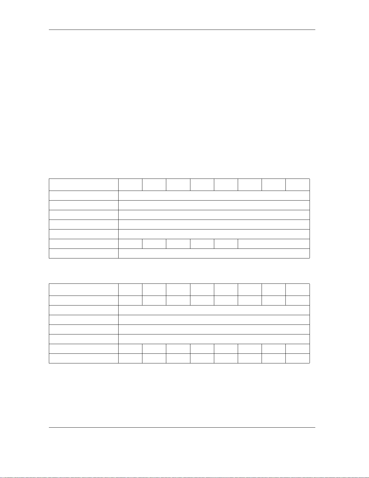
ATA Bus Interface and ATA Commands
6.7.7
6.7.7 INITIALIZE DRIVE P ARAMETERS
6.7.76.7.7
Features na
Sector Count Logical sectors per logical track
Sector Number na
Cylinder Low na
Cylinder High na
Device/ Head obs na obs DEV na Max head
Command 91h
INITIALIZE DRIVE PARAMETERS
INITIALIZE DRIVE PARAMETERSINITIALIZE DRIVE PARAMETERS
COMMAND CODE – 91h
DESCRIPTION – The INITIALIZE DRIVE PARAMETERS command enables the
host to set the logical number of heads and the logical number of sectors per track.
On receiving the command, the drive sets the BSY bit, saves the parameters, clears
the BSY, and generates an interrupt.
The only two register valu es used by thi s command are the Se ctor C ount register,
which specifies the number of sectors; and the Drive/Head register, which
specifies the number of hea ds, minus 1. Th e DRV bi t a ssigns these val ues to dri ve
0 or drive 1.
This command does not check the sector count and head values for validity. If these
values are invalid, th e dri ve wi ll not re port an err or until an other comma nd ca uses
an illegal access.
INPUTS
Register
Register 77776
RegisterRegister
65
66
54
55
43
44
32
33
21
22
10
11
0
00
OUTPUTS
Register
Register 77776
RegisterRegister
Error nananananaABRTnana
Sector Count na
Sector Number na
Cylinder Low na
Cylinder High na
Device/Head Obs na Obs DEV Na na na na
Status BSY na DF na DRQ na na ERR
6-36 Quantum Fireball Plus AS 10.2/20.5/30.0/40.0/60.0 GB AT
65
66
54
55
43
44
32
33
21
22
10
11
0
00
Page 99

6.7.8
6.7.8 Download Microcode
6.7.86.7.8
Sector Number Sector count (high order)
Download Mic rocode
Download Mic rocodeDownload Mic rocode
COMMAND CODE - 92h
TYPE - Optional
PROTOCOL - PIO data out
INPUTS - The head bits of the device/head register will always be set to zero. The
cylinder high and low registers will be set to zero. The sector number and the sector
count are used together as a 16-bit sector count value. The feature register specifies
the subcommand code.
Register
Register 77776
RegisterRegister
Features Subcommand code
Sector Count Sector count (low order)
Cylinder Low 00h
Cylinder High 00h
Device/Head 1 1D0000
Command 92h
65
66
54
55
43
44
ATA Bus Interface and ATA Commands
32
33
21
22
10
11
0
00
NORMAL OUTPUTS - None. required.
ERROR OUTPUTS - Aborted command if the device does not support this
command or did not accept the microcode data. Aborted error if subcommand code
is not a supported value.
Register
Register 77776
RegisterRegister
Error na
Sector Count na
Sector Number na
Cylinder Low na
Cylinder High na
Device/Head Obs na Obs DEV na na na na
Status BSY DRDY DF na DRQ na na ERR
PREREQUISITES - DRDY set equal to one.
DESCRIPTION - This command enables the host to alter the device’s microcode.
The data transferred using the DOWNLOAD MICROCODE command is vendor
specific.
All transfers will be an integer multiple of the sector size. The size of the data
transfer is determined by the contents of the Sector Number register and the Sector
Count register. The Sector Number register will be used to extend the Sector Count
register, to create a sixteen bit sector count value. The Sector Number register will
be the most significant eight bits and the Sector Count register will be the least
significant eight bits. A value of zero in both the Sector Number register and the
65
66
54
55
43
44
32
33
21
22
10
11
0
00
Quantum Fireball Plus AS 10.2/20.5/30.0/40.0/60.0 GB AT 6-37
Page 100
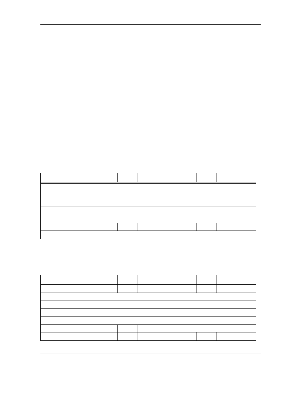
ATA Bus Interface and ATA Commands
Sector Count register will indicate no data is to transferred. This allows transfer
sizes from 0 bytes to 33, 553, 920 bytes in 512 byte increments.
The Features register will be used to determine the effect of the DOWNLOAD
MICROCODE sub command. The values for the Feature Register are:
01h — download is for immediate, temporary use
07h — save downloaded code for immediate and future use.
Either or both values may be supported. All other values are reserved.
6.7.9
6.7.9 SMART
6.7.96.7.9
SMART
SMARTSMART
SMART DISABLE OPERATIONS
COMMAND CODE - B0h
TYPE - Optional - SMART Feature set. If the SMART feature set is implemented,
this command shall be implemented.
PROTOCOL - Non-data command
INPUTS - The Features register shall be set to D9h. The Cylinder Low register sh all
be set to 4Fh. The Cylinder High register shall be set to C2h.
Register
Register 77776
RegisterRegister
Features D9h
Sector Count
Sector Numb er
Cylinder Low 4Fh
Cylinder High C2h
Device/Head 1 1 D
Command B0h
NORMAL OUTPUTS - None
ERROR OUTPUTS - If the device does not support this command, if SMART is not
enabled or if the values in th e Features, Cylinder Low o r Cylinder High register s are
invalid, an Aborted command error is posted.
Register
Register 77776
RegisterRegister
Error nananananaABRTnana
Sector Count na
Sector Number na
Cylinder Low na
Cylinder High na
Device/Head obs na obs DEV
Status BSY DRDY DF na DRQ na na ERR
65
66
65
66
54
55
54
55
43
44
43
44
32
33
32
33
21
22
21
22
10
11
10
11
0
00
0
00
6-38 Quantum Fireball Plus AS 10.2/20.5/30.0/40.0/60.0 GB AT
 Loading...