SE K630, V640 K660 Schematic
SEMC Troubleshooting Manual
ABOUT
K630 - V640 - K660
Troubleshooting Manual
K630 - V640 - K660
ABOUT TROUBLESHOOTING MEASUREME NT POINTS
1215-3608 rev. 1
APPENDIXCOMPONENT OVERVIEW FUNCTIONAL OVERVIEW
1 (96)

ABOUT
ABOUT Contents
SEMC Troubleshooting Manual
K630 - V640 - K660
General information
The purpose of this document is to provide enhanced technic al information for Sony Ericsson
repair technicians in order to assist during service, repair and troubleshooting operations on Sony
Ericsson mobile phones. It should be used as a c omplement to other repair instructions and tools
as notified by the local Sony Ericsson repre sentative.
To search for components throughout the entire document use the “search” function in Adobe
Acrobat Reader 7.0 (or later version) and enter the component name or other word. Use zoom to
enlarge.
For easier navigation of the document you can use the bookmarks that appear in the Bookmarks
tab on the left side of the Adobe Acrobat Reader window. Each bookmark jumps to a page in the
document.
Disclaimer
This document is Sony Ericsson confidential and should be t reated as confi dential in accordance
with the agreement with Sony Ericsson. This document is intended for use by authorized service
technicians only. Sony Ericsson is not to be held responsible for any damages or losses caused
intentionally or unintentionally due to unauthorise d use of the information in this document.
Revision History
Rev. Date Changes / Comments
1
06/20/2008 Initital revision.
ABOUT 2 Connectivity Connectivity 40
General Information 2
Contents 2 Imaging Top 42
TROUBLESHOOTING 3 Imaging Camera 44
Equipment List 3 Access Top 45
On/Off Problems 9 Access GMS & UMTS 46
Flash Problems 9 Access Bluetooth 47
Dead Phone Problems 10 Audio Top 48
Display Problems 11 Audio Analog 49
Display Illumination Problems 11 Audio Digital 50
Key Problems 12 FM Radio 51
LED Problems 12 Test 52
Main and VGA Camera Problems 13 Squid RF Module - Radio Top 53
Vibrator Problems 13 Squid RF Module - Radio Cont UMTS 54
Charging Problems 14 Squid RF Module - Radio Duplex 55
USB/VBUS Charging Problems 14 Squid RF Module - Radio Top UMTS 56
SIM Problems 15 Squid RF Module - Radio Receiver UMTS 57
Memory Stick Problems 15 Squid RF Module - Radio Synthesizer UMTS 58
Audio Internal Problems 16 Squid RF Module - Radio Power Amplifi er UMTS 59
Audio External Problems 16 Thor RF Module - Top 60
FM Radio Problems 17 Thor RF Module - GSM/EDGE Tx + FEM 61
Bluetooth Problems 17 Thor RF Module - GSM/EDGE Rx + Synth 62
GSM Network Problems 18
WCDMA Network Problems 18 COMPONENT OVERVIEW 63
System Connector Protection Test 19 Front Side 63
Current Consumption Test 19 Back Side 64
Battery and Current Calibration Test 21
Backup Capacitor Test 21 FUNCTIONAL OVERVIEW 65
Charging Test - ASIC Revision Test 22 Technical Description 65
Reference Measurement Points 23 Block Diagram Access 75
MEASUREMENT POINTS
Front Side 24 APPENDIX 77
Back Side 25 Replaceable Parts 77
Top Schematic 26 Components - B2100, B3100, L2200 78
Application & System Performance Top 27 Components - L2401-04, N1002, N1200 79
System Top 28 Components - N1210, N1400 80
System Control - Clocks & Resets 29 Components - N2203, N2204, N2205 81
System Memories 30 Components - N3100, N3101, S2400-03 82
PoP IF 31 Components - V2202, V2206, V2405 83
Power Top 32 Components - V2420-21, V3101-10, V4201 83
Power Regulators & Charging 33 Components - X1001-03, X1200, X1201-03 84
Power Camera 34 Components - X2200, X2402 85
Power ASICs 35 Components - X2403, X2490, X4200, X4310 86
Power Memories 36 Components - X4300 87
Connectivity Top 37 Troubleshooting Software Documentation 88
Connectivity ADC & I2C 38 Troubleshooting Fixture Setup Instructions 95
Connectivity Cards 39
24
Connectivity Keypad 41
Imaging Display 43
Block Diagram Application 76 ME
ABOUT
1215-3608 rev. 1
2 (96)

TROUBLESHOOTING Equipment List
SEMC Troubleshooting Manual
K630 - V640 - K660
K630, V640 and K660 Equipment List
K630 and V640
TRS Fixture Kit
K630 and V640
Location: CSPN-Repair Instructions-Electrical- K630, V640 -Equipment List
K660
Location: CSPN-Repair Instructions-Electrical-
K660
-Equipment List
Dummy Battery
K630 and V640
Location: CSPN-Repair Instructions-Electrical- K630, V640 -Equipment List
Part number: NTZ 112 533
K660
Location: CSPN-Repair Instructions-Electrical-
K660
-Equipment List
Part number: NTZ 112 533
Instruments
Power Supply Channel 1 VBATT
Agilent 6632B or similar
Location: CSPN-Repair Instructions-Level: Mechanical-Tool Catalogue
TROUBLESHOOTING
Note: Additional information about the equipment used for TRS can be found in the Repair
Tools Catalogue on CSPN or on the following location: CSPN – Repair Instructions – Electrical –
K630, V640 – Equipment List.
K660
Instrument Settings:
Voltage: 3.8 Volt
Limiter: 2A
Note: During the calibration the accurate voltage from the VBATT must be within ±0.015 V. If
this is not fulfilled it will result in a faulty calibration. (For more information about
recommended power supply units, see the Repair Tool Catalogue on CSPN under the Mechanical
level. The Power Supply Channel 1 VBATT must allow reverse current.
Note: Maximal cable length between the Power Supply Channel 1 VBATT and the dummy
battery must be maximum 1m. The cable must have a capacity for at least 16A.
Note: It is very important to follow instrument settings instructions when performing the
Battery Calibration Test.
Power Supply Channel 2 DCIO/SEPI
Agilent 6632B or similar
Location: CSPN-Repair Instructions-Level: Mechanical-Tool Catalogue
Instrument Settings:
Voltage: 5.0 Volt
Limiter: 2A
Note: It is very important to follow instrument setting instructions when performing the
Current Calibration Test.
Note: Additional information about the equipment used for TRS can be found in the Repair
Tools Catalogue on CSPN or on the following location: CSPN – Repair Instructions – Electrical –
K660– Equipment List.
Oscilloscope
Tektronix TDS 2012 or similar
Location: CSPN-Repair Instructions-Level: Mechanical-Tool Catalogue
Digital Multimeter (DMM)
Fluke 83 or similar
1215-3608 rev. 1
3 (96)

TROUBLESHOOTING Equipment List
SEMC Troubleshooting Manual
K630 - V640 - K660
Location: CSPN-Repair Instructions-Level: Mechanical-Tool Catalogue
The 0, 64 mm Test Probes is recommended by Sony Ericsson when DMM is in use see picture 1.
Picture 1
Spectrum Analyzer
HP 8595E or similar
Location: CSPN-Repair Instructions-Level: Mechanical-Tool Catalogue
RF probe
HP 85024A or similar
Location: CSPN-Repair Instructions-Level: Mechanical-Tool Catalogue
Mobile Phone Tester
Yokogawa VC230 or similar
Location: CSPN-Repair Instructions-Level: Mechanical-Tool Catalogue
PC Package & PC Software
PC Package (Computer)
Location: CSPN-Repair Instructions-Level: Mechanical-Tool Catalogue
Urquell Fault Trace SW with project file
TROUBLESHOOTING
K630 and V640
Location: CSPN-Repair Instructions-Electrical-K630, V640-Trouble Shooting Application
Project File: K630, K660, V640 Project_R1A
K660
Location: CSPN-Repair Instructions-Electrical-K660 -Trouble Shooting Application
Project File: K630, K660, V640 Project_R1A
Drivers
SEPI BOX Drivers
Location: EMMA III-Drivers-SEPI
SE Communication Interface SEPI BOX
Location: CSPN-Repair Instructions-Level: Mechanical-Tool Catalogue
Part number: LTN 214 1484
See Picture 3.
FM Signal Generator
Agilent E4433B or similar
Location: -
RF Adaptor
Adaptor 33 N-BNC-50-1
Adaptor to Signal Generator RF Output
See Picture 2
Location: -
Picture 2
Picture 3
1215-3608 rev. 1
4 (96)
TROUBLESHOOTING Equipment List
SEMC Troubleshooting Manual
K630 - V640 - K660
Cables
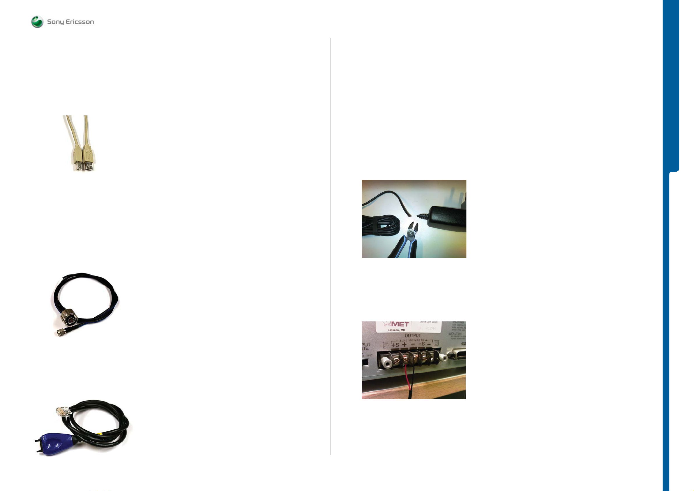
USB Computer Cable
Location: CSPN-Repair Instructions-Level: Mechanical-Tool Catalogue
See Picture 4.
Picture 4
DSU-60/USB Cable
Location: CSPN-Repair Instructions-Level: Mechanical-Tool Catalogue
Part number: KRY 101 1413
RF Test Cable Flexible
Location: CSPN-Repair Instructions-Level: Mechanical-Tool Catalogue
Part number: RPM 119 885
See Picture 5.
Power Cable RED to Power Supply Channel 1 VBATT
Maximum Length: 1m
Location: CSPN-Repair Instructions-Level: Mechanical-Tool Catalogue
Power Cable BLACK to Power Supply Channel 1 VBATT
Maximum Length: 1m
Location: CSPN-Repair Instructions-Level: Mechanical-Tool Catalogue
Customized Power Supply Channel 2 DCIO/SEPI Cable
To perform Current Calibration the phone must be supplied directly through the system
connector. Customize the cable according to following instructions:
STEP 1:
Take the CST-75 battery charger and cut off the charger according to Picture 7.
Picture 7
TROUBLESHOOTING
Picture 5
SEPI Interface Cable – A1
Location: CSPN-Repair Instructions-Level: Mechanical-Tool Catalogue
Part number: KRY 101 1119/1
See Picture 6.
Picture 6
Note: Cable length must be exact 1.3m.
STEP 2:
Connect the CST-75 charger Red or White wire to the Plus Output and the Black wire to the
Minus (GND) Output at Power Supply Channel 2 DCIO/SEPI according to Picture 8.
Picture 8
1215-3608 rev. 1
5 (96)
TROUBLESHOOTING Equipment List
SEMC Troubleshooting Manual
K630 - V640 - K660
STEP 3:
Cut off isolation material from inside of the charger plug according to Picture 9.
Picture 9
STEP 4:
Connect DCIO and SEPI Interface Cable – A1 cables according to Picture 10.
Picture 10
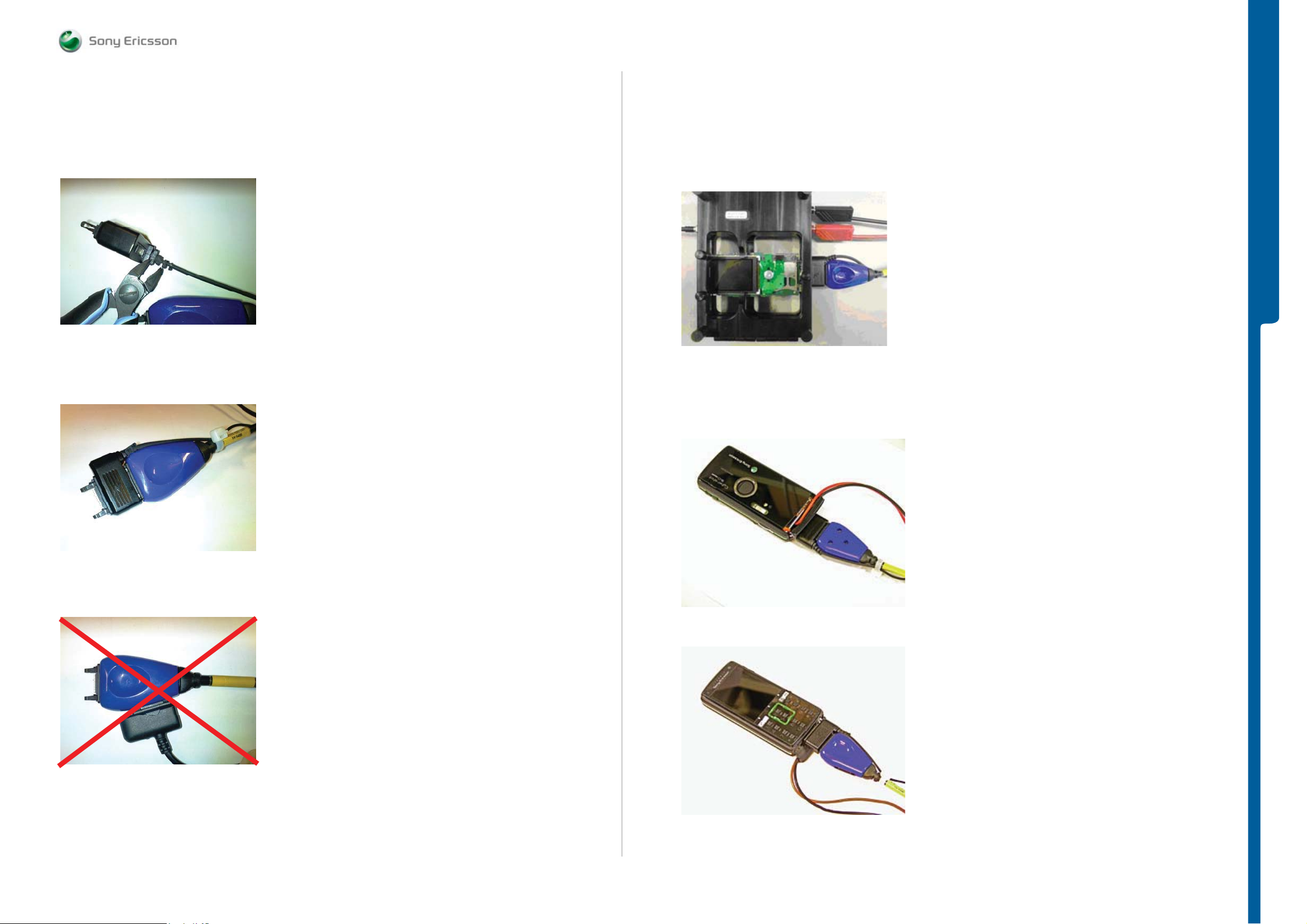
Power Supply Channel 2 DCIO/SEPI Cable Connection Setups
Correct DCIO/SEPI Cable setup when TRS Fixture is used.
Picture 12
TROUBLESHOOTING
Note: Example of DCIO/SEPI and K750 TRS Fixture Setup.
Correct DCIO/SEPI Cable setup when the Dummy Battery is used.
Picture 13
Wrong setup.
Picture 11
Picture 14
1215-3608 rev. 1
6 (96)
TROUBLESHOOTING
Equipment ListEquipEquipment Listment List
SEMC Troubleshooting Manual
K630 - V640 - K660
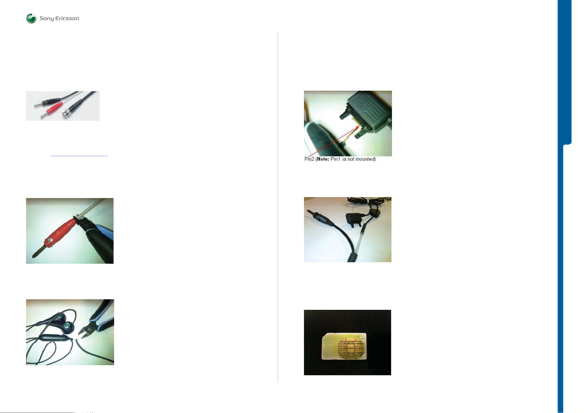
Customized FM Radio Cable
STEP 1:
Use Cable according to Picture 15
Picture 15
Product Name: Test lead BNC-4mm 1,5m
Product Description: Test lead with 4 mm lab plugs at one end and a BNC plug at the other.
Manufacturer: PMK Germany
Location: http://www.elfa.se/en/
or other supplier.
Part number: 46-310-40 (Note: This is ELFA part number)
STEP 2:
Cut the Red lab plug according to Picture 16
Picture 16
STEP 4:
Use only wire connected to Pin2 and cut all other wires according to Picture 18.
Use a digital multimeter instrument (DMM) and perform diode measurement to select the wire
connected to Pin2 at hands free system connector plug.
Picture 18
STEP 5:
Connect by soldering cable from Picture 16 and cable from Picture 18 according to Picture 19.
Picture 19
TROUBLESHOOTING
STEP 3:
Use any Portable Handsfree (PHF) Cable and cut according to Picture 17
Picture 17
Note: Minimum Cable length 40 cm.
Test Cards
Local SIM
Any functional Local SIM Card, see Picture 20
Picture 20
1215-3608 rev. 1
7 (96)
TROUBLESHOOTING Equipment List
SEMC Troubleshooting Manual
K630 - V640 - K660
Test SIM GSM/UMTS
One Test SIM GSM/UMTS is needed to perform Current Consumption Test, see Picture 21.
Location: To buy a Test SIM GSM/UMTS, please contact your supplier of test equipment.
Picture 21
Sony Memory Stick M2
Any functional Memory Stick Micro M2 Card, see Picture 22
Picture 22
SMK RF Probe
Location: CSPN-Repair Instructions-Level: Mechanical-Tool Catalogue
Part number: SXA 109 6356
Picture 24
TROUBLESHOOTING
Rohde & Schwarz RF Shield Package (Box)
Location: CSPN-Repair Instructions-Level: Mechanical-Tool Catalogue
Picture 23
1215-3608 rev. 1
8 (96)
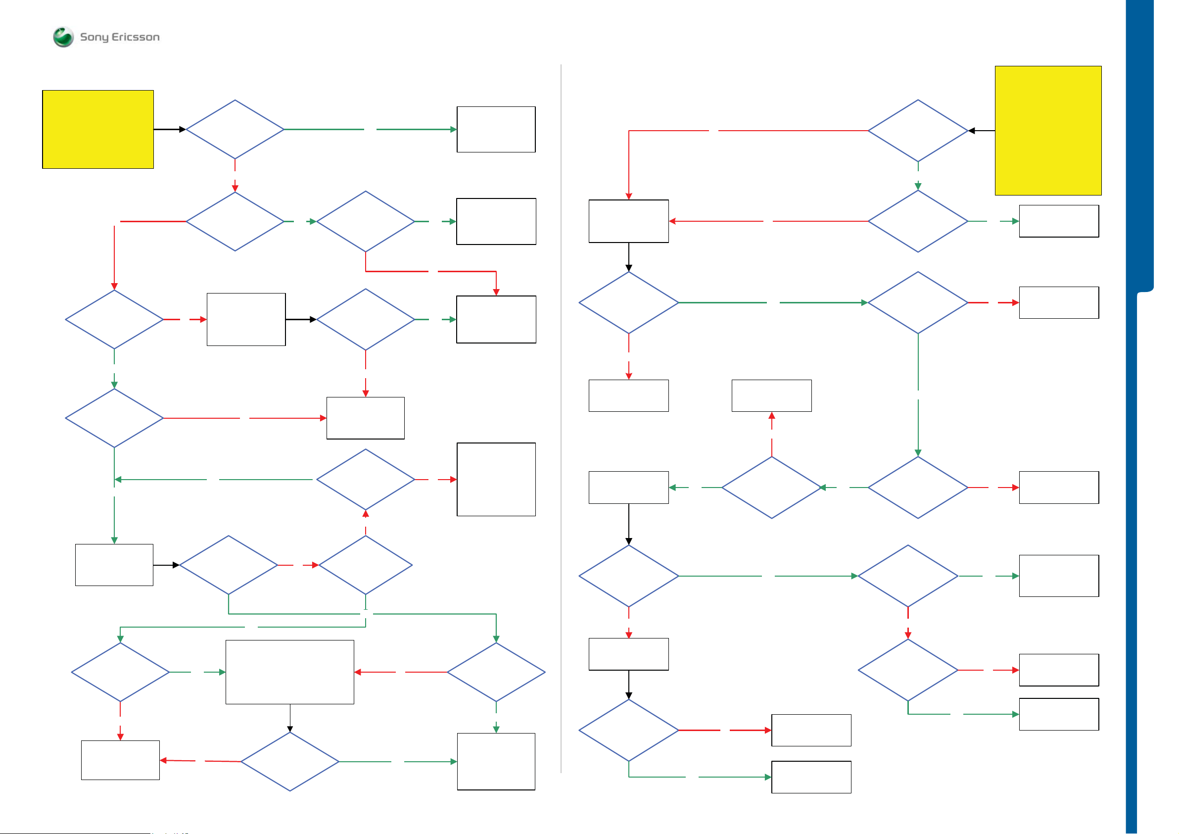
TROUBLESHOOTING On/Of f Prob lem s - Flash Proble ms
SEMC Troubleshooting Manual
K630 - V640 - K660
START
Connect:
Dummy Battery connected
to VBATT
No
Is the
phone consuming
any current when
powering on the
phone
On/Off problems
Is the phone
consuming more than
1mA when the phone
is powered off
No
Is it possible to
power on the phone
Connect a charger No
Yes
Yes
Is it possible to power
off the phone
Is the phones
behavior as normal
Optimized
charging
Yes
No
Yes
Go to
Dead phone
Problems part 1
Go to
Current
Consumption Test
After this go to
Charging Test.
Go to
Key problems
Power up the phone
Connect USB plug
From PC
The phone
Indicate charging
on display
No
No
Yes
Flash problems
Flash process
starting
when using
EMMA
Yes
Download
ITP SW
By using EMMA
Passed
3.8 Volt DC
at MP 107 (C2412)
VBATI
START
Step 1:
Perform System
Connector Protection Test
If successful go to step 2.
Try to Flash the phone by
Yes
No
Step 2:
Phone with Normal SW
Use TRS Fixture
Connect:
Display and Keypad
Connect: VBATT
using EMMA III SW
SL 5 Replace
D2020
SL 4 Escalate
SL 5 Replace
C2412
SL 4 Escalate
TROUBLESHOOTING
Yes
Is the current
consumption between
10mA to 70mA
Yes
Flash
the phone with
correct CDA
software
No
Yes
CDA Software
Flash
Successful
Yes
No
No
Go to
Dead Phone
Problems part 1
Press
2 and 5
Connect USB
Run Pre-config 1 and 2
Run DPY/Z
Successful
Flash
No
Flash process
started
Yes
No
Go to
System Connector
Protection Test..
After this go to
Flash problems
No
Go to USB/VBUS
Charging problems
Disconnect the
phone from
TRS Fixture
Max 35 Ohm between
MP 119 (X2400_Pin 10)
and MP 122 (R2432)
No
Yes
SL 5 Replace
D2404
SL 4 Escalate
No
3.5 Volt DC
at MP 103 (C2418)
VREG
Yes
Yes
Yes
1.8 Volt DC
at MP 105 (C2413)
VDDE18
Max 35 Ohm between
MP 120 (X2400_Pin 11)
and MP 123 (R2431)
No
No
Yes
SL 5 Replace
C2413
SL 4 Escalate
SL 5 Replace
D2404 if not Ok then
Replace D2000
SL 4 Escalate
Flash
The phone with
ITP software
successful
No
Go to
Flash problems
No
1. Customize the phone into DPY/Z
2. Startup the phone and wait for
the configuration to take place
(takes less than a minute)
3. Customize with correct CDA
4. Activate the phone
Problem
solved
NoYes
Yes
Problem
solved
Yes
Claim for a
SW Upgrade
Replace
System Connector
X2400
Problem
solved
Yes
No
SL 5 Replace
D2405
SL 4 Escalate
Claim
System Connector
X2400
Is the
R2431 and R2432
Ok
Yes
SL 5 Replace
No
R2431 or R2432
SL 4 Escalate
SL 5 Replace
SL 4 Escalate
1215-3608 rev. 1
D2405
9 (96)
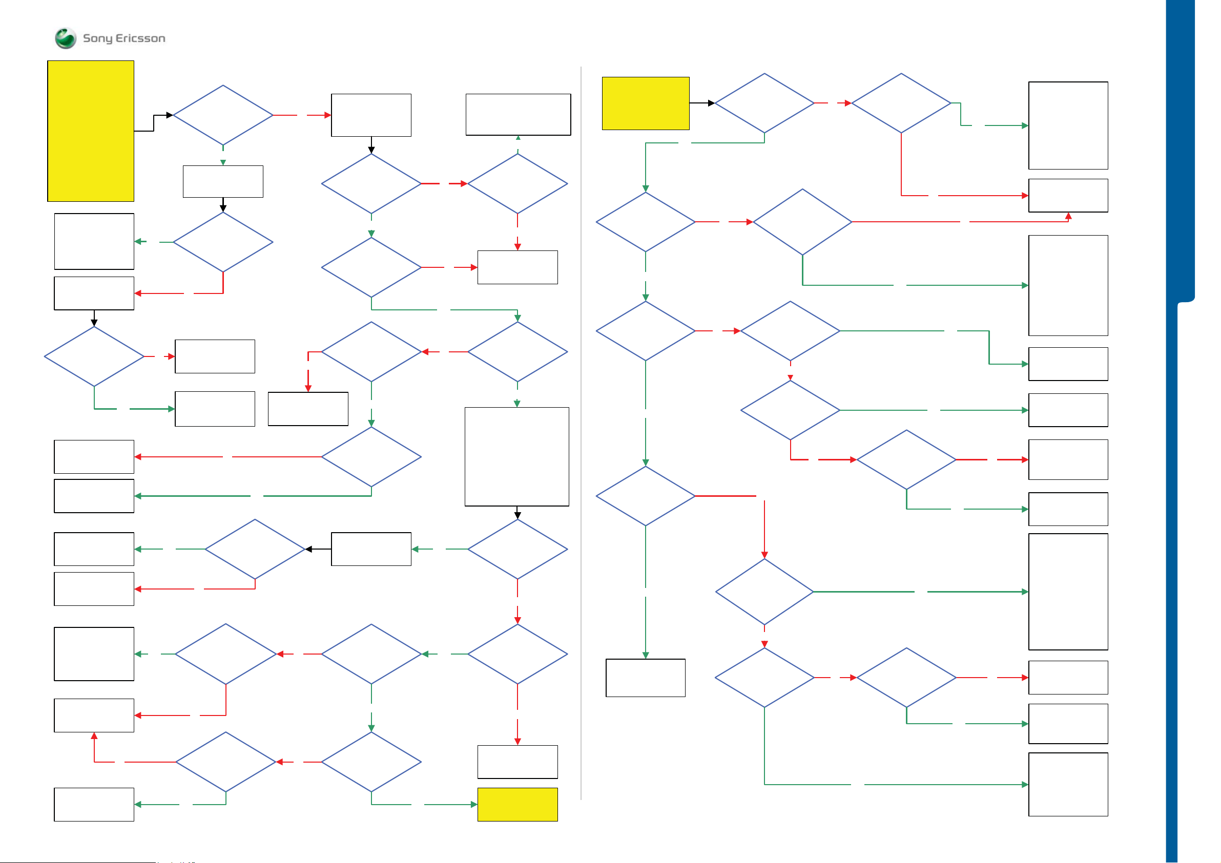
TROUBLESHOOTING
Dead Phone Problems
SEMC Troubleshooting Manual
K630 - V640 - K660
START
Step 1:
Try to recover the phone
using EMMA III SW
Press keys 2 and 5
Connect USB Cable
Run pre-config 1 or 2
Run DPY/Z
Step 2:
Use TRS Fixture
Connect VBATT
NOTE:
Do NOT use
DCIO/SEPI Cable!
K660: Replace
N1002 or N1210
K630/V640: Replace
N1210 or
SL 5 Replace N1002
SL 4 Escalate
SL 5 Remove
N2000
SL 4 Escalate
Using more than
1 mA
current
Yes
No
Dead Phone problems part 1
S2400
Not pressed
Using more than
1mA
current
Yes
Try to trace the
faulty component
with freezing spray
N1002 or N1210
getting hot
No
SL 5 Replace
N2000
SL 4 Escalate
No
No
Keep S2400
Pressed or
Connect
DCIO/SEPI Cable
32 kHz RTCCLK at
MP 43 (B2100_Pin7)
Yes
32 kHz RTCCLK at
MP 22 (ST2105)
0 Volt
Between Power
Supply GND and
PBA GND
No
Yes
No
No
K660: Replace B2 100
K630/V640:
SL 5 Replace B2100
SL 4 Escalate
Yes
2.2 Volt at
MP 14 (B2100_Pin1
VDD_LP)
No
SL 5 Replace
N2000
SL 4 Escalate
26 MHz
MCLK at
MP R2106
Dead Phone problems
Part 2
(Dead Phone Problems
Part 1 must be finished
before starting here)
VDIG
Voltage
Ok
Yes
VCORE18
Voltage
Ok
Yes
No
No
Dead Phone problems part 2
VBT27
Voltage
Ok
Are any of
C2215,C4213,
C1407, N1400
Short circuit
Are any of
C2342 to C2347
or D2000
Short circuit
No
No
Are any of
C2205,
N1400, C1409
Short circuit
Yes
No
Yes
No
Yes
K630/V640:
SL 5 Replace N1400
C2205 or C1409
SL 4 Escalate
K660:
SL 4 Replace N1400
SL 5 Replace
C2205 or C1409
SL 4 Escalate
SL 5 Replace
N2000
SL 4 Escalate
K630/V640:
SL 5 Replace
N1400, C2215,
C4213 or C1407
SL 4 Escalate
K660:
SL 4 Replace N1400
SL 5 Replace
C2215, C4213 or
C1407
SL 4 Escalate
SL 5 Replace
Faulty Component
SL 4 Escalate
TROUBLESHOOTING
Yes
SL 5 Replace
N2000
SL 4 Escalate
Replace
N1200
SL 5 Replace
D2020
SL 4 Escalate
Go to
Flash Problems
SL 4 Replace
N2400
SL 5 Replace
C2400, C2430,
C3135 or C3136
SL 5 Replace
N2000
SL 4 Escalate
No
SL 5 Replace
Faulty Component
SL 4 Escalate
Yes
Try to trace the
faulty component
with freezing spray
Yes
No
C2400, C2209,C2430,
C3135,C3136
Short circuit
No
C2326, C2327,
C2328, C2329, C2330,
C2216,D2000
Short circuit
Yes
No
Flash process
successful
N2400
Yes
SL 5 Replace
R2200
SL 4 Escalate
No
No
Yes
1.8V DC at
MP 33 (ST2208 VDDE18)
2.8V DC at
MP 36 (R2202
VccA)
Try to recover the
phone using
SW Load ITP
AUDIO26
Voltage
Ok
Yes
VANA25
Voltage
Ok
Yes
Yes
Check these voltages:
2.6V MP 41 (ST2204 AUDIO26)
2.5V MP 34 (ST2203 VANA25)
2.7V MP 37 (ST2212 VBT27
2.7V MP 38 (ST2213 VDIG)
1.8V MP 15 (ST2217 VCORE18)
1.2V MP 12 (ST2221 VCORE12)
All voltages
Yes
consumption more
SL 5 Replace
SL 4 Escalate
Dead Phone
problems part 2
Yes
Ok
No
Current
than 50mA
No
N2000
Go to
Yes
VCORE12
Voltage
Ok
Yes
Try to Recover the
Phone by
downloading
ITP SW
1.8 Volt DC at
MP 15 (ST2217)
No
MP 12 (ST2221)
Short circuit
To PBA GND
No
1.2 Volt DC at
MP 23 (V2206)
No
No
Yes
3.8 Volt DC at
MP 13 (ST2216)
Yes
3.8 Volt DC at
MP 24 (L2201)
Yes
Yes
Yes
No
No
SL 5 Replace
C2239
SL 4 Escalate
SL 5 Replace
C2238 and N2202
SL 4 Escalate
SL 5 Replace
N2202
SL 4 Escalate
SL 5 Check
C2301 to C2305,
C2307,C2308,
C2311
C2313 to C2319
C2322,C2324,D2000
SL 5 Replace
Faulty Component
and L2200
SL 4 Escalate
SL 5 Replace
L2201
SL 4 Escalate
SL 4 Replace
V2206
SL 5 Replace
N2000
K630/V640:
SL 5 Replace
L2200
SL 4 Escalate
K660:
Replace L2200
1215-3608 rev. 1
10 (96)
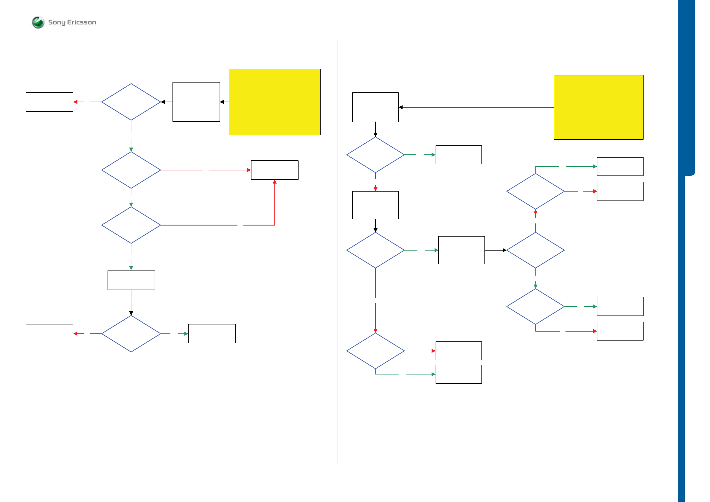
TROUBLESHOOTING Display Problems - Display Illumination Problems
SEMC Troubleshooting Manual
K630 - V640 - K660
Go to
Display illumination
problems
No
Display problems
Display Backlights
Ok
Yes
1.8 Volt DC
at
MP 8 (ST4200
VDDE18)
Yes
2.7 Volt DC
at
MP 6 (ST4201
VDIG)
Yes
Fault trace SW
MMI
Display pattern
Init Screen Testing
Activate:
RGB Color Pattern
No
START
Step 1:
Use TRS Fixture and connect Display and
Keypad. If Display working properly at the
fixture then replace Display
If not then continue with the
Step 2:
Load ITP SW into the phone
Use TRS Fixture and connect Display
Connect: VBATT and DCIO/SEPI
Continue with the
Display problems TRS guide
SL 5 Replace
N2000
SL 4 Escalate
No
Fault trace SW
MMI
Misc
Activate:
Display Backlight
Display Backlights
Ok
No
Fault trace SW
MMI
Misc
Deactivate:
Display Backlight
3.8 Volt DC at
MP 95 (TP4200)
Yes
Yes
Display Illumination problems
Flash the phone with
EMMA
SUCR SW
Fault trace SW
MMI
Misc
Activate:
Display Backlight
4.3V
Pk-Pk Pulses
(± 0.5V) at MP 21 (L4200)
short after Display
Backlight
Is set
No
15V Pk-Pk
Pulses at MP 95 (TP4200)
short after Display
Backlight
Is set
START
Use TRS Fixture and connect Display and
Keypad. If Display working properly at the
fixture then replace Display
Load ITP SW into the phone
Use TRS Fixture and connect Display
Connect: VBATT and DCIO/SEPI
Display illumination problems TRS guide
Yes
Step 1:
If not then continue with
Step 2:
Continue with the
SL 5 Replace
V4200
SL 4 Escalate
SL 5 Replace
No
N2000
SL 4 Escalate
TROUBLESHOOTING
SL 5 Replace
D2000
SL 4 Escalate
Replace
X4200
No Yes
Display
Ok
Claim Component
X4200
No
3.8 Volt DC at
MP 19 (V4201
Anode)
Yes
No
SL 5 Replace
L4201
SL 4 Escalate
Replace
V4201
Yes
0 Volt DC at
MP 94 (TP4201) when
Display Backlight Is
On
No
Yes
Replace
X4200 or Display
SL 5 Replace
V4206 or N2000
SL 4 Escalate
1215-3608 rev. 1
11 (96)
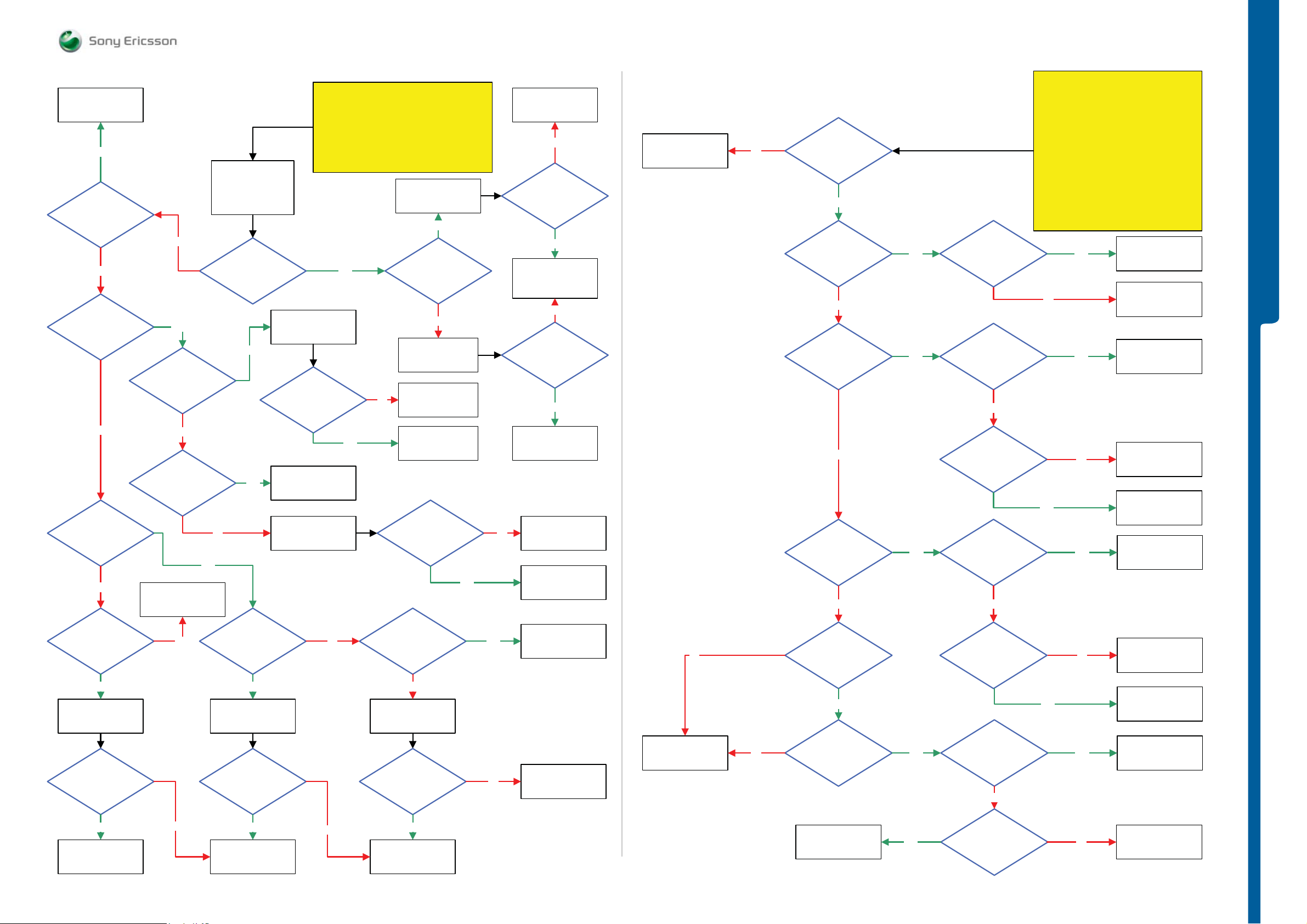
TROUBLESHOOTING Key Problems - LED Problems
SEMC Troubleshooting Manual
K630 - V640 - K660
SL 5 Replace
V2402
SL 4 Escalate
Yes
Problem with
Phone Off
No
Problem with
Volume Down
key
No
Problem with
Volume Up
key
No
Problem
With all other
keys
No
Yes
More than
2.0 Volt DC between
MP 83 (S2402 A) and
MP 82 (S2402
C)
No
Short
Circuit between
MP 83 (S2402 A)
MP 92 (PBA GND) and
MP 82 (S2402 C)
MP 92 (PBA
GND)
No
Yes
Flash the Phone with
EMMA
SUCR SW
No
2.0 Volt DC between
MP 80 (S2403 A) and
DMM Settings:
Diode
Measurement
Problem with
Phone On
Yes
MP 83 (S2402 A) and
Yes
More than
MP 79 (S2403
C)
Key problems
Use TRS Fixture and connect Display and
Perform Keyboard Test in Service Tests
If All Keys working properly at the
TRS Fixture then replace Keypad. If not then
disconnect VBATT and continue with the
Yes
Press the
Volume Down key
S2402
0 Volt
DC between
MP 82 (S2402
C)
Replace
V3107 or V3108
Remove
S2402
No
START
Step 1:
Keypad. Connect: VBATT
Key problems TRS guide
Press the On/Off
Key S2400
the black probe
To PBA GND
more than 1.7 Volt DC at
MP 46 (V2409
Cathode)
Remove
No
Yes
MP 92 (PBA GND) and
Circuit between
MP 80 (S2403 A)
MP 79 (S2403 C)
Replace
SL 5 Replace
SL 4 Escalate
More than
2.0 Volt DC between
MP 83 (S2402 A) and
MP 82 (S2402
Short
MP 92 (PBA
GND)
Yes
Connect
No
S2400
S2402
D2000
C)
Yes
0 Volt DC at MP 46
(V2409_Cathode)
1.7 Volt DC at MP 46
(V2409_Cathode)
No
Yes
Replace
S2400
No
Yes
SL 5 Replace
L2406, V2409
or N2000
SL 4 Escalate
No
More than
Yes
Replace
S2400
SL 5 Replace
D2000
SL 4 Escalate
Replace
S2402
Replace
V3109 or V3110
Go to
Display illumination
problems
No
Display
Backlight
Ok
Yes
Problem
with all
Keypad LED
No
Problem with
Lower Keypad LED
No
Problem with
Upper Keypad LED
No
K660 No
LED problems
Yes
Yes
Yes
0 Volt DC at
MP 78 (TP2003)
0 Volt DC at
MP 77 (TP2004)
No
0 Volt DC at
MP 18 (V4205_Pin 1)
0 Volt DC at
MP 78 (TP2003)
No
0 Volt DC at
MP 20 (V4205_Pin 4)
Load ITP SW into the phone.
START
Use TRS Fixture and connect
Keypad and Display
Connect: VBATT and DCIO/SEPI
Use Fault Trace SW
MMI
Activate:
Upper Keypad LED, Lower Keypad LED
If all Keypad LED working properly at the
No
Yes
Display Backlight
Web Navigator LED
TRS Fixture then replace Keypad
If not then continue with the
LED problems TRS guide.
Yes
Yes
No
Yes
No
Replace
X2402
SL 5 Replace
N2000
SL 4 Escalate
Replace
X2402
SL 5 Replace
N2000
SL 4 Escalate
SL 5 Replace
V4205
SL 4 Escalate
Replace
X2402
SL 5 Replace
N2000
SL 4 Escalate
TROUBLESHOOTING
Yes
Replace
X2402
Problem
solved
Yes
Claim Component
X2402
No
Yes
Press the
Volume Up key
S2403
0 Volt DC
between
MP 80 (S2403 A) and
MP 79 (S2403
C)
Yes
SL 5 Replace
D2000
SL 4 Escalate
No
No
Remove
S2403
More than
2.0 Volt DC between
MP 80 (S2403 A) and
MP 79 (S2403
C)
Yes
Replace
S2403
No
SL 5 Replace
D2000
SL 4 Escalate
Flash with
EMMA SUCR SW
No
Yes
Problem with
Web Navigator LED
SL 5 Replace
V4205
SL 4 Escalate
Yes
Yes
0 Volt DC at
MP 71 (TP2005)
No
0 Volt DC at
MP 16 (V4206_Pin 1)
Yes
Yes
No
1215-3608 rev. 1
SL 5 Replace
V4205
SL 4 Escalate
Replace
X2402
SL 5 Replace
N2000
SL 4 Escalate
12 (96)
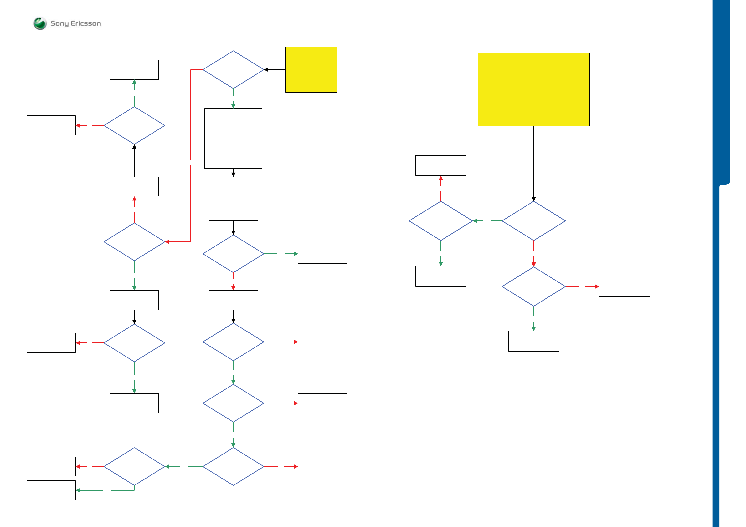
TROUBLESHOOTING Main and VGA Camera Problems - Vib r ator Proble ms
SEMC Troubleshooting Manual
K630 - V640 - K660
Replace
X4300
No
Main and VGA Camera problems
Claim
VGA Camera
Yes
VGA Camera
Ok
No
Replace
VGA Camera
No
Is the
problem with
Main Camera
Are there
problems with both
Main and VGA
Camera
Yes
Load ITP SW into the
phone. Use TRS Fixture
and connect Display.
Main and VGA Camera
mounted on the PBA.
Connect VBAT and
DCIO/SEPI
Use Fault Trace SW
Perform Main and VGA
Camera Test
Fault trace SW
MMI
Misc
Perform:
Main Camera Test
and
VGA Camera Test
Main and VGA
Camera working
properly
Service Tests and
Main and VGA
Camera Test
Yes
START
Go to
Perform:
Flash with EMMA
SUCR SW
Escalate
PBA
No
Connection
Between PBA
GND and MP 86
(ST4206)
Ok
Yes
Vibrator problems
START
Load ITP SW into the phone
Use TRS Fixture.
Connect: VBATT and DCIO/SEPI
Use Fault Trace SW and go to:
If the Vibrator is working properly at the
TRS Fixture then replace Vibrator if not
Continue with the Vibrator problems TRS guide
Yes
MMI-Misc
Activate:
Vibrator Test
2.8 Volt
Pk-Pk Pulses At
MP 49 (C4206
VIBR_OUT)
No
TROUBLESHOOTING
Replace
X4310
No
Yes
Replace
Main Camera
Main Camera
Ok
Yes
Claim
Main Camera
No
Activate:
Main Camera Test
again
1.8 Volt DC
at MP 47 (R2280
CAM_LDO_EN) and
MP 88 (TP4300
CAMRESn)
Yes
1.3 Volt DC
at MP 61 (TP2205
VCAMSD13)
Yes
No
No
SL 5 Replace
D2000
SL 4 Escalate
Replace
N2204
Clean Pad B4200 A
Clean Pad B4200 B
Is
MP 49 (C4206)
short circuit to
Ground
Yes
SL 5 Replace
C4206, C4207,V4203
SL 4 Escalate
No
SL 5 Replace
N2000
SL 4 Escalate
SL 5 Replace
D2000
SL 4 Escalate
Retest
Main and VGA
Camera
No
13MHz at
MP 11 (L4202)
19MHz at MP 84
(ST4312) and MP 1
(ST4314)
Yes
Yes
2.8V DC at MP 59
(TP2206 VCAMSD28)
1.8V DC at MP 58
(TP2207 VCAMSD18)
No
Replace
N2203
1215-3608 rev. 1
13 (96)
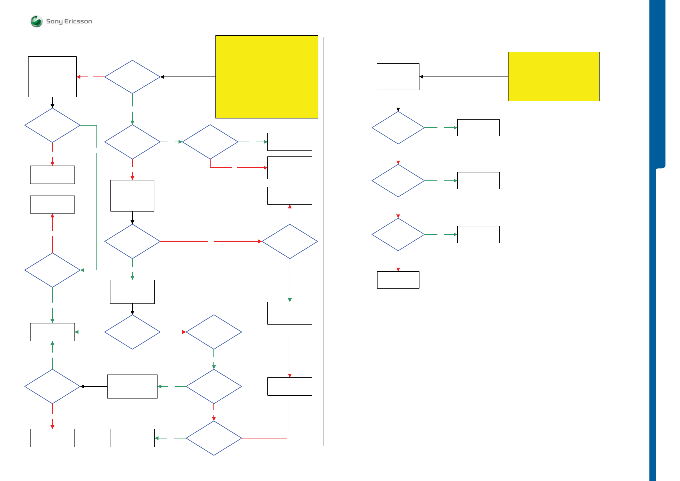
TROUBLESHOOTING Charging Problems - USB /VBUS Char gi ng Prob lem s
SEMC Troubleshooting Manual
K630 - V640 - K660
Use TRS Fixture and
Fault Trace SW
Connect:
VBATT and
DCIO/SEPI
Start
Battery Calibration
Is the
3.2V and 4.1V DC
at MP 89 (TP2200)
during Battery
Calibration
No
Replace
X2200
SL 5 Replace
R2200
SL 4 Escalate
No
Yes
Charging problems
Battery Calibration
Passed
Yes
Current Calibration
Passed
No
Use TRS Fixture
Fault Trace SW
Connect:
VBATT and
DCIO/SEPI
Yes
instrument settings instructions when performing
Is
MP 87 (TP2202)
Short circuit to
PBA GND
START
Perform System Connector Protection Test
If successful go to step 2.
Load ITP SW into the phone
Connect: Dummy Battery
Connect:VBATT and DCIO/SEPI
Battery and Current Calibration
It is very important to follow
the Battery and Current Calibration Test.
No
Step 1:
Step 2:
Use Fault Trace SW:
Logic, Phone Power
Perform
SL 5 Replace
Yes
SL 4 Escalate
Flash the phone with
EMMA SUCR SW
and go to
Charging Test
Replace
System Connector
N2000
X2400
No
Connect
DSU-60/USB Cable
from PC to
the phone
5 Volt DC at
MP 25 (ST2201)
No
D2405
Getting hot
No
USB/VBUS Charging problems
Yes
Yes
SL 5 Replace
N2000
SL 4 Escalate
SL 5 Replace
D2405
SL 4 Escalate
START
Step 1:
Perform System Connector Protection Test
If step 1 is Ok then continue with step 2.
Step 2:
Use Phone with Normal SW
Use TRS Fixture
Connect: VBATT
TROUBLESHOOTING
No
Is
Connection
between PBA GND
and Power Supply
VBATT GND
Ok
Yes
SL 5 Replace
N2000
SL 4 Escalate
Yes
Is
R2201
0.3 Ohm
Yes
5 Volt DC at
MP 126 (C2201)
DCIO
Yes
Start
Current Calibration
(C.C.)
The Phone
Consuming
DCIO Current
(During Current
Calibration)
Disconnect
VBATT and DCIO/SEPI
consuming more
No
MP 28 (C2241
No No
Yes
DCIO_INT)
Higher than
3,8 Volt DC
Yes
MP 126 (R2201
CHSENSEP) Higher
than 3,8 Volt DC
(During C.C.)
than 10mA
Charger (DCIO)
Current
SL 5 Replace
C2423 and C2424
SL 4 Replace
SL 5 Replace
SL 4 Escalate
Phone
Yes
V2421
N2000
5 Volt DC at
MP 76 (R2409)
No
Replace
System Connector
X2400
Yes
SL 5 Replace
R2409
SL 4 Escalate
No
SL 5 Replace
R2201
SL 4 Escalate
Replace
V2202
No
MP 109
(V2202_Pin 2
Yes No
CHREG) Lower than
MP 28 (C2241)
(During C.C.)
1215-3608 rev. 1
14 (96)
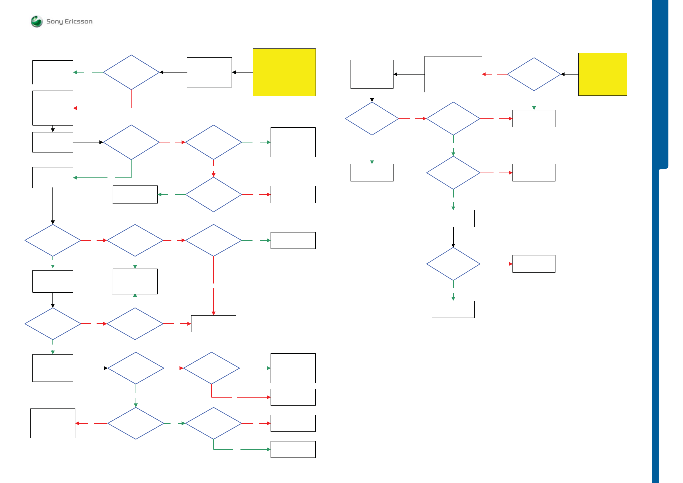
SIM problems
TROUBLESHOOTING
SIM Problems - Memory Stick Problems
Memory Stick problems
SEMC Troubleshooting Manual
K630 - V640 - K660
Flash the Phone
with EMMA
SUCR SW
Remove Test SIM
Disconnect:
Dummy Battery
Use TRS Fixture
and
Fault Trace SW
Activate:
SIMVCC
SIMVCC on
Activate:
SIMRST
Yes
Sim Com Test
Passed
No
1.8 Volt DC at
MP 98 (X2403_Pin 1)
Yes
SL 5 Replace
C2406 or C2411
SL 4 Escalate
Fault Trace SW
Logic
SIM Card control
Activate:
SIM Com Test
No Yes
Yes
1.8 Volt DC at
MP 99 (C2411)
No
Are any of
C2406 or C2411
Short circuit
Load ITP SW into the phone.
No
Connect:
Dummy Battery to VBATT
Insert Test SIM
Connect:
DCIO/SEPI
Use Fault Trace SW
K630/V640:
SL 5 Replace X2403
SL 4 Escalate
K660:
Replace X2403
SL 5 Replace
N2000
SL 4 Escalate
START
Fault trace SW
Logic
SIM Card Control
Activate:
Memory Stick Test
Memory Stick Test
Passed
Yes
Flash the phone with
EMMA
SUCR SW
Load ITP SW into the phone
Use TRS Fixture
VBATT and DCIO/SEPI
Insert Memory card
Use Fault Trace SW
No
MP 32 (R2406
MSDETECT)
at MP 35 (ST2202)
VMC18 only 30 sec
after card has been
Connect :
0 Volt DC at
Yes
1.8 Volt DC
inserted
Yes
Replace
X2490
No
No
No
Is
X2490
damaged
Yes
Replace
X2490
SL 5 Replace
N2000
SL 4 Escalate
START
TROUBLESHOOTING
1.8 Volt DC at
MP 100 (X2403_Pin 2)
Yes
SIMVCC on
SIMRST on
Activate:
SIMCLK
1.0 Volt DC at
MP 102 (X2403_Pin 3)
Yes
SIMVCC on
SIMRST on
SIMCLK on
Activate:
SIM DATA
No
No
1.8 Volt DC at
MP 104 (C2410)
Yes
K630/V640:
SL 5 Replace X2403
SL 4 Escalate
K660:
Replace X2403
Yes
1.0 Volt DC at
MP 30 (ST2400)
1.8 Volt DC at
MP 97 (X2403_Pin 7)
Yes
No
No
No
Is
C2410
Short circuit
No
SL 5 Replace
N2000
SL 4 Escalate
1.8 Volt DC at
MP 29 (ST2401)
No
Yes
Yes
SL 5 Replace
C2410
SL 4 Escalate
K630/V640:
SL 5 Replace X2403
SL 4 Escalate
K660:
Replace X2403
SL 5 Replace
N2000
SL 4 Escalate
Problem solved
Yes
Claim Component
X2490
No
SL 5 Replace
D2000
SL 4 Escalate
K630/V640:
SL 5 Replace X2403
SL 4 Escalate
K660:
Replace X2403
No
MP 96
(X2403_Pin 5)
Connected to the
PBA GND
Yes
10 Kohm between
MP 98 (X2403_Pin1)
(Red Probe) and MP 97
(X2403_Pin 7)
(Black Probe)
Yes
No
SL 5 Replace
R2419
SL 4 Escalate
SL 5 Replace
N2000
SL 4 Escalate
1215-3608 rev. 1
15 (96)
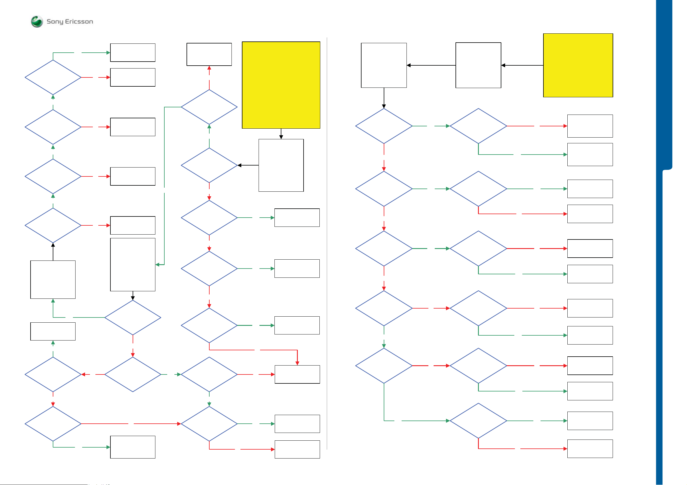
TROUBLESHOOTING Audio Internal Problems - Audio External Proble ms
SEMC Troubleshooting Manual
K630 - V640 - K660
2.6 Volt DC
At MP 121 (V2420)
Yes
2.6 Volt DC
At MP 17
(V2405_Pin 3)
Yes
0 Volt DC
At MP 17
(V2405_ Pin 3)
Yes
0 Volt DC
on both side
of MP 7 (R2456)
Fault Trace SW
Logic
GPIO Manager
Access:
Set GPIO_07 to Low
Application:
Set GPIO_01 to Low
Yes
SL 5 Replace
L3108 and L3109
SL 4 Escalate
Yes
1.9 Volt DC
At MP 48 (TP3104)
and MP 53 (TP3105)
No
Audio Internal problems
Go to
Yes
No
No
No
No
No Yes
Audio External
Problems
SL 5 Replace
R2440
SL 4 Escalate
Replace
V2405
Replace
N2400
SL 5 Replace
D2000
SL 4 Escalate
Fault Trace SW
Audio and FM Radio
Audio Loop test
Audio Input: Mic1
Loop Mode: Analog
Audio Output:
Loudspeaker
Apply Audio Loop
Whistle into the
PBA Mic
More than
100mVolt AC Pk-Pk
At MP 50 (X3102) and
MP 51 (X3103)
No
1.9 Volt DC
At MP 50 (X3102)
and MP 51
(X3103)
Yes
SL 4 Replace
V3101 or V3102
SL 5 Replace
L3103 or L3104
No
More than
100m Volt AC Pk-Pk
at MP 3 (X3100) and
MP 2 (X3101)
Yes
More than
100m Volt AC Pk-Pk at
MP 4 (L3103 BEARP)
and MP 5 (L3104
BEARN)
No
More than
100mVolt AC Pk-Pk at
MP 108 (TP3101)
No
2.2 Volt DC
At MP 39 (R3131)
No
Are any of
V3103 and V3104
Short circuit
More than
100mVolt AC Pk-Pk
At MP 44 (C3137) and
MP 45 (C3123)
Yes
START
System Connector Protection Test
Use TRS Fixture connect Display and
Keypad. Connect VBATT and perform
Service Tests working properly at the
fixture then replace Loudspeaker or
and continue with the Audio internal
Step 1: Perform
Step 2:
Audio Service Tests. If all Audio
Earphone
Load ITP SW into the phone.
Connect VBATT and DCIO/SEPI
Yes
Yes
Yes
No
If not then
Use TRS Fixture.
problems TRS guide
Fault Trace SW
Audio and FM Radio
Audio Loop test
Audio Input: Mic1
Loop Mode: Analog
Audio Output:
Earphone
Apply Audio Loop
Whistle into the
PBA Mic
SL 5 Replace
N2000
SL 4 Escalate
Replace
B3100
Replace
V3103 or V3104
No
SL 5 Replace
N2000
SL 4 Escalate
Disconnect
DCIO/SEPI cabel
Insert PHF set
Talk into the AUX
mic
Can you
hear at AUX
earphone when you
speak into the
AUX mic
No
More than
100mV AC Pk-Pk
At MP 117 (L2403 SPL)
and MP 118 (L2404 SPR)
When whistle in to the
AUX mic
No
More than
100mV AC Pk-Pk at MP
124 (C3124 MICP_int)
and MP 110 (C3125
MICN_int)
No
Is MP 115
(X2400_Pin 3
connected to MP 113
(L2401)
Yes
Is MP 116
(X2400_Pin 4)
connected to MP 114
(L2402)
Audio External problems
Fault trace SW
Audio and FM Radio
Audio Loop Test
Audio Input: AUX1
Loop Mode: Analog
Audio Output:
AUX Earphone
Apply Audio Loop
Yes
Yes
Yes
No
No No
Audio Internal
Tested
Are any of
L2403 or L2404
damaged
More than
100mV AC Pk-Pk At
MP 125 (C3113) and
MP 101 (C3120)
L2401
Ok
L2402
Ok
No
Yes
Yes
No
No
Yes
No
Yes
Yes
START
Step 1: Perform
System Connector Protection
Test
Step 2:
Load ITP SW into
the phone.
Use TRS Fixture
Connect: VBATT and DCIO/SEPI
Use Fault Trace SW
TROUBLESHOOTING
Go to
Audio Internal
problems
Flash the phone
with EMMA
SUCR SW
Replace
L2403 or L2404
Replace
System Connector
X2400
SL 5 Replace
N2000
SL 4 Escalate
Replace
N3101
Replace
L2401
Replace
System Connector
X2400
Replace
L2402
Replace
System Connector
X2400
Are any of
V3105, V3106
C3137 and C3123
short circuit
Yes
No
SL 4 Replace
V3105 or V3106
SL 5 Replace
C3137 or C3123
1.8 Volt DC
At MP 27 (R3137
AMPCTRL)
No
Yes
Replace
N3100
SL 5 Replace
D2000
SL 4 Escalate
Yes
2.2 Volt DC at
MP 75 (C3169)
No
Yes
Replace
N3101
SL 5 Replace
N2000
SL 4 Escalate
1215-3608 rev. 1
16 (96)
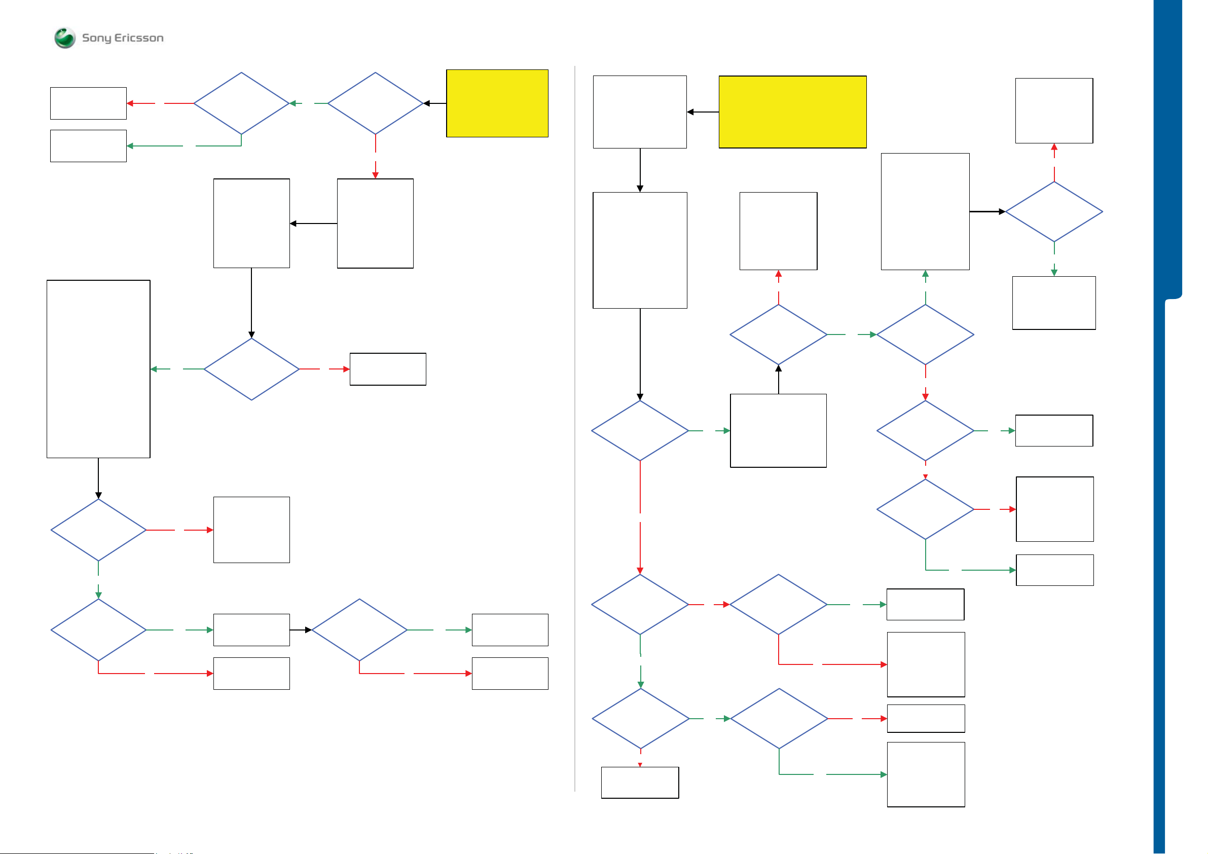
TROUBLESHOOTING FM Radio Problems - Bluetooth Problems
SEMC Troubleshooting Manual
K630 - V640 - K660
Replace
N3101
SL 5 Replace
N2000
SL 4 Escalate
Disconnect:
DCIO/SEPI Cable
Connect:
Customized FM Radio Cable
Black Lab Plug to
TRS Fixture GND Input and
PHF Connector to the Phone
System Connector
Signal Generator
Instrument Settings:
Frequency:
Use free Freq. Channel
Example:
103 MHz in Sweden
Amplitude: 25.0 uVrms
FM Dev: +/-22.5 kHz
FM Rate: 1kHz
Any signal at
MP 42 (C3145)
MP 40 (C3146)
Yes
Can you
hear 1KHz tone at
TRS Fixture
Loudspeaker
FM Radio problems
PHF
No Yes
Yes
No
Yes
No
working properly
during
Voice call
Yes
Fault trace SW
Audio and FM Radio
FM Radio
Audio Output
Loudspeaker
Frequency:
According to
Instrument Settings
Set FM Radio
3.8 Volt DC
at MP 68 (C3304)
and 1.8V at MP 65
(C3305)
SL 4 Replace
C3145 or C3146
SL 5 Replace
N1400
L3300 and C3303
SL 4 Escalate
Replace
System Connector
X2400
SL 5 Replace
N2000
SL 4 Escalate
Speaker and
FM Radio Tests
working properly
Load ITP SW
into the phone.
Use TRS Fixture
Connect VBATT and
DCIO/SEPI
Use Fault Trace SW
No
Signal Ok
No
SL 5 Replace
N2000
SL 4 Escalate
No
START
Go to
Service Tests and
Speaker and FM Radio Test
Yes
Perform:
Claim
System Connector
X2400
SL 5 Replace
R2405,L3301,L2400
SL 4 Escalate
Load ITP SW
Into the phone
Use TRS Fixture
Connect:
VBATT and DCIO/SEPI
Use Fault Trace SW
Fault trace SW
TX and RX
Bluetooth
Channel 0
Set MaxPwr MOD 0
Use
Spectrum Analyzer
Instrument settings:
Frequency: 2402 MHz
Span: 1MHz
Amplitude: -5dBm
Use Peak Search
Any Signal
at MP 112
(X2400_Pin 14)
BT_ANT
No
26 MHz Signal
At MP 10 (R2118
BT_CLK)
Yes
2.7 Volt DC at
MP 37 (ST2212
VBT27)
No
SL 5 Replace
N2000
SL 4 Escalate
Bluetooth problems
START
Flash the phone with the
EMMA SUCR SW and retest the phone.
If successful claim SW Flashing
If not then continue with
Bluetooth problems TRS guide.
K630/V640:
SL 5 Replace
N1400
SL 4 Escalate
K660:
Replace
N1400
No
Is
MOD 1 Freq.
minimum 230 KHz
higher then
MOD 0 Freq.
Fault Trace SW
TX and RX
Bluetooth
Yes
No
Yes No
Channel 0
Set MaxPwr MOD 1
Use Spectrum Analyzer
with the previous
instrument settings
More than
60KOhm between
MP 10 (R2118) and
PBA GND
1.8 Volt DC
At MP 33 (ST2208
VDDE18) and 2.7 Volt DC
at MP 38 (ST2213
VDIG)
No
Yes
Yes
Yes
Change the
Bluetooth channels
In Fault Trace SW
and test the output.
Use
Spectrum Analyzer
Span 10MHz
Use Peak Search when
changing the channel.
Note:
1MHz channel spacing
Yes
-20dBm at
MP 112 (X2400_Pin 14
BT_ANT)
(±5dBm)
No
-10dBm at
MP 74 (Z1400_Pin 1)
(±5dBm)
No
-10dBm at
MP 72 (Z1400_Pin 5) and
MP 70 (Z1400_Pin 7)
(±5dBm)
Yes
SL 5 Replace
D2105
SL 4 Escalate
K630/V640:
SL 5 Replace
N1400
SL 4 Escalate
K660:
Replace
N1400
SL 5 Replace
N2000
SL 4 Escalate
K630/V640:
SL 5 Replace
N1400
SL 4 Escalate
K660:
Replace
N1400
System Connector
X2400 Pins 13 and 14
Yes
No
C1401 and L1403
K630/V640:
SL 5 Replace
N1400
SL 4 Escalate
K660:
Replace
N1400
No
TROUBLESHOOTING
All channels
passed
Yes
Replace
X2400
and clean
at PBA
SL 5 Replace
SL 4 Escalate
K630/V640:
SL 5 Replace
N1400
SL 4 Escalate
K660:
Replace
N1400
SL 5 Replace
Z1400
SL 4 Escalate
1215-3608 rev. 1
17 (96)
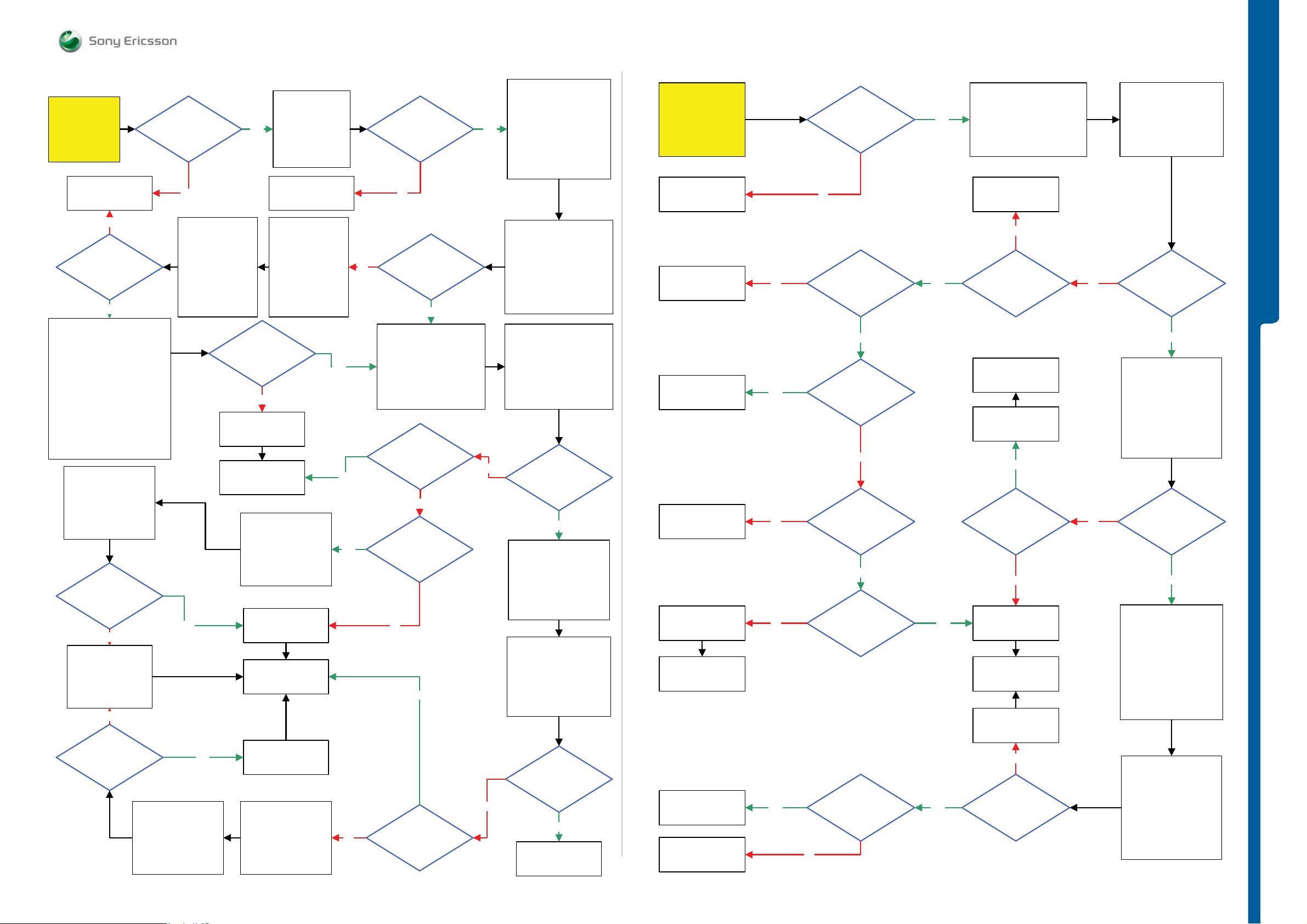
TROUBLESHOOTING GSM Network Proble ms - WCD MA Network Problem s
SEMC Troubleshooting Manual
K630 - V640 - K660
0 Ohm between
START
Replace
X1200
No
Is
Max Pwr 23dBm
Ok
(±3dBm)
Yes
Perform RSSI Test at
GSM 900, 1800 and 1900 Band
Instrument Settings
System Mode:
TX/RX Tester Mode (GSM)
GSM BAND:
E-GSM 900, Channel 124
E-GSM 900, Channel 975
DCS 1800, Channel 512
PCS 1900, Channel 512
RF Power ON: -60 dBm
Correction: -1.6 dBm
Measurement Mode:
Repeat,CW
Spectrum Analyzer
Instrument settings
Measure with RF
Probe
TX Freq. 824.2MHz
Span: 300KHz,
Amplitude: -5dBm
Signal at
MP 91 (Z1001)
-10dBm
5dBm)
(±
No
K630/V640:
SL 5 Replace N1002
SL 4 Escalate
K660:
Replace N1002
(Inside Thor)
No
Signal at
MP 90 (L1006)
-12dBm
(±5dBm)
MP 85 (R1208) and
Spectrum Analyzer
Instrument settings
Measure with RF
TX Freq. 1710.2MHz
Span: 300KHZ,
Amplitude: -5dBm
MP 81 (R1202)
Instrument
Settings:
System Mode:
TX/RX Tester Mode
(WCDMA)
Downlink Channel:
10562
Measurement
Mode: Repeat
Correction: 1.6 dB
Yes
Yes
Probe
GSM Network problems
Load the ITP SW
into the phone.
Yes
Fault Trace SW
Fault Trace SW
TX and RX WCDMA
Radio Settings:
Select Band:
Max Pwr 23dBm
All Bands
Passed
RSSI Test
No
Replace
N1200 Thor
Go to
SERP Calibration
Fault Trace SW
Switch GSM Mode
Settings to:
TX Static
Replace
N1200 Thor
Go to
SERP Calibration
Replace
N1200 Thor
Fault Trace SW
Switch GSM Mode
Settings to:
TX Static
Use fixture
Connect 3.8V
Limiter 2A
Use
SL 5 Replace
N2000
SL 4 Escalate
BAND I
Fast Select
Channels:
Ch LOW
Modes:
Yes
Yes
Yes
No
2.8 Volt DC
at MP 36 (R2202
VccA)
NoNo
No
RSSI Test
Passed
Yes
Instrument Settings:
System Mode:
TX/RX Tester Mode (GSM)
GSM BAND: GSM850
Measurement Mode:
Repeat, Burst
Correction: 1.6 dB
Is
measured value
±
5dBm
No
1.4V-1.6V
Pk-Pk pulses at
MP 93 (R1000
VAPC)
No
Yes
Is
measured value
5dBm
±
Connect Mobile Phone
Tester
Instrument Settings:
System Mode:
TX/RX Tester Mode (GSM)
Yes
No
No
GSM BAND: GSM850
RF Power ON: -60 dBm
Correction: -1.6 dBm
Measurement Mode:
Repeat, CW
Fault Trace SW
TX and RX GSM
GSM Mode Settings:
RX Switched
GSM Radio Settings:
Select Band :GSM 850
Channel: 128
GSM RSSI Measurements:
Start RSSI Test
Fault Trace SW
TX and RX GSM
GSM Mode Settings:
TX Switched
GSM Radio Settings:
Select Band : GSM 850
Channel : 128
Power Level: 5
measured value
33dBm
(±3dBm)
Instrument Settings:
System Mode:
TX/RX Tester Mode
(GSM)
GSM BAND: DCS1800
Measurement Mode:
Repeat, Burst
Correction: 1.6 dB
Fault Trace SW
TX and RX GSM
GSM Mode Settings:
TX Switched
GSM Radio Settings:
Select Band : GSM 1800
Channel : 512
Power Level: 0
measured value
30dBm
(±3dBm)
WCDMA Network
problems
Is
Yes
Is the
Yes
Go to
START
Replace
X1200
SL 5 Replace
D2000
SL 4 Escalate
Replace
N2205
SL 5 Replace
N2000
SL 4 Escalate
Replace
N1200
Go to
SERP Calibration
Replace
Faulty Component
Go to
GO-NOGO
Test
WCDMA Network problems
0 Ohm
between
MP 85 (R1208) and
MP 81 (R1202)
No
1.8Volt
DC at MP 55
No
Yes
No
No Yes
Yes
(R2299 DCDC_EN)
And 1.8V at MP 60 (C417
WPA0_EN)
(squid)
Yes
1.2V-1.8V DC at
MP 54 (R2221
WPAVCC)
No
2.7V-2.8V at
MP 36 (R2202 VccA)
1.8V at MP 33 (ST2208
VDDE18)
Yes
26MHz at
MP 62 (C511 WBCLK)
(inside Squid)
Are any of
X1201,X1202, X1203
X1001,X1002,X1003
damaged
No
Yes
Yes
Yes
Load ITP SW
into the phone.
Use TRS Fixture
Connect:
VBATT: 3.8V, Limiter 3A
DCIO/SEPI: 5V, Limiter 2A
Use Fault Trace SW
SL 5 Replace
R2210
SL 4 Escalate
No
3.4V-3.8V DC at
MP 57 (R2210
VBATI)
Go to
SERP Calibration
Replace
N1200
Yes
Current
consumption
between
450 – 650 mA
No
Replace
N1210
Go to
SERP Calibration
Replace
N1210
No
Phone report
correct value
(±5dBm)
No
No
Fault Trace SW
TX and RX WCDMA
Radio Settings:
Select Band: BAND I
Fast Select Channels:
Ch LOW
Modes: Max Pwr 23dBm
TROUBLESHOOTING
3.1V-3.3V DC at
MP 56 (L2207
VCC_WPA)
Yes
Instrument Settings:
System Mode:
TX/RX Tester Mode
WCDMA
Downlink Channel:
BAND I: 10562
Measurement Mode:
Repeat
Correction: 1.6 dB
Max Pwr.
23dBm
Ok
(±3dBm)
Yes
Instrument Settings:
System Mode:
TX/RX Tester Mode
WCDMA
Downlink Channel:
BAND I: 10700
Measurement Mode:
Repeat
RF Power ON: -60 dBm
Correction: - 1.6 dBm
Fault Trace SW
TX and RX WCDMA
Radio Settings:
Select Band : Band I
Fast select channels:
Ch MID
Modes: Read RSSI
RX On:
Read Measurement
1215-3608 rev. 1
18 (96)
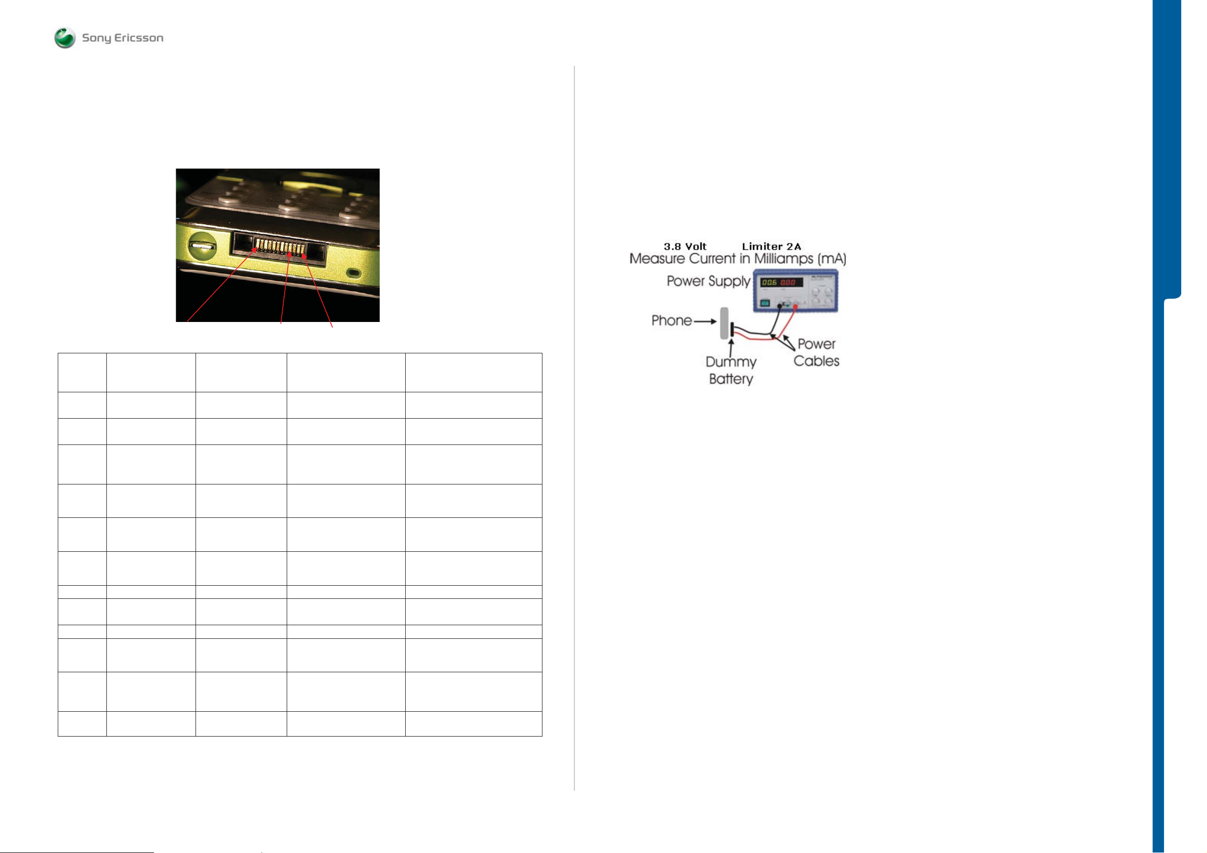
TROUBLESHOOTING System Connector Protect io n Test - Current Cons u mpt io n Test
SEMC Troubleshooting Manual
K630 - V640 - K660
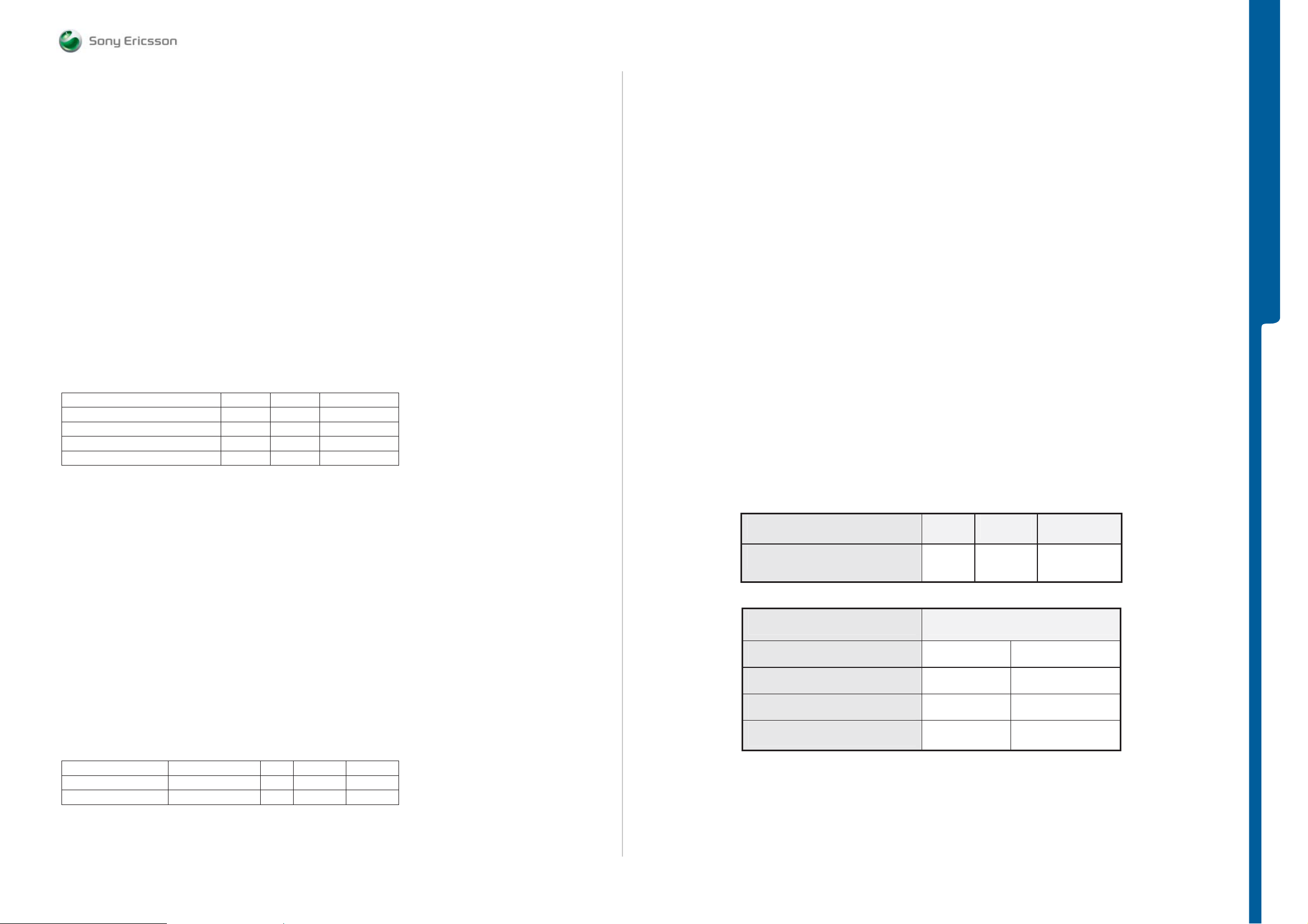
System Connector Protection Test
Perform Diode and Ohm measurements with a Multimeter
Connect the black probe at ground (Pin 9 on the system connector, X2400)
Pin 1
Diode
Pin at
X2400
1 0L 27K No Action
2 0.0 1.4 No Action
3 2.0 12K
4 1.0 1K
5 0.0 82
6 0.0 82
7 0L 0L Not connected Not connected
8 1.4 1.5K
9 0 0 No Action No Action
10 0L 430K No Action
Measurements
/ Volt
Measurements
/ Ohm
11 0L 470K No Action
12 0L 80K
Pin 9GND Pin 12
Ohm
SL 4 Action SL 5 Action
D2405 if lower than 27KΩ
R2433 if higher than 27KΩ
L2400 and L3301
If higher than 1.4Ω
N3101 if lower than
12KΩ L2401 if higher
than 12KΩ
N3101 if lower than
1KΩ L2402 if higher
than 1KΩ
N3101 if lower than
82Ω L2403 if higher
than 82Ω
N3101 if lower than
82Ω L2404 if higher
than 82Ω
V2420 if lower than
1.5KΩ
L2407 If higher than 12KΩ
L2408 if higher than 1KΩ
L2410 if higher than 82Ω
L2409 if higher than 82Ω
L2405, R2440, R2436
if higher than 1.5KΩ
D2405 if lower than 430KΩ
R2432 if higher than
D2405 if lower than
470KΩ R2431 if higher
than 470KΩ
V2421 if lower than
80KΩ
430KΩ
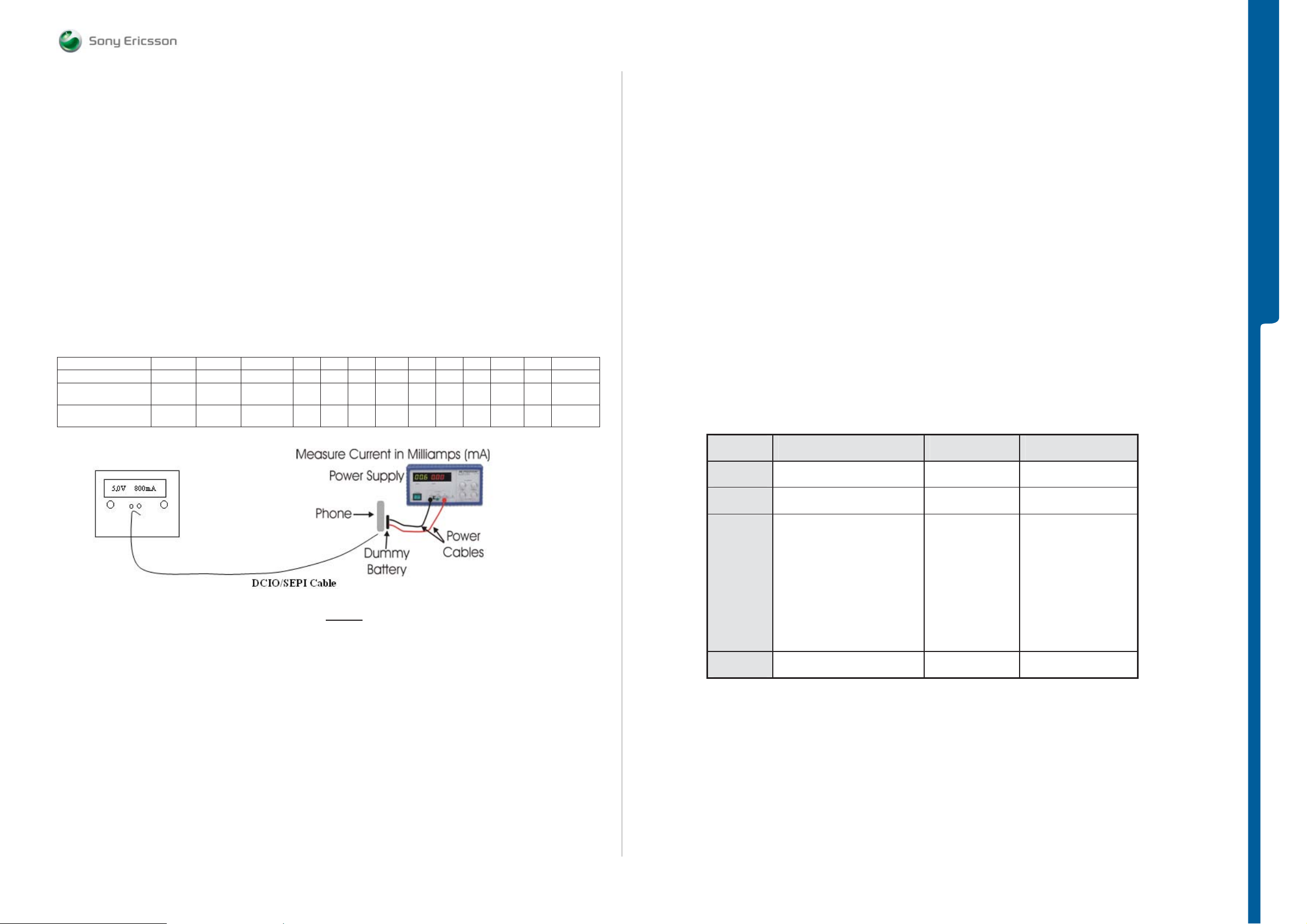
Current Consumption Test
Step 1:
Insert Local SIM Card and use the phone with the Normal SW (SSW) and dummy battery connected to
Power Supply Channel 1 VBATT according to Picture 1.
Instrument settings: Voltage: 3.8 Volt, Limiter 3A.
Measure the current when the Phone is off. Check the current consumption at Power Supply Channel 1
VBATT.
Picture 1
Current consumption in off mode should be less than 1mA.
If more than 1mA go to Dead Phone problems part 1 TRS guide.
Step 2:
Start the phone:
Measure the deep sleep current max 6mA typical between 0-3mA.
Make sure that the operator is running with deep sleep. (This operation can be switched off by operator if
the network is busy).
If the phone is using more than 6mA, then go to EMMA III and perform Software Update Contents Refresh
(SUCR).
Step 3 with Mobile Phone Tester Instrument
Insert Test SIM Card and use the phone with the Normal SW (SSW) and dummy battery connected to Power
Supply Channel 1 VBATT according to Picture 1.
Instrument settings: Voltage: 3.8 Volt, Limiter 3A.
Use the Mobile Phone Tester Instrument in signalling mode directly connected to the phone with the RF
Connector or use Shield Box if not possible. Phone Display must be on during these tests to get correct
current measurements.
Perform Radio TX measurements at GSM and WCDMA Band and compare the result with limits according to
the text below.
Transmitter current 850 MHz at Ch: 128 power level 5. Typical 400mA
Transmitter current 900 MHz at Ch: 1 power level 5. Typical 385mA
Transmitter current 1800 MHz at Ch: 512 power level 0. Typical 365mA
Transmitter current 1900 MHz at Ch: 512 power level 0. Typical 365mA
Transmitter current WCDMA BAND I Low RX Ch: 10562 at 23dBm output power Max 850mA
TROUBLESHOOTING
If the current consumption is not correct, the fault could be fixed by running SERP calibration if not then go
to GSM and WCDMA Network problems TRS guides.
If the current consumptions are equal to test limits then go to Charging Test.
1215-3608 rev. 1
19 (96)

TROUBLESHOOTING Current Consum pt io n Test
SEMC Troubleshooting Manual
K630 - V640 - K660
Step 4 with Fault Trace SW application:
-
Flash the phone with ITP SW
-
Use the TRS Fixture
-
Connect the:
Power Supply Channel 1 VBATT:
Instrument settings: Voltage: 3.8 Volt, Limiter 3A
Power Supply Channel 2 DCIO/SEPI
Instrument settings: Voltage: 5 Volt, Limiter 2A
- Connect DCIO/SEPI Cable to the phone
Perform the following tests:
- Max TX Power GSM 850 MHz
Fault Trace SW settings:
TX and RX GSM
GSM Mode Settings:
TX Switched
GSM Radio Settings:
Select Band: GSM 850
Channel: 128
Power Level: 5
- Max TX Power WCDMA BAND I
Fault Trace SW settings:
TX and RX WCDMA
Radio Settings:
Select Band: BAND I
Fast Select Channels: Ch LOW
Modes: Max Pwr 23dBm
Compare the current consumption during Max TX Power Tests with the current consumption limits below.
Transmitter current GSM 850 MHz at Ch: 128 power level 5. Typical 175mA
Transmitter current GSM 900 MHz at Ch: 1 power level 5. Typical 185mA
Transmitter current GSM 1800 MHz at Ch: 512 power level 0. Typical 170mA
Transmitter current GSM 1900 MHz at Ch: 512 power level 0. Typical 145mA
Transmitter current in WCDMA BAND I RX Ch Low: 10562 Max power level 23 dBm and Rx on 575mA
Tolerance: ±10%
If the current consumption is not correct, the fault could be fixed by running SERP calibration. If it does not
work then go to GSM and WCDMA Network problems TRS guides.
If the current consumptions are equal to the sheet go to Charging Test.
TROUBLESHOOTING
- Max TX Power GSM 900 MHz
Fault Trace SW settings:
TX and RX GSM
GSM Mode Settings:
TX Switched
GSM Radio Settings:
Select Band: GSM 900
Channel: 1
Power Level: 5
- Max TX Power GSM 1800 MHz
Fault Trace SW settings:
TX and RX GSM
GSM Mode Settings:
TX Switched
GSM Radio Settings:
Select Band: GSM 900
Channel: 512
Power Level: 0
- Max TX Power GSM 1900 MHz
Fault Trace SW settings:
TX and RX GSM
GSM Mode Settings:
TX Switched
GSM Radio Settings:
Select Band: GSM 900
Channel: 512
Power Level: 0
1215-3608 rev. 1
20 (96)
TROUBLESHOOTING Batter y a nd Cu rrent Calibration Test - Backup Capacitor Test
SEMC Troubleshooting Manual
K630 - V640 - K660
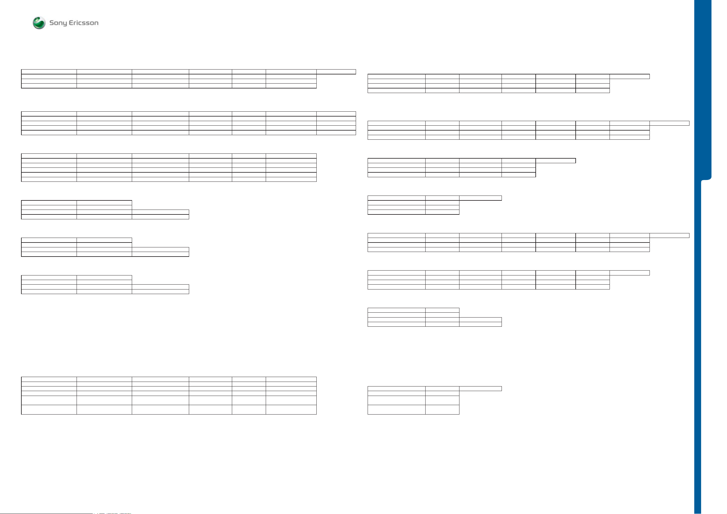
Battery and Current Calibration Test
Use the Phone with the ITP SW
Instrument settings for the Battery Calibration Test
Power Supply Channel 1 VBATT:
X Volt according to the Fault Trace SW Test Instructions:
Fault Trace SW-Logic-Phone Power-Battery Calibration and follow test instructions.
Limiter: 2A.
Power Supply Channel 2 DCIO/SEPI:
5.0 Volt
Limiter: 2A
If the test Is performed at the Core Level then use dummy battery according to the Equipment
List. If the TRS Fixture is used no dummy battery is needed.
Note: Maximal cable length between Power Supply Channel 1 VBATT and the dummy battery
or the TRS Fixture must be 1m. The cable must have a capacity for at least 16A.
Limits Table for the Battery Calibration Test
Voltage Level on VBATT Min Max UNIT
3.2 Volt
3.2 Volt
4.1 Volt
4.1 Volt
263 351 mV
107 15F HEX
789 877 mV
315 36D HEX
Backup Capacitor Test
To perform this test use:
- Phone with the ITP SW
- Power Supply Channel 1 VBATT: Instrument settings: Voltage: 3.8V, Limiter: 2A
- Power Supply Channel 2 DCIO/SEPI: Instrument settings Voltage: 5V, Limiter: 2A
This test should be preformed in 3 steps:
Step1:
Measure the voltage at the Backup capacitor by using Fault Trace SW- Logic - ADC Values –
Read ADC Value (Reading 1).
Step2:
This step should be done 30 seconds after Step 1. Measure the voltage at the Backup capacitor
by using Fault Trace SW - Logic – ADC Values - ADC Channels – Read ADC Value
(Reading 2).
Step3:
Compare the difference between Reading 1 and Reading 2 with the reference table below. If the
Reading 1 value is between 50 and 680 go to Interval 1, if between 681 and 800 go to Interval
2, if between 801 and 880 go to Interval 3 and compare with the Reading 2 – Reading 1 Min and
Max Limits.
TROUBLESHOOTING
Instrument settings for the Current Calibration Test
If the test is performed at the Core Level then use dummy battery according to the Equipment
List. If the TRS Fixture is used no dummy battery is needed.
Note: The Power Supply Channel 1 VBATT must allow reverse current.
Note: Maximal cable length between Power Supply Channel 1 VBATT and the dummy battery
or the TRS Fixture must be 1m. The cable must have a capacity for at least 16A.
Note: Length of the Power Supply Channel 2 DCIO/SEPI customized cable must be exactly
1,3m.
Power Supply Channel 1 VBATT:
3.8 Volt
Limiter 2A
Power Supply Channel 2 DCIO/SEPI:
5.0 Volt
Limiter: 2A
Limits Table for the Current Calibration Test
Measured Current Name Min Max Unit
100mA
800mA
DCIO Current 50 150 mA
DCIO Current 725 875 mA
Reference Table:
Min Max Unit
Absolute readout Reading 1 50 880 Dec
Reading 1 (Dec) Reading 2 – Reading 1 (Dec)
Min Max
Interval 1 (50 – 680) 20 210
Interval 2 (681 – 800) 5 30
Interval 3 (801 – 880) 0 10
Note: The upper table contains the absolute limits for the readouts. The lower table contains
the allowed delta between the first and the second readout, separated in time with 30 seconds.
If reading is out of the test limits then replace C2217 Backup capacitor.
If problem is not solved then SL 5 Replace N2000 SL 4 Escalate.
1215-3608 rev. 1
21 (96)
TROUBLESHOOTING
Charging Test - ASIC Revision Test
SEMC Troubleshooting Manual
K630 - V640 - K660
Charging Test
To perform this test use:
- Phone with the Normal SW (SSW)
- Dummy Battery connected to Power Supply Channel 1 VBATT
- Power Supply Channel 1 VBATT instrument settings:
Voltage: 3.0 to 4.2 Volts, according to VBATT row in the Reference Table.
Limiter: 2A
- Power Supply Channel 2 DCIO/SEPI instrument settings:
Voltage: 5V
Limiter: 2A
Test instructions:
- Disconnect the DCIO/SEPI Cable between each measurement and wait for phone to
shut down when changing VBATT voltage.
- Take a note of Current measurements at Power Supply Channel 2 DCIO/SEPI and
Display charging indicator status, X seconds after DCIO/SEPI cable has been inserted
according to Test Time row in the reference table below.
- Compare test results with the reference table below, tolerance +/-20%.
Reference Table
VBATT x Volt 3.0 3.1 3.2 3.3 3.4 3.5 3.6 3.7 3.8 3.9 4.0 4.1 4.2
Test Time x sec. 15s 15s 25s 25s 25s 25s 25s 25s 25s 25s 25s 25s 40s
DCIO/SEPI
Current mA
Display indicate
charging
220 220 200-400 200 200 200 200 770 770 770 700 430 0
Nothing Nothing Yes Yes Yes Yes Yes Yes Yes Yes Yes Yes
Fully
Charged
ASIC Revision Test
The purpose with this test is to check following items:
- that the ASICs Revision State is correct
- Check if communication to and from the ASIC-s is Ok
The following ASICs are tested:
- D2000 (Anja)
- N2000 (Vera)
- N1400 (Bluetooth and FM Radio ASIC)
To perform this test use:
- Phone with the ITP SW
- TRS Fixture
- Power Supply Channel 1 VBATT (Voltage: 3.8V, Limiter: 2A)
- Power supply Channel 2 DCIO/SEPI (Voltage: 5V, Limiter: 2A)
- Fault Trace SW choose General – Asic Revisions – Read All
Reference return value can be found in the table below.
TROUBLESHOOTING
Power Supply Channel 1 VBATT must allow
If the charging current is Not equal to the reference table go to Charging problems TRS
Guide.
If the charging current is equal to reference table then insert the normal battery and test the
charging current to define if the phone battery is working properly.
Measure the voltage at the battery to define the current level.
If the battery is receiving the right current, then the phone and the battery are working
properly.
reverse current.
ASIC Description Part Number Return Value (hex)
D2000 CPU (Anja) 1200-0186 0x2C8
N2000 Power Management (Vera) 1000-8142 0xC5
N1400 Bluetooth:
Firmware Revision
Chip ID
1200-6182
0x5,0x1
0x0,0x0,0x0,0x0
Will always return 0
on STLC because
Chip ID is not
supported.
N1400 FM Radio 1200-6182 0x800
1215-3608 rev. 1
22 (96)
TROUBLESHOOTING
V
o
V
h
V
o
A
V
a
A
V
V
oltages to N2000 WCDMA N1210
MP MP 92 (PBA GND) MP 63 (X2200 Pin 3) MP 89 (TP2200) MP 87 (TP2202) MP 26 (C2242) Power sup 3.80 V Use Fault Trace SW to activate and deactivate WCDMA Radi
Pnone Off 0.00V 3.8V 3.8V 0.00V 3.8V VCC_WPA WPAVCC DCDC_EN VccA VDDE18
Phone On 0.00V 3.8V 3.8V 0.00V 3.8V WCDMA Radio Off 0.00V 0.00V 0.00V 2.8V 1.8V
GND VBAT VBATI BDATA VDD_REF MP MP 56 (L2207) MP 54 (R2221) MP 55 (R2299) MP 36 (R2202) MP 33 (ST2208) Power sup 3.80 Volt
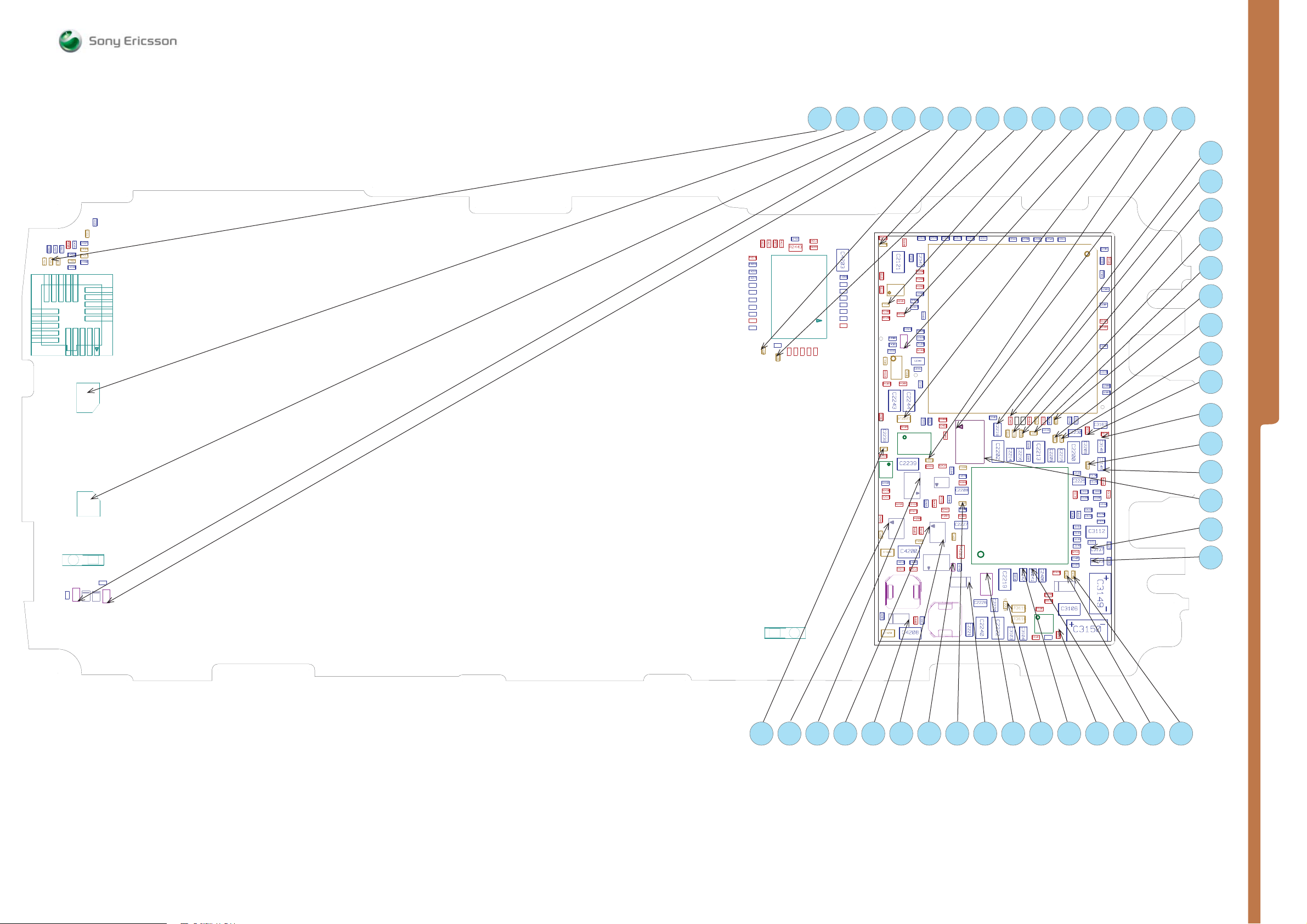
Reference Measurement Points
WCDMA Radio On 3.2V 1.3V 1.8V 2.8V 1.8V
SEMC Troubleshooting Manual
K630 - V640 - K660
oltages from N2000
MP MP 41 (ST2204) MP 34 (ST2203) MP 33 (ST2208) MP 37 (ST2212) MP 38 (ST2213) Bluetooth N1400
Phone Off 0.00V 0.00V 0.00V 0.00V 0.00V Power sup 3.80 Volt VDIG VDDE18 VBT27 VDDE18 BT_CLK RTCCLK
Phone On 2.6V 2.5V 1.8V 2.7V 2.7V Power sup 3.80 Volt Bluetooth Off 2.7V 1.8V 2.7V 1.8V 26MHz 32.768kHz
oltages from N2000 FM Radio N1400
MP MP 12 (ST2221) MP 36 (R2202) MP 31 (C2218) MP 52 (ST2210) Use Fault Trace SW to activate and deactivate FM Radi
Phone Off 0.00V 0.00V 2.2V 2.2V Power sup 3.80 Volt FM Radio Off 3.8V 1.8V 32.768kHz
Phone On 1.2V 2.8V 2.2V 2.2V Power sup 3.80 Volt FM Radio On 3.8V 1.8V 32.768kHz
Clocks to N2000 MP MP 35 (ST2202) Power sup 3.80 Volt
MP MP 43 (B2100_Pin7) VMC28
Phone Off 32.768kHz Power sup 0.00 Volt Phone On 2.8V
Phone On 32.768kHz Power sup 3.80 Volt
Clocks from N2000 MP MP 47 (R2280) MP 61 (TP2205) MP 59 (TP2206) MP 58 (TP2207) MP 11 (L4202) MP 84 (ST4312) Power sup 3.80 Volt
MP MP 22 (ST2105) CAM_LDO_EN VCAMSD13 VCAMSD28 VCAMSD18 CAMSYSCLK PCLK
Phone Off 0Hz Power sup 3.80 Volt Main Camera On 1.8V 1.3V 2.8V 1.8V 13MHz 19MHz
Phone On 32.768kHz Power sup 3.80 Volt
CORE18 from N2202 MP MP 47 (R2280) MP 59 (TP2206) MP 58 (TP2207) MP 11 (L4202) MP 1 (ST4314) Power sup 3.80 Volt
MP MP 15 (ST2217) CAM_LDO_EN VCAMSD28 VCAMSD18 CAMSYSCLK PCLK
Phone Off 0.00V Power sup 0.00 Volt VGA Camera On 1.8V 2.8V 1.8V 13MHz 19MHz
Phone On 1.8V Power sup 3.80 Volt
VAUDIO26 VANA25 VDDE18 VBT27 VDIG Use Fault Trace SW to activate and deactivate Bluetoot
0.00V 0.00V 0.00V 0.00V 0.00V Power sup 0.00 Volt MP MP 69 (ST1401) MP 66 (C1408) MP 73 (C1409) MP 64 (C1412) MP 10 (R2118) MP 22 (ST2105) Power sup 3.80 Volt
Bluetooth On 2.7V 1.8V 2.7V 1.8V 26MHz 32.768kHz
VCORE12 VccA VDD_LP VBACKUP MP MP 68 (C3304) MP 65 (C3305) MP 67 (R3301) Power sup 3.80 Volt
0.00V 0.00V 2.2V 2.2V Power sup 0.00 Volt VBATI VDDE18 RTCCLK
C2217 Completely charged
Memory Card
Memory Card inserted
RTCCLK Phone Off 0.00V
Main Camera
Use Fault Trace SW to activate and deactivate Main Camera. Main Camera must be connected to the PB
RTCCLK Main Camera Off 0.00V 0.00V 0.00V 0.00V 0Hz 0Hz
GA Camer
Use Fault Trace SW to activate and deactivate VGA Camera. VGA Camera must be connected to the PB
VCORE18 VGA Camera Off 0.00V 0.00V 0.00V 0Hz 0Hz
TROUBLESHOOTING
MCLK 26MHz from N1200
MP MP 9 (R2106)
Charging Phone On 26MHz Power sup 3.80 Volt
Charging off 1:
DCIO/SEPI not connected.
Charging off 2:
DCIO/SEPI connected.
MP MP 126 (C2201) MP 28 (C2241) MP 109 (V2202 Pin2) MP 106 (R2201) Power sup 3.8 Volt
Charging off 1 0.00V 3.6V 3.2V 3.8V Charger voltage 0.0 Volt MP MP 25 (ST2201) Power sup 3.80 Volt
Charging off 2 5.0V 4.7V 4.7V 3.8V Charger voltage 5.0 Volt VBUS
Charging 100mA 5.0V 4.8V 3.8V 3.8V Charger voltage 5.0 Volt
Charging 800mA 4.5V 4.3V 2.3V 4.2V Charger voltage 5.0 Volt
Charging 100mA: Use
Fault Trace SW:
Start Current Calibration----->
Set VBATT to 3.8
Note: The Current Calibration
Test must be repeted if current
consumtion going under 50mA
at Power Supply Channel 2
when you performing this
measurements.
DCIO DCIO_INT CHREG CHSENSEP USB cable connected to PC
Charging 800mA: Use
Fault Trace SW: Start
Current Calibration-->Set
VBATT to 3.8V-->Perform Step1
Note: The Current Calibration
Test must be repeted if current
consumtion going under 725mA
at Power Supply Channel 2 when
you performing this
measurements.
Phone Off 0Hz Power sup 3.80 Volt
BUS
USB Cable disonnected from the
phone
USB Cable connected to the
phone
MCLK
0.00V
5.0V
1215-3608 rev. 1
23 (96)
MEASUREMENT POINTS Front Side
SEMC Troubleshooting Manual
K630 - V640 - K660
MP 1 MP 2 MP 3 MP 4 MP 5 MP 6 MP 7 MP 8 MP 9 MP 10 MP 11 MP 12 MP 13 MP 14
MP 31
MP 32
C4328
Same net only Same net only
Same net only
Same net only
Same net only
Same net only
Same net only
C4317
C4327
ST4310
ST4314ST4316
Same net only
X4300
X1002
C31
41
R4305
C4332
ST4324
C4336
Same net only
y
Same net onl
C
4
C4325
32
6
ST4320
ST4318
C4330
y
Same net onl
Same net only
X3101
X3100
L3103
Same net only Same net only
ST43
17
Same net only
Same net only
Same net only
Same net
Same net
V3101
C
4
329
SP2107
ST2456
R2457
C2121
R21
21
R2
119
D2105
ST2106
R2100
R2120
C4302
C4301
C4316
ST4303 R4336
R4307
C2243
R2402
C2432
R4217
R4218
R4216
R4215
R4213
R4222
R4214
R2443
C4215
C4216
C4217
C4218
C4219
C4220
only
only
Same net only
C4221
C4222
R4221
C4214
25
X4200
1
C4213
ST4200
R4225
R4220
R421
ST4201
9
C4203
26
C4204
C4228
C4227
C4225
C4224
C4226
C4223
R4223
2
R4226
R4224
C2238
ST2217
R2435
N2400
C2430
R2438
R2437
R2436
R4208
V4206
ST4203
ST4202
C3142
L3104
V3102
X1001
L4201
C
4202
ST4250
V4201
R2220
R2101
R2118
C2324
L4202
S4300
ST4304
SP2102
R4308
C2244
ST2221
R2105
N2202
C2239
C4200
C4212 C4205
R4211 R4212
C4208
C2318
C2347
C2343
R1204
R1203
R1205
C2342
C2328
C2327
C2326
C2329
C5104
R2104
C2346
C2341
C2339
V2405
R2422
R2421
R4209
R4207
R4210
ST4204
R4202
C4201
C2316
C5
103
C2319 C2317
ST2216
R2222
R2439
C
2425
V4200
L2200
V2406
V4205
C2340 C2315 C2338 C2313
R2404
R2403
R2401
B2100
R2434
C21
ST2205
0
4
C4229
R2203
C2208
C
R2440
2204
ST2105
C2400
R2441
R4204
R2400
C2227
ST4207
R4203
C
L4200
4230
V2206
C2221
C2344 C2330
D2000
R2406
C2102
C2218
ST2208
ST2241
C2202
C2214
N2000
C2219
C2210
L2201
ST2201
C2220
C2226
ST3115
C2240
C2222
ST3116
C3103
C2336
C2311
C2345
ST2206
ST4313
R4309
R3134
C
2337
C3138
C2322
ST2203
C3155
ST2202
ST2213
ST2212
C2229
C2213
C2216
C2205
C2207
C2242
C3104
C2215
C2406
C2241
ST2401
R2419
V2400
R3102
R3110
R3106
C3106
N3100
R3137
R3103
C3105
C2314
C2335
R31
31
C2230
C2209
C2200
ST2204
C3136
C2225
R3135
C3167 C3165
C3168 C3166
C3133
C31
C31
2
27
6
C3132
C3152
C3139
C3135
C3140
R2416
C2405
C2429
ST2400
C3150
C3163
C3130
C3129
ST3114
C3112
C3151
C3137
C3123
C2301
R5
C2334
101
C2302
C2303
C2304
R2102
R2103
C2305
C2333
C2308
C2307
SP2106
R3130
C3146 C3145
R3132
R3133
C3164
C3134
C3128 C3102
C3149
MP 33
MP 34
MP 35
MP 36
MP 37
MP 38
MP 39
MP 40
MP 41
MP 42
MP 43
MP 44
MP 45
MEASUREMENT POINTS
MP 15 Mp 16 MP 17 MP 18 MP 19 MP 20 MP 21 MP 22 MP 23 MP 24 MP 25 MP 26 MP 27 MP 28 MP 29 MP 30
1215-3608 rev. 1
24 (96)
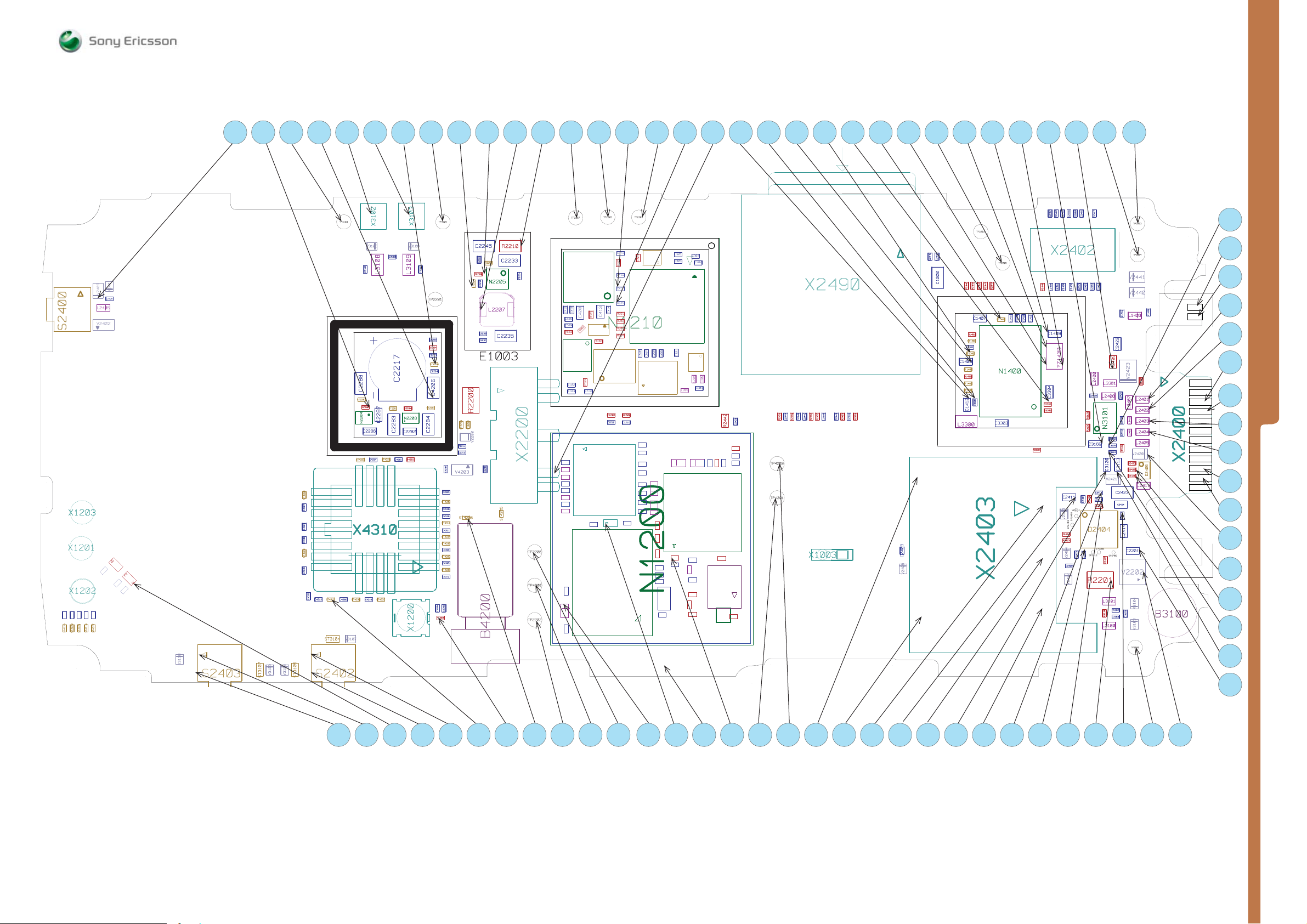
MEASUREMENT POINTS
Back Side
SEMC Troubleshooting Manual
K630 - V640 - K660
00
00
2244
SS
XX11220033
XX11220011
XX11220022
7
33
33
CC44
55
3322
TT44
S
S
SSTT44 332233 C4335C4335
SSTT44 332211 CC44 333333
MP 46 MP 47 MP 48 MP 49 MP 50 MP 51 MP 52 MP 53 MP 54 MP 55 MP 56 MP 57 MP 58 MP 59 MP 60 MP 61 Mp 62 MP 63 MP 64 MP 65 MP 66 MP 67 MP 68 MP 69 MP 70 MP 71 MP 72 MP 73 MP 74 MP 75 MP 76 MP 77
99
22
66
CC22446611
CC2244 55
CC2244664
CC2244 663
CC2244
XX2244002 2
5
44
2244
CC2244 665CC22446677
CC2244 668
CC2244 669
RR
CC11440099
ZZ11440000
CC33330044
RR33330033
RR33330022
CC22441111
SP2411
VV2244003
SP2409
SP2403
RR22442244
RR22442233
VV22440044
CC22440088
VV22440077
CC2244660
CC2244 7700
CC22442288
CC2244 5566CC2244 5577
CC22445588
CC22442200
RR33112299 RR33112288
CC33116699
66
4422
22
RR
CC22440077
DD22440044
SP2412
CC22441100
RR22220011
TP2207
N2001
C415
C416
C508
C509
R503
N3001
C102
C103
C1000
L1000
L1001
C1002
C1
00
3
L1002
C1016
L1004
C1015
L1006
C1014
C420
R502
R504
C510
R501
K401
R402
C1012
C418
Z301
R403
R405
C419
C417
C511
C414
R201
C413
R202
NN11221100
R203
R204
C506
K402
RR11220011
RR11220000
CC11221122
CC11221111
C1114
C1
1
13
C1110
C1109
Z1000
C
1
1
0
C
1
1
0
C
1
1
0
C
1
1
0
Z1001
C1013
N1002
N3000
C507
C204
C203
Z101
2
1
6
L1101 L1100
5
R1006
R1005
R1007
C
1
0
0
4
C
1
0
0
5
C
1
0
0
1
NN1122000 0
C1006
C101
7
C301
C304
R1000
C1020
S100
C201
L205
L1102
TP2203
88
C303
C302
XX22449900
Z201
L207
L206
C206
44
443
55
440
44
44
2244
224455 0CC22
RR2244 553
RR2244 5555
CC22
RR
CC2244 3311
RR22444422
R1
10
1
C1
1
N1001
19
C1118
C1117
R1100
C1116
R1105
B1100
R1
104
L1103
C1018
L1005
C1019
R1012
R1014
R1013
CC2244 4444RR
TP4200
TP4201
XX11000033
22
5511
4422
55
4455
44
22
CC2244 4411RR
CC2244
CC2244
RR2244
44
440044
44
CC22
CC22
CC11000000
CC11440088
SSTT11440055
RR11440000
SSTT11440022
SSTT11440066
LL33330000
TP2005
R2244446
RR2244 449
RR2244 4488
RR2244 447 7
RR2244 444 4
R
88
11
CC11440077
RR11440011
SSTT11440033
CC33330022
SSTT33330011
44
SSTT11440011
CC11441177
CC11
CC11441155
CC11441166
NN11440000
3333 0055
CC
CC11441122
CC33330033
RR33330044
CC2244009
VV2244008
XX2244003 3
VV22440099
LL22440066
TP3104 TP3105
VV22440011
CC2242266
XX3311002
VV33110055 VV33110066
CC33110088
LL33110088
XX33110033
CC22224455
CC33110099
CC33110077
LL33110099
TP2201
RR22221100
CC22223333
CC2222 3322
SSTT22222200
RR22229999
CC2222 3311
SSTT22 22222
NN22220055
44
33
22
CC22
LL22220077
VV22440022
CC22223366
CC22220033
RR22220044
CC22222233
SSTT22221100
CC22222244
CC22223355
CC22223377
E1003
CC22221177
CC222288 88
SSTT22228811
RR22228800
SSTT22228822
CC222288 77
NN22220044
CC22228866
CC222288 33
SSTT44332266
SSTT44332277 CC44331144
SSTT44 333300
CC44330077
CC4433 2200
CC44330066
6
006
1122
RR
0033
22
11
CC
220022
11
2
RR
002
2
112
CC
0011
22
11
CC
SSTT44 33119 C4333311C4
SSTT44 332222 CC4333344
VV331111 00
SS2244003 3
VV33110099
SSTT33110077
VV33110088
CC4433 2211 SSTT44332299
SSTT33110055
CC4433 2222
CC44331133 SSTT44331122
SS22440022
SSTT33110044
XX4433110 0
SSTT44333311 CC44331100 SSTT44333333
CC44330088
VV33110077
CC44331155 RR44330022
RR22228844
NN22220033
CC22228822
CC44220066
SSTT22228833
CC222288 4
RR22220000
4
4
2222
22223 3
22
22
SSTT
SSTT
VV22220000
CC22221111
CC22221122
XX2222000 0
CC4422007
CC44332233
SSTT44330066
CC44331199
CC44331188
SSTT44331111
CC44331111
SSTT44333344
SSTT44333322
CC44330099
SSTT44332288
CC44330055
SSTT44333355
CC44331122
CC1122004 4
CC1122000 0
RR11220088
XX11220000
VV44220033
SSTT44220066
CC2222 0066
SSTT442200 55
TP2200
TP4300
TP2202
BB44220000
TP2205
TP2206
MP 78
CC22442277
TP2003
TP2004
VV22444411
VV22444400
MP 110
MP 111
MP 112
MEASUREMENT POINTS
MP 113
CC11440011
LL11440033
CC11441133
MP 114
CC22442222
33
RR22440099
22
2244
VV
LL33330011
LL22440000
LL22440088
NN33110011
CC33112200
VV22442211
CC22441188
CC22441133
RR22442288
RR2244 0055
CC22442211
LL22440011
LL22440077
LL22440022
LL22440033
LL22440044
CC2244 1155 CC22441166
LL2244 0099 LL2244 1100
CC33111199
LL22440055
CC33112255
RR33111122
CC33112244
CC33111133
CC22442233
CC22442244
VV22442200
RR22443333
RR22443322
DD22440055
RR22443311
LL22441111
CC2244 1122
X2400
CC22441144
SP2404
CC22220011
SP2406
RR2244 2255
VV22220022
LL33110011
CC33116622
RR3311338
CC33116611
CC33116600
LL33110000
BB33110000
VV33110033 VV331100 44
TP3101
MP 115
MP 116
MP 117
MP 118
MP 119
MP 120
MP 121
MP 122
MP 123
MP 124
MP 125
MP 126
MP 79 MP 80 MP 81 MP 82 MP 83 MP 84 MP 85 MP 86 MP 87 MP 88 MP 89 MP 90 Mp 91 MP 92 MP 93 MP 94 MP 95 MP 96 MP 97 MP 98 MP 99 MP 100 MP 101 MP 102 MP 103 MP 104 MP 105 MP 106
MP 107 MP 108 MP 109
1215-3608 rev. 1
25 (96)
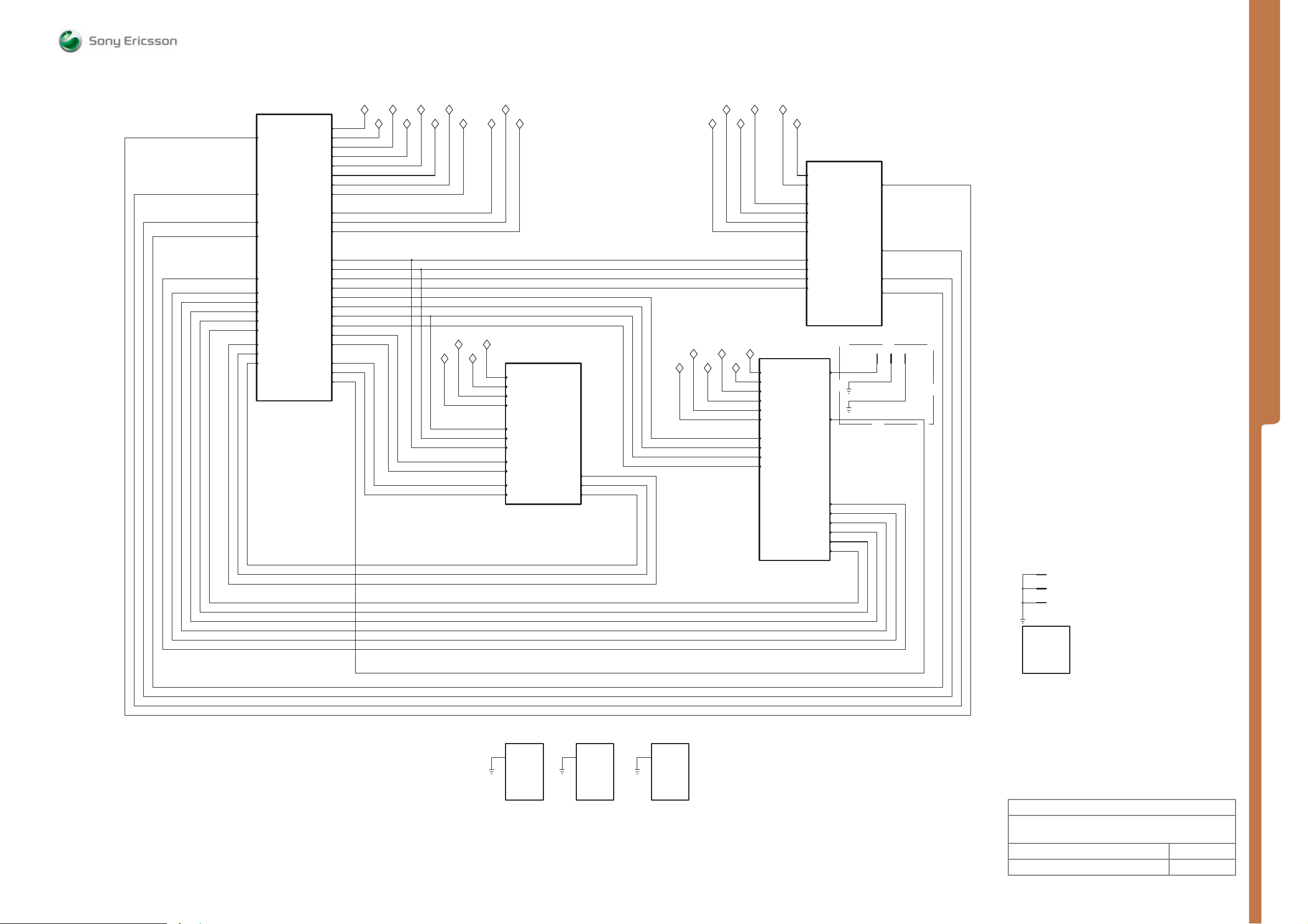
MEASUREMENT POINTS Top Schematic
SEMC Troubleshooting Manual
K630 - V640 - K660
KB_LED1
KB_LED2
VBOOST
VCC_WPA
KB_LED
KB_LED1
KB_LED2
MCLK
TX_ADSTR
DCDC_EN
TESTOUT
WPAVCC
BT_CLKREQ
VAD
SPL
SPR
Application & Sys.Performance
Application & Sys.Performance
VAUDIO26
VBEAR26
VCAMSD13
VCAMSD28
VCAMSD18
CAMSYSCLK
CAM_LDO_EN
MCLKREQ
MICN/AUXinR
MICP/AUXinL
FM_ANTENNA
VBATI
VDDE18
VDIG
VccA
VBT27
I2CCLK1
I2CDAT1
BT_CLK
RTCCLK
BTRESn
FMRESn
BT_ANT
VBATI VDIG VCC_WPA VAUDIO26
VDDE18 VccA VBEAR26 VCAMSD18VCAMSD13
VBT27
VBEAR26
I2CCLK1
I2CDAT1
CAMSYSCLK
MCLKREQ
BT_CLK
RTCCLK
BTRESn
VAUDIO26
VDDE18
MICN/AUXinR
MICP/AUXinL
FMRESn
FM_ANTENNA
VBATI
VCAMSD28
Audio
Audio
VBATI
VDDE18
VAUDIO26
VBEAR26
RTCCLK
I2CDAT1
I2CCLK1
MICN/AUXinR
MICP/AUXinL
FMRESn
FM_ANTENNA
CAM_LDO_EN
VAD
SPL
SPR
SPR
SPL
VAD
BT_CLKREQ
WPAVCC
TESTOUT
DCDC_EN
TX_ADSTR
MCLK
VBT27
VccA
VDDE18
VBATI
VDIG
VBATI
VDDE18
VccA
VCC_WPA
VBT27
VDIG
MCLKREQ
BT_CLK
RTCCLK
BTRESn
Access
Access
VDDE18
VBATIVCAMSD18 VCAMSD13
VBATI
VDDE18
VDIG
VCAMSD13
VCAMSD28
VCAMSD18
I2CCLK1
I2CDAT1
CAMSYSCLK
CAM_LDO_EN
Imaging
Imaging
ANT
BT_ANT
MCLK
TX_ADSTR
DCDC_EN
TESTOUT
WPAVCC
BT_CLKREQ
VBOOST
KB_LED
KB_LED1
KB_LED2
X1201 1 X1202 1 X1203
1
GSM/UMTS
KB_LED
X1003
X1001
X1002
MEASUREMENT POINTS
1
1
1
VCAMSD28
VCC_WPAVDIG
BT_ANT
VBOOST
E1001
Clamp
1
GND
Will be connected
to GND in PCB
BB1_FENCE_SANIA
1200-7601 1200-7604 1200-7603
E1002
Clamp
1
GND
Will be connected
to GND in PCB
BB2_FENCE_SANIA
1
E1003
Clamp
GND
Will be connected
to GND in PCB
BB1_FENCE_SANIA
Test
Made for
Top Schematic
Document Nr Revision
1201-2734 Page 1
1215-3608 rev. 1
6
26 (96)
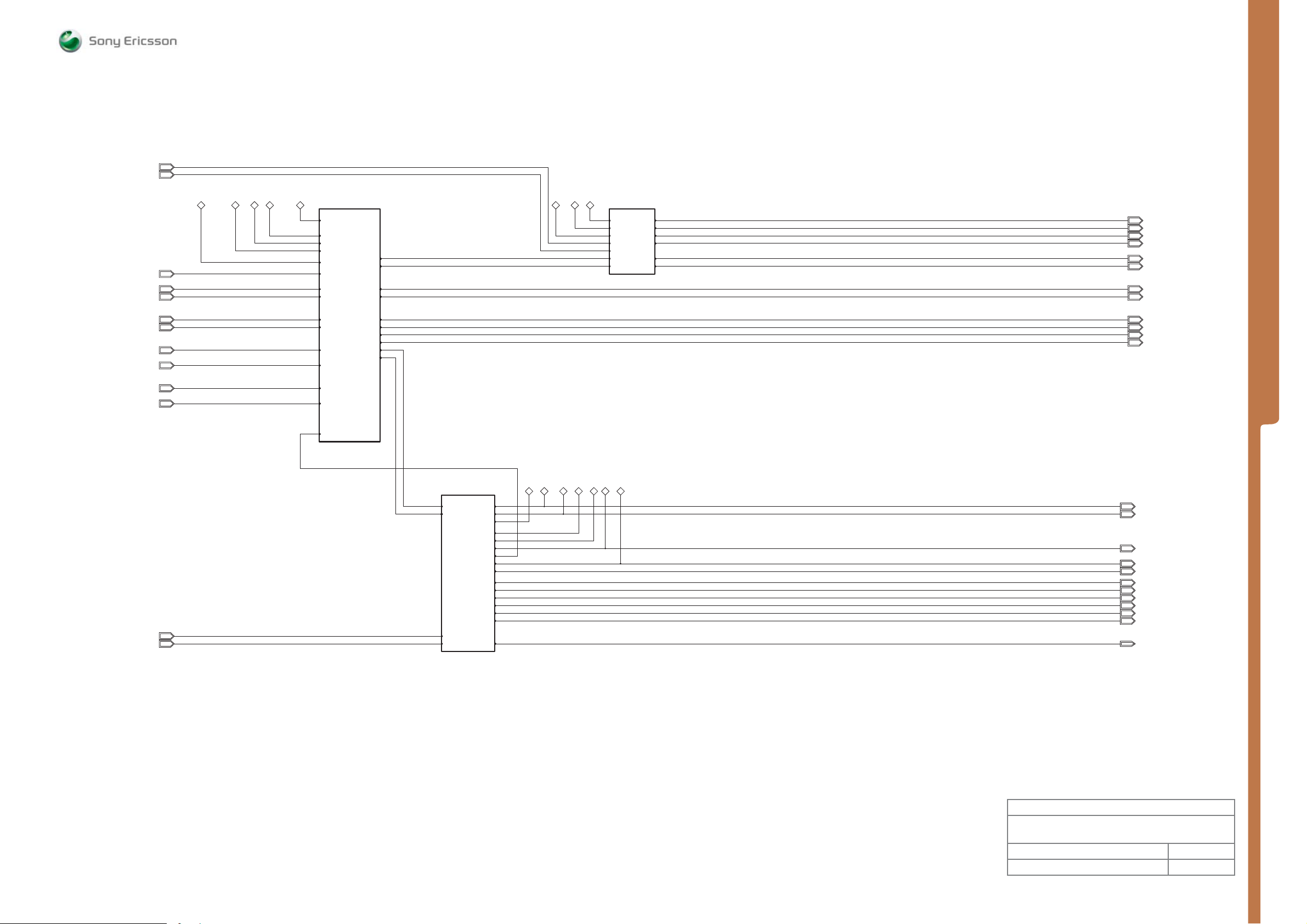
MEASUREMENT POINTS
Application & Syste m Perfor ma n ce Top
SEMC Troubleshooting Manual
K630 - V640 - K660
BT_CLKREQ
MCLK
TESTOUT
VAD
TX_ADSTR
SPL
SPR
VBOOST
KB_LED
KB_LED1
KB_LED2
WPAVCC
DCDC_EN
VDDE18_ANJA
VAUDIO26
TESTOUT
VAD
TX_ADSTR
SPL
SPR
VBOOST
KB_LED
KB_LED1
KB_LED2
VMC18
VDDE18
VBATI
VBATI
VDDE18
VMC18
VAUDIO26
VDDE18_ANJA
TESTOUT
VAD I2CDAT1
TX_ADSTR I2CCLK1
SPL
SPR
VBOOST
KB_LED
KB_LED1
KB_LED2
VBACKUP
Connectivit y
Connectivit y
SERVICEn
ONSWAn
MICN/AUXinR
MICP/AUXinL
FM_ANTENNA
BT_ANT
VBACKUP
VBUS
DCIO
VBUS
DCIO
WPAVCC
DCDC_EN
BT_CLKREQ
MCLK
VDDE18
VDDE18_ANJA
SERVICEn
ONSWAn
I2CDAT1 I2CDAT1
I2CCLK1 I2CCLK1
MICN/AUXinR
MICP/AUXinL
FM_ANTENNA
BT_ANT
VDDE18_ANJA
VBATI
VBUS
DCIO
WPAVCC
PowerPower
VBATI
VDDE18
VDDE18_ANJA
VDD_LP
VMC18
VDIG
VBACKUP
VAUDIO26
VBEAR26
VCAMSD13
VCAMSD28
VCAMSD18
VBT27
VccA
VCC_WPA
CAD_LDO_ENDCDC_EN
VDDE18
VDD_LP
VDD_LP
VMC18
VDD_LP
VDDE18
VDDE18_ANJA
MCLK
SERVICEn
ONSWAn
System ControlSystem Control
VDIG
VAUDIO26
CAMSYSCLK
MCLKREQBT_CLKREQ
VBATI
VDDE18
VDIG
VAUDIO26
VBEAR26
VCAMSD13
VCAMSD28
VCAMSD18
VBT27
VccA
VCC_WPA
CAM_LDO_EN
RTCCLK
BT_CLK
BTRESn
FMRESn
RTCCLK
BT_CLK
CAMSYSCLK
MCLKREQ
BTRESn
FMRESn
FM_ANTENNA
RTCCLK
BT_CLK
CAMSYSCLK
MCLKREQ
BTRESn
FMRESn
I2CDAT1
I2CCLK1
MICN/AUXinR
MICP/AUXinL
FM_ANTENNA
BT_ANT
VBATI
VDDE18
VDIG
VAUDIO26
VBEAR26
VCAMSD13
VCAMSD28
VCAMSD18
VBT27
VccA
VCC_WPA
CAM_LDO_EN
MEASUREMENT POINTS
Made for
Application & System Performance
Performance & Applications Top
Document Nr Revision
1201-2734 Page 2
1215-3608 rev. 1
6
27 (96)
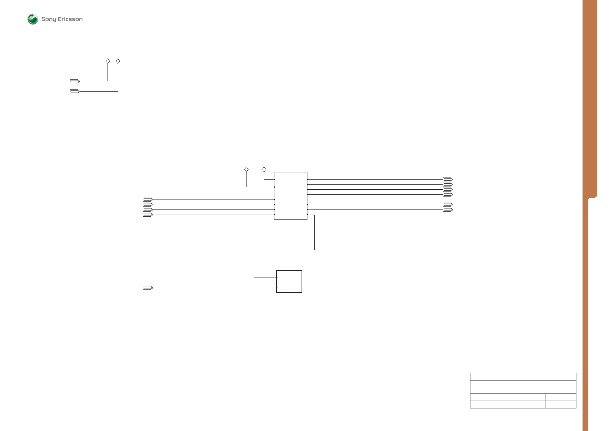
VDDE18
VDD_LP
VDDE18 VDD_LP
MEASUREMENT POINTS System Top
SEMC Troubleshooting Manual
K630 - V640 - K660
MEASUREMENT POINTS
BT_CLKREQ
MCLK
SERVICEn
ONSWAn
VDDE18_ANJA
BT_CLKREQ
MCLK
SERVICEn
ONSWAn
VDDE18_ANJA
VDD_LP
VDDE18
VDDE18
VDD_LP
BT_CLKREQ
MCLK
SERVICEn
ONSWAn
Clocks & Resets
MEMRESn
MEMRESn
VDDE18_ANJA
MemoriesMemories
BT_CLK
CAMSYSCLK
RTCCLK
MCLKREQ
BTRESn
FMRESn
MEMRESn
BT_CLK
CAMSYSCLK
RTCCLK
MCLKREQ
BTRESn
FMRESn
BT_CLK
CAMSYSCLK
RTCCLK
MCLKREQ
BTRESn
FMRESn
Made for
Application & System Performance
System Top
Document Nr Revision
1201-2734 Page 3
1215-3608 rev. 1
6
28 (96)
MEASUREMENT POINTS Syste m Co nt rol - Clo cks & Re set s
SEMC Troubleshooting Manual
K630 - V640 - K660
VDDE18
VDD_LP
MCLK
BT_CLKREQ
SERVICEn
ONSWAn
VDDE18 VDD_LP
R2100
120Kohms
C2104
1nF
PWRRSTn
MP 22
ST2105
VDDE18 VDDE18
R2119
100Kohms
C2121
4.7uF
MCLK
RTCCLK
BT_CLKREQ
SERVICEn
ONSWAn
N2000
Ericsson AB 3100
SYSTEM CONTROL
SYSTEM POR
E13
IRQA_N
E14
IRQB_N
E12
PWRRST_N
12
11B
XTAL_OUT
Strap
AB3100
1000-8142
R2121
10ohms
MP 9
VDD_LP
CLOCK
RTC
ST2106
Strap
2 1
ONSWA_N
ONSWB_N
ONSWC
XTAL1
XTAL2
SLEEP_A
SLEEP_B
MCLK
1A
A
AB17
A
AE22
AD22
T
AD19
F13
F12
F11
A
D11
E11
D14
H13
61B
81B
31
01
D2105
1
OE
2
5 3
D2000
MCLK
RTCCLKIN
SYSCLK0REQn
MSACCIRQn
MSAPPIRQn
PWRRSTn
SERVICEn
ANJA-Bottom
1200-0186
0.001uF
C2203
SP2106 SP2107
Y
A
VCC
GND
SN74LVC1G125YZPR
1200-0425
Anja-PoP bottom - SYSTEMLEVEL
CLOCKS
INTERRUPTS
RESETS
POWER CONTROL
2
0.1uF
3
4
C2102
5
6
4
1A
MCLKREQ
RESOUT0n
RESOUT1n
RESOUT2n
ACCSLEEP
APPSLEEP
B2100
VIO
NC_2
NC_3
NC_4
NC_5
GND VCC
SG-3030LC
1200-3231
DCON
Strap
2 1
ST2205
PWRREQn
SYSCLK0
SYSCLK1
SYSCLK2
DCON
OUT
NC_8
NC_9
NC_10
NC_11
R2101
100Kohms
1CA
AC18
A
AB19
AE18
AD18
AB20
AD17
AB23
1A
MP 43 MP 14
71
8
9
10
11
12
R2118
68ohms
R2120
0ohms
<NM>
RTCCLK
BT_CLK
RTCCLK
BT_CLK
MP 10
MEASUREMENT POINTS
6
71C
SP2102
32CA
R2104
47ohms
R2105 100Kohms
D2000
V5
ACCESS GPIO_16
ANJA-Bottom
1200-0186
MCLKREQ
CAMSYSCLK
MEMRESn
FMRESn
BTRESn
1A
MCLKREQ
CAMSYSCLK
MEMRESn
FMRESn
BTRESn
Made for
Application & System Performance
System Control - Clocks & Resets
Document Nr Revision
1201-2734 Page 4
1215-3608 rev. 1
6
29 (96)
 Loading...