

Page 1
SD Card Specification
Simplified Version of:
Part E1
SD Input/Output (SDIO)
Card Specification
Version 1.00
October, 2001
SD Association
Copyright 2000, 2001 SD Association
Page 2
SDIO Simple Specification Version 1.0 DO NOT COPY ©Copyright SD Association, 2000, 2001
Revision History
Date Version Changes compared to previous issue
October, 2001 1.0 Base version initial release
Conditions for publication
Publisher and Copyright Holder:
SD Association
719 San Benito St. Suite C
Hollister, CA 95023
USA
Phone: +1 831 636 7322
Fax: +1 831 623 2248
E-mail: [email protected]
Confidentiality:
This document is a simplified version of the original. This version is not required to be treated as confidential
and Non Disclosure Agreement with neither the 3C LLC nor the SDA is required.
Reproduction in whole or in part is prohibited without prior written permission of SDA.
Exemption:
None will be liable for any damages from use of this document.
Important additional information!
The reader is directed to the additional information available in section Error! Reference source not found..
This information will inform the reader of changes to the SDIO specification proposed for the next revision of
this specification that should be considered in the design of any SDIO device.
l
Page 3

SDIO Simple Specification Version 1.0 DO NOT COPY ©Copyright SD Association, 2000, 2001
Table of Contents
1. General Description.................................................................................................................................... 1
1.1 SDIO features ..................................................................................................................................... 1
1.2 Primary Reference Document ............................................................................................................. 1
2. SDIO Signaling Definition ........................................................................................................................... 2
2.1 SDIO Card Types................................................................................................................................ 2
2.2 SDIO Card modes............................................................................................................................... 2
2.2.1 SPI (Card mandatory support) ..................................................................................................... 2
2.2.2 1-bit SD data transfer mode (Card mandatory support) ............................................................... 2
2.2.3 4-bit SD data transfer mode (mandatory for High-Speed cards, optional for Low-Speed) ........... 2
2.3 SDIO Host Modes ............................................................................................................................... 2
2.4 Signal Pins .......................................................................................................................................... 3
2.5 Host Requirements for SDIO............................................................................................................... 3
3. SDIO Card Initialization .............................................................................................................................. 4
3.1 Differences in I/O card initialization ..................................................................................................... 4
4. Differences with SD Memory Specification................................................................................................. 7
4.1 Unsupported SD Memory commands ................................................................................................. 7
4.2 Bus Width............................................................................................................................................ 8
4.3 Card Detect Resistor........................................................................................................................... 8
4.4 Data Transfer Abort............................................................................................................................. 8
4.5 Changes to SD Memory Fixed Registers ............................................................................................8
4.5.1 OCR Register............................................................................................................................... 8
4.5.2 CID Register................................................................................................................................. 8
4.5.3 RCA Register ............................................................................................................................... 8
5. New I/O Read/Write Commands ................................................................................................................ 9
5.1 IO_RW_DIRECT command (CMD52)................................................................................................. 9
5.2 IO_RW_EXTENDED command (CMD53)........................................................................................... 9
5.2.1 CMD53 Data Transfer Format......................................................................................................9
6. SDIO Card Internal Operation .................................................................................................................. 10
6.1 Overview ........................................................................................................................................... 10
6.2 Register Access Time ....................................................................................................................... 10
6.3 Interrupts ........................................................................................................................................... 10
6.4 Suspend/Resume...............................................................................................................................11
6.5 Read Wait (Optional)..........................................................................................................................11
6.6 SDIO Fixed Internal Map................................................................................................................... 12
6.7 Common I/O Area (CIA) .................................................................................................................... 12
6.8 Card Common Control Registers (CCCR)......................................................................................... 13
6.9 Function Basic Registers (FBR) ........................................................................................................ 13
6.10
6.11
6.12
7. SDIO Interrupts ........................................................................................................................................ 14
7.1 Interrupt Timing ................................................................................................................................. 14
7.1.1 SPI and SD 1-bit mode interrupts............................................................................................... 14
7.1.2 SD 4-bit mode ............................................................................................................................ 14
7.1.3 Interrupt Clear Timing................................................................................................................. 14
8. SDIO Physical Properties ......................................................................................................................... 15
8.1 SDIO Size ......................................................................................................................................... 15
8.2 SDIO Card Package.......................................................................................................................... 15
9. SDIO Mechanical Extensions ................................................................................................................... 16
9.1 Additional ESD/EMI Ground Point..................................................................................................... 16
9.2 Extended Case.................................................................................................................................. 16
9.3 Write Protect Switch.......................................................................................................................... 16
10. SDIO Power.......................................................................................................................................... 18
10.1
Card Information Structure (CIS) ................................................................................................... 13
Multiple Function SD Cards ........................................................................................................... 13
Embedded I/O Code Storage Area (CSA) ..................................................................................... 13
SDIO Card Initialization Voltage .................................................................................................... 18
i
Page 4

SDIO Simple Specification Version 1.0 DO NOT COPY ©Copyright SD Association, 2000, 2001
10.2
10.3
11. Abbreviations and Terms ...................................................................................................................... 19
A.1 SD and SPI Command List .....................................................................................................................A
B.1 Normative References ............................................................................................................................C
C.1 Example SDIO Controller Design ...........................................................................................................D
SDIO Power Consumption............................................................................................................. 18
SDIO Current................................................................................................................................. 18
Table of Tables
Table 1 SDIO pin definitions .............................................................................................................................. 3
Table 2 Unsupported SD Memory Commands .................................................................................................. 7
Table 3 SDIO exceptions to SD physical section 8.1 requirements .................................................................15
Table 4 SD Mode Command List....................................................................................................................... A
Table 5 SPI Mode Command List ...................................................................................................................... B
Table of Figures
Figure 1 Signal connection to two 4-bit SDIO cards .......................................................................................... 3
Figure 2 Card initialization flow in SD mode (SDIO aware host)........................................................................ 5
Figure 3 Card initialization flow in SPI mode (SDIO aware host)....................................................................... 6
Figure 4 SDIO Internal Map............................................................................................................................. 12
Figure 5 SDIO Mechanical Extensions ............................................................................................................ 17
Figure 6 SDIO Internal State Machine example ................................................................................................D
Figure 7 State Diagram for Bus State Machine .................................................................................................D
Figure 8 State Diagram for Function State Machine.......................................................................................... E
ii
Page 5

SDIO Simple Specification Version 1.0 DO NOT COPY ©Copyright SD Association, 2000, 2001
1. General Description
The SDIO (Secure Digital I/O) card is based on and compatible with the SD memory card. This compatibility
includes mechanical, electrical, power, signaling and software. The intent of the SDIO card is to provide
high-speed data I/O with low power consumption for mobile electronic devices. A primary goal is that an SDIO
card inserted into a non-SDIO aware host will cause no physical damage or disruption of that device or it’s
software. In this case, the SDIO card should simply be ignored. Once inserted into an SDIO aware host, the
detection of the card will be via the normal means described in the SD specification with some extensions. In
this state, the SDIO card will be idle and draw a small amount of power (15 mA averaged over 1 second).
During the normal initialization and interrogation of the card by the host, the card will identify itself as an SDIO
device. The host software will then obtain the card information in a tuple (linked list) format and determine if
that card’s I/O function(s) are acceptable to activate. This decision will be based on such parameters as power
requirements or the availability of appropriate software drivers. If the card is acceptable, it will be allowed to
power up fully and start the I/O function(s) built into it.
1.1 SDIO features
z Targeted for portable and stationary applications
z Minimal or no modification to SD Physical bus is required
z Minimal change to memory driver software
z Extended physical form factor available for specialized applications
z Plug and play (PnP) support
z Multi-function support including multiple I/O and combined I/O and memory
z Up to 7 I/O functions plus one memory supported on one card.
z Allows card to interrupt host
z Initialization Voltage: 2.0 to 3.6V
z Operational Voltage range: 3.1 to 3.5V
1.2 Primary Reference Document
This spec is based on and refers extensively to the SDA document:
SD Memory Card Specifications
Part 1
PHYSICAL LAYER SPECIFICATION
September 2000
Version 1.01
The reader is directed to this document for more information on the basic operation of SD devices. In addition,
other documents are referenced in this specification. A complete list can be found in section B.1.
1
Page 6

SDIO Simple Specification Version 1.0 DO NOT COPY ©Copyright SD Association, 2000, 2001
2. SDIO Signaling Definition
2.1 SDIO Card Types
This specification defines two types of SDIO cards. The Full-Speed card supports SPI, 1-bit SD and the 4-bit
SD transfer modes at the full clock range of 0-25MHz. The Full-Speed SDIO devices have a data transfer rate
of over 100 Mb/second (10 MB/Sec). A second version of the SDIO card is the Low-Speed SDIO card. This
card requires only the SPI and 1-bit SD transfer modes. 4-bit support is optional. In addition, Low-Speed SDIO
cards shall support a full clock range of 0-400 KHz. The intended use of Low-Speed cards is to support
low-speed IO devices with a minimum of hardware. The Low-Speed cards support such functions as modems,
bar-code scanners, GPS receivers etc. If a card is a ‘Combo card’ (memory plus SDIO) then Full-Speed and
4-bit operation is mandatory for both the memory and SDIO portions of the card.
2.2 SDIO Card modes
There are 3 signaling modes defined for SD physical specification version 1.01 memory cards that also apply
to SDIO Card:
2.2.1 SPI (Card mandatory support)
The SPI bus topology is defined in section 3.1.2 and the protocol is defined in sections 3.2.2 and 7 of the
SD Memory Card Specifications, PHYSICAL LAYER SPECIFICATION, Part 1,September 2000 Version
1.01. In this mode pin 8, which is undefined for memory, is used as the interrupt pin. All other pins and
signaling protocols are identical to the SD Memory specification.
2.2.2 1-bit SD data transfer mode (Card mandatory support)
This mode is identical to the 1 data bit (narrow) mode defined for SD Memory in section 3.2.1 of the SD
Memory Card specification. In this mode, data is transferred on the DAT[0] pin only. In this mode pin 8,
which is undefined for memory, is used as the interrupt pin. All other pins and signaling protocols are
identical to the SD Memory specification.
2.2.3 4-bit SD data transfer mode (mandatory for High-Speed cards, optional for Low-Speed)
This mode is identical to the 4 data bit mode (wide) defined for SD Memory in section 3.2.1 of the SD
Memory Card specification. In this mode, data is transferred on all 4 data pins (DAT[3:0]). In this mode the
interrupt pin is not available for exclusive use as it is utilized as a data transfer line. Thus, if the interrupt
function is required, a special timing is required to provide interrupts. See section 7.1.2 for details of this
operation. The 4-bit SD mode provides the highest data transfer possible, up to 100 Mb/sec.
2.3 SDIO Host Modes
If a SDIO aware host supports the SD transfer mode, it is recommended that both the 1-bit and 4-bit modes be
supported. While a SDIO host that supports only the 4-bit transfer mode is possible, it’s performance with a
Low-Speed SDIO card would be reduced. This is because the only means to transfer data to and from a
Low-Speed card would be the single byte per command transfer (using the IO_RW_DIRECT command
(CMD52) see 5.1).
2
Page 7
SDIO Simple Specification Version 1.0 DO NOT COPY ©Copyright SD Association, 2000, 2001
2.4 Signal Pins
CLK
CMD
DAT[3:0]
SD Host
CLK
CMD
DAT[3:0]
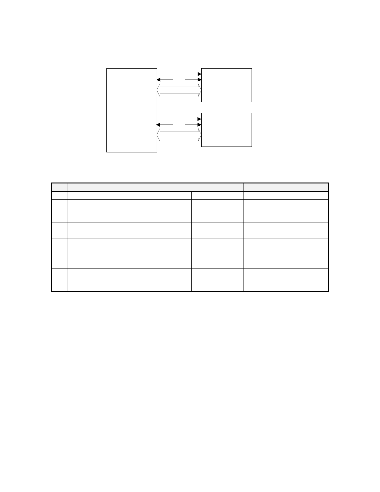
Figure 1 Signal connection to two 4-bit SDIO cards
Pin SD 4-bit mode SD 1-bit mode SPI mode
1 CD/DAT[3] Data line 3 N/C Not Used CS Card Select
2 CMD Command line CMD Command line DI Data input
3 VSS1 Ground VSS1 Ground VSS1 Ground
4 VDD Supply voltage VDD Supply voltage VDD Supply voltage
5 CLK Clock CLK Clock SCLK Clock
6 VSS2 Ground VSS2 Ground VSS2 Ground
7 DAT[0] Data line 0 DATA Data line DO Data output
8 DAT[1] Data line 1 or
IRQ Interrupt IRQ Interrupt
Interrupt
(optional)
9 DAT[2] Data line 2 or
RW Read Wait
Read Wait
(optional)
SD I/O Card
SD I/O Card
NC Not Used
(optional)
It is recommended that multi-slot hosts intending to support SDIO (SDIO aware) provide a separate CLK to
each slot, to allow the I/O devices to be placed in a low power state on a slot-by-slot basis. After reset, all data
lines (DAT[3:0]) shall be in the hi-Z state on both the host and card(s) to avoid bus conflict. Access to the Bus
Interface Control register within the CCCR determines DAT line mode.
2.5 Host Requirements for SDIO
In order for a host to completely support all of the capabilities of the SDIO cards, some signal connections
must be supported. In order to support interrupts, the host shall have Pin 8 connected from the card to the host
in order to provide interrupt signaling. This is true even if the host will only support the SPI or 1 bit SD mode. In
addition, if the host supports more than 1 card in either SD mode, the CMD and all 4 data lines (DAT[3:0])
should not be bussed together, but rather routed separately to the host. This will allow the mixing of card types
in the different sockets without interference. Both the SD Memory specification and the SDIO specification
support the concept of “unifying” (connecting together) the CMD lines in a multi-slot system after initialization.
3
Table 1 SDIO pin definitions
Page 8

SDIO Simple Specification Version 1.0 DO NOT COPY ©Copyright SD Association, 2000, 2001
3. SDIO Card Initialization
3.1 Differences in I/O card initialization
A requirement for the SDIO specification is that an SDIO card must not cause non-I/O aware hosts to fail when
inserted. In order to prevent operation of I/O Functions in non-I/O aware hosts, a change to the SD card
identification mode flowchart is needed. A new command (IO_SEND_OP_COND, CMD5) is added to replace
the ACMD41 for SDIO initialization by I/O aware hosts.
After reset or power-up, all I/O functions on the card are disabled and the I/O portion of the card will not
respond to any operation except CMD5 or CMD0 with CS=low. If there is SD memory installed on the card
(also called a combo card), that memory will respond normally to all normal mandatory memory commands.
An I/O only card will not respond to the ACMD41 and thus appear initially as an MMC card (See B.1 for
information on the MMC specification). The I/O only card will also not respond to the CMD1 used to initialize
the MMC cards and appear as a non-responsive card. The host will then give up and disable this device Thus,
the non-aware host will receive no response from an I/O only card and force it to the inactive state.
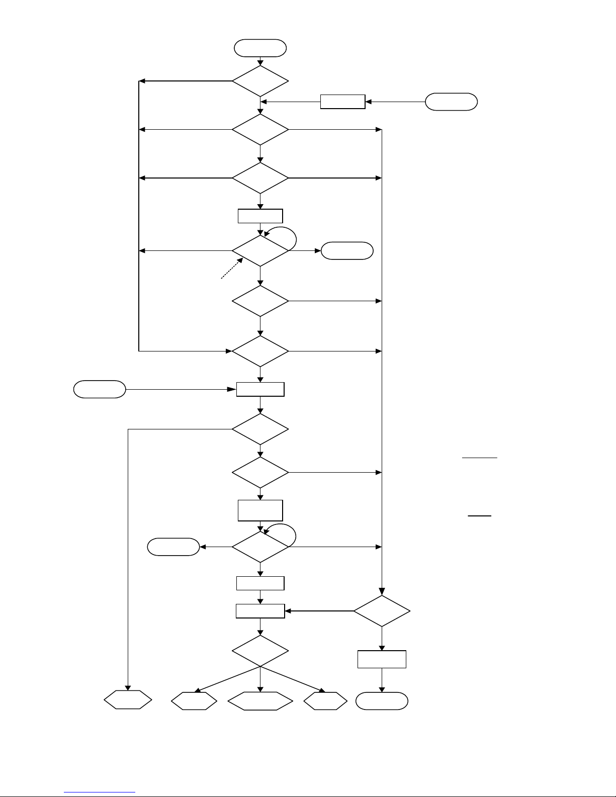
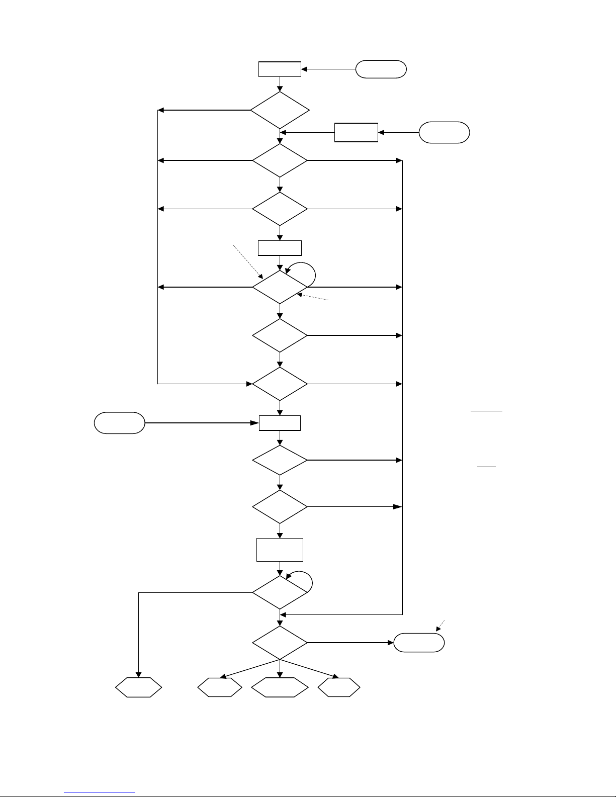
An SDIO aware host will send CMD5 prior to the CMD55/ACMD41 pair, and thus would receive a valid OCR in
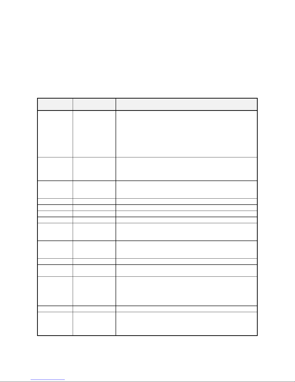
the R4 response to CMD5 and continue to initialize the card. Figure 2 shows the operation of an SDIO aware
host operating in the SD modes and Figure 3 shows the same operation for a host that operates in the SPI
mode.
If the I/O portion of a card has received no CMD5, the I/O section remains inactive and will not respond to any
command except CMD5. A combo card stays in the memory-only mode. If no memory is installed on the card
(i.e. an I/O only card in a non-SDIO aware host) the card would not respond to any memory command. This
satisfies the condition where a user uses some I/O function on the card such as Ethernet to load a music file to
the memory function of that card. The card is then removed and inserted into a non-SDIO aware host. That
device would not enable the I/O function (no CMD5) so would appear to the player as a memory-only card. If
the host were I/O aware, it would send the CMD5 to the card and the card would respond with R4. The host
reads that R4 value and knows the number of available I/O functions and about the existence of any SD
memory.
The function of CMD5 for SDIO cards is similar to the operation of ACMD41 for SD memory cards. It is used to
inquire about the voltage range needed by the I/O card. The normal response to CMD5 is R4 in either SD or
SPI format. The I/O aware host will send CMD5. If the card responds with response R4, the host determines
the card’s configuration based on the data contained within the R4.
After the host has initialized the I/O portion of the card, it then reads the Common Information Area (CIA) of the
card (see 6.7). This is done by issuing a read command, starting at byte 00 of I/O function 0. The CIA contains
the Card Common Control Registers (CCCR) and the Function Basic Registers (FBR). Also included in the
CIA are pointers to the card’s common Card Information Structure (CIS) and each individual function’s CIS.
The CIS includes information on power, function, manufacturer and other things the host needs to determine if
the I/O function(s) is appropriate to power-up. If the host determines that the card should be activated, a
register in the CCCR area enables the card and each individual function. At this time, all functions of the I/O
card are fully available. In addition, the host can control the power consumption and enable/disable interrupts
on a function-by-function basis. This access to I/O will not interfere with memory access to the card if present.
4
Page 9
SDIO Simple Specification Version 1.0 DO NOT COPY ©Copyright SD Association, 2000, 2001
Power ON
{IO=0, MEM=0, PI=0}
No
Init IO ?
Yes
CMD52
I/O R es et
{IO=0 }
Rein it IO
Rein it
Memory
if NR or (F=0 & MP=1)
if O C R in va lid & M P=1
IORDY tim eout
indicate s IO failu re
{M EM =0 }
if timeout
CMD5
arg=0
if F> 0
Test IO
OCR
OCR valid
Set new
Voltage
CMD5
arg=WV
if IORDY=1
(IO=1 )
Test
MP
if PI=0 and MP=1
Init
Memory?
Yes
CMD0
if F= 0 & M P = 0
if O C R in va lid & M P=0
IORDY=0
Inactive State
if N R
if PI=1 or M P = 0
No
MMC
Card
M P=0 , IO =0
Start initia liz atio n
with CMD0, CMD1
Inactive State
Mem
only
IO =0 , M E M = 1
if N R
if N R
ACMD41
arg=00
Get mem
OCR
Test mem
OCR
mem OCR valid
Set new
Voltage
(if needed)
ACMD41
arg=WV
if MEMRDY
(M EM =1)
CMD2
CMD3
{PI= 1 }
Test flags
Combo
IO =1 , M E M = 1
if mem OCR
inv alid
MEMRDY=0
if MEM RD Y timeout
IO or MEM=1
I/O
only
IO =1 , M E M = 0
F:
NR:
IO R D Y :
bit in the response CMD5)
MRDY:
rea dy (Bit31 o f O C R )
IO :
MEM:
MP:
PI:
IR:
Test flags
IO =0,M EM = 0
CMD15
Inactive State
Variables
Num ber o f IO fu n ctio n s
No Response
I/O Power-up status is ready (C
Mem ory power-up status is
Flags
I/O F unctio n s initia lized fla g
M e m o ry in itia liz e d fla g
Memory exists flag (in the
response of CMD5)
Pow e r O n In itia lizatio n
Illegal comm and Response
Figure 2 Card initialization flow in SD mode (SDIO aware host)
5
Page 10
SDIO Simple Specification Version 1.0 DO NOT COPY ©Copyright SD Association, 2000, 2001
{IO=0, MEM=0, PI=0}
CMD0 +
CS=low
Power ON
No
if IR or (F=0 & MP=1)
if OCR invalid & MP=1
No voltage
compare
performed by card
for CMD5
if (IR or timeout)
& MP=1
if PI=0 and MP=1
Yes
Set new
arg=WV
if IORDY
(IO=1)
Memory?
Init IO?
CMD5
arg=0
if F>0
Test IO
OCR
OCR Valid
Voltage
CMD5
Test
MP
Init
CMD52 IO
Reset
if (F=0 & MP=0)
if OCR invalid & MP=0
IORDY=0
if (IR or timeout)
& MP=0
IORDY timeout
indicates IO failure
if PI=1 or MP=0
No
{IO=0}
Reinit IO
MMC
Card
{MEM=0}
Reinit
Memory
IO=0, MEM=0
Start initialization with
CMD0 and CMD1
Get MemoryOCR
if MEMRDY MEM=1
IO=0,MEM=1
Mem
only
if IR
Test Mem
OCR Valid
Set new
(if needed)
ACMD41
arg=WV
IO=1,MEM=1
Yes
CMD0
CMD58
OCR
Voltage
Test
Flags
Combo
{PI=1}
if IR
if OCR Invalid
MEMRDY=0
if IO=0,MEM=0
IO=1,MEM=0
I/O
only
F:
IORDY:
MEMRDY:
IO:
MEM:
MP:
PI:
IR:
responsible for
card disable
Card
Rejected
Variables
Number of IO functions
I/O Power-up status is ready (C bit
in the response CMD5)
Memory power-up status is ready
(Bit0 of R1)
I/O Functions initialized flag
Memory initialized flag
Memory exists flag (in the response
of CMD5)
Power On Initialization
Illegal Command Response
Host is
Flags
Figure 3 Card initialization flow in SPI mode (SDIO aware host)
6
Page 11
SDIO Simple Specification Version 1.0 DO NOT COPY ©Copyright SD Association, 2000, 2001
4. Differences with SD Memory Specification
4.1 Unsupported SD Memory commands
Several commands required for SD Memory devices are not supported by either SDIO-only cards or the I/O
portion of Combo cards. Some of these commands have no use in SDIO devices such as Erase commands
and thus are not supported in SDIO. In addition, there are several commands for SD memory cards that have
different commands when used with the SDIO section of a card. Table 2 lists these SD Memory commands
and the equivalent SDIO commands. For a complete list of supported and unsupported commands, see Table
4 and Table 5.
SD Memory
Command
CMD0 CMD52 (write to
CMD12 CMD52 (write to
CMD16 CMD52 (write to
CMD2 NONE The CID register does not exist in an SDIO only card
CMD4 NONE The DSR register does not exist in an SDIO only card
CMD9 NONE The CSD register does not exist in an SDIO only card
CMD10 NONE The CID register does not exist in an SDIO only card
CMD13 NONE An SDIO only card or the I/O portion of a combo card does not
ACMD6 CMD52 (write to
ACMD13 NONE The SD Status register does not exist in an SDIO only card
ACMD41 CMD5 SDIO devices use the IO_SEND_OP_COND Command
ACMD42 CMD52 In the SD mode, the pull-up resistor on DAT[3] is controlled by
ACMD51 NONE The SCR register does not exist in an SDIO only card
CMD17,
CMD18,
CMD24,
CMD25
SDIO
Command
In the SPI mode, the reset command (CMD0) is only used for
I/O reset in
CCCR)
I/O abort)
I/O Block
Length)
Bus_Width [1:0]
in CCCR)
CMD53 I/O block operations use CMD53, rather than memory block
memory or the memory portion of Combo cards. In order to
reset an I/O only card or the I/O portion of a combo card, use
CMD52 to write a 1 to the RES bit in the CCCR (bit 3 of
register 6). Note that in the SD mode, CMD0 is only used to
indicate entry into SPI mode and must be supported. An I/O
only card or the I/O portion of a combo card is not reset with
CMD0
In order to abort the block transfer of data, SD memory use
CMD12. In order to abort an I/O transaction, use CMD52 to
write to the abort register in the CCCR (bits 2:0 of register 6)
See 4.4 for details.
CMD16 sets the block length for SD memory. In order to set
the block length for each I/O function, use CMD52 to write the
block length in the FBR
support the same SEND_STATUS (CMD13) protocol the SD
memory uses.
SET_BUS_WIDTH is handled by a write to the CCCR. See
4.2 for details.
(CMD5).
writing to the
this resistor is enabled unless both the memory and the I/O
control registers are set to disable the resistor. For details, see
section 4.3
read/write commands.
CD Disable bit in the CCCR. For Combo Cards,
Comment
Table 2 Unsupported SD Memory Commands
7
Page 12

SDIO Simple Specification Version 1.0 DO NOT COPY ©Copyright SD Association, 2000, 2001
4.2 Bus Width
For a SD memory card, the bus width for SD mode is set using ACMD6. The SDIO card uses a write to the
CCCR using CMD52 to select bus width. In the case of a combo card, both selection methods exist. In this
case, the host shall set the bus width in both locations by issuing both the ACMD6 and the CCCR write using
CMD52 with the same width before starting any data transfers. Note that Low-Speed SDIO cards support 4-bit
transfer as an option. When communication with a Low-Speed SDIO card, the host must first determine if the
card supports 4-bit transfer prior to attempting to select that mode.
4.3 Card Detect Resistor
SD memory and I/O cards use a pull-up resistor on DAT[3] to detect card insertion. The procedure to
enable/disable this resistor is different between SD memory and SDIO. SD memory uses ACMD42 to control
this resistor while SDIO uses writes to the CCCR using CMD52. In the case of a combo card, both control
locations exist and must be managed by the host. For a combo card, the resistor is enabled unless both the
memory and the I/O control registers have the resistor disabled. After power-up, both locations default to
resistor enabled. Note that after an I/O reset, the I/O resistor enable is not changed.
4.4 Data Transfer Abort
A host communicating with a SD memory device uses CMD12 to abort the transfer of read or write data to/from
the card. For an SDIO device, CMD12 abort is replaced by a write to the ASx bits in the CCCR. Normally, the
abort is used to stop an infinite block transfer (block count=0). If an exact number of blocks to be transferred, it
is recommended that the host issue a block command with the correct block count, rather than using an infinite
count and aborting the data at the correct time.
4.5 Changes to SD Memory Fixed Registers
4.5.1 OCR Register
All SD cards (memory, I/O and combo) shall have at least one OCR register. If the card is a combo card, it may
have two OCR’s (one for memory and one for I/O). The memory portion of a combo card has an OCR
accessed using ACMD41 and CMD58. The I/O portion of a card has an OCR with the same structure that is
accessed via CMD5. If there are multiple OCR’s the voltage range may not be identical. Some I/O functions
may have a wider VDD range than that reflected in the I/O OCR register. The I/O OCR will be the logical AND
of the voltage ranges(s) of all I/O functions. Note that the I/O OCR format is different from the memory version
in that it is only 24 bits long. The per-function voltage for each I/O function can be read in the CIS for the card.
4.5.2 CID Register
There shall be a maximum of one CID register per SD card. If the card contains both memory and I/O, the CID
register information is unchanged from the SD 1.01 version and reflects the information from the memory
portion of the card. If the card is I/O only, the CID register and the associated access command (CMD10) are
not supported. If the host attempts to access this register in an I/O only device, a card in SPI mode will
respond with an "Invalid Command" error response and a card in SD mode will not respond.
4.5.3 RCA Register
There shall only be one RCA register per SD card. The RCA value shall apply to the card as a whole. All
functions and any memory share the same card address.
8
Page 13

SDIO Simple Specification Version 1.0 DO NOT COPY ©Copyright SD Association, 2000, 2001
5. New I/O Read/Write Commands
Two additional data transfer instructions have been added to support I/O. IO_RW_DIRECT, a direct I/O
command similar to the MMC 'Fast I/O' command, and IO_RW_EXTENDED, which allows fast access with
byte or block addresses. Both commands are in class 9 (I/O Commands).
5.1 IO_RW_DIRECT command (CMD52)
The IO_RW_DIRECT is the simplest means to access a single register within the total 128K of register space
in any I/O function, including the common I/O area (CIA). This command reads or writes 1 byte using only 1
command/response pair. A common use is to initialize registers or monitor status values for I/O functions. This
command is the fastest means to read or write single I/O registers, as it requires only a single
command/response pair.
The SDIO card’s response to CMD52 will be in one of two formats. If the communication between the card and
host is in the 1-bit or 4-bit SD mode, the response will be in a 48-bit response (R5). If the communication is
using the SPI mode, the response will be a 16-bit R5 response.
5.2 IO_RW_EXTENDED command (CMD53)
In order to read and write multiple I/O registers with a single command, a new command, IO_RW_EXTENDED
is defined. This command is included in command class 9 (I/O Commands). This command allows the reading
or writing of a large number of I/O registers with a single command. Since this is a data transfer command, it
provides the highest possible transfer rate.
The response from the SDIO card to CMD53 will be R5 (the same as CMD52). For CMD53, the 8-bit data field
will be stuff bits and shall be read as 0x00.
5.2.1 CMD53 Data Transfer Format
When executing the IO_RW_EXTENDED (CMD53), the multi-byte or multi-block data transfer is similar to the
data transfer for memory. For the multi-byte transfer modes (block mode=0) the following applies:
IO_RW_EXTENDED byte read is similar to CMD17 (READ_SINGLE_BLOCK)
IO_RW_EXTENDED byte write is similar to CMD24 (WRITE_BLOCK)
Note that the byte count for this transfer is set in the command, rather than the fixed block size. Thus, the size
of the data payload will be in the range of 1-512 bytes. The block mode is similar to the following memory
commands:
IO_RW_EXTENDED block read is similar to CMD18 (READ_MULTIPLE_BLOCK)
IO_RW_EXTENDED block write is similar to CMD25 (WRITE_MULTIPLE_BLOCK)
For the block mode the only difference is that for a fixed block count, the host does not need to stop the
transfer, as it will continue until the block count is satisfied. If the block count is set to zero, the operation is
identical to the memory mode in that the host must stop the transfer.
9
Page 14

SDIO Simple Specification Version 1.0 DO NOT COPY ©Copyright SD Association, 2000, 2001
6. SDIO Card Internal Operation
I/O access differs from memory in that the registers can be written and read individually and directly without a
FAT file structure or the concept of blocks (although block access is supported). These registers allow access
to the I/O data, control of the I/O function and report on status or transfer I/O data to/from the host. The SD
memory relies on the concept of a fixed block length with commands reading/writing multiples of these fixed
size blocks. I/O may or may not have fixed block lengths and the read size may be different from the write size.
Because of this, I/O operations may be based on either a length (byte count) or a block size.
6.1 Overview
Each SDIO card may have from 1 to 7 functions plus one memory function built into it. A function is a self
contained I/O device. I/O functions may be identical or completely different from each other. All I/O functions
are organized as a collection of registers. There is a maximum of 131,072 (2
function. These registers and their individual bits may be read Only (RO), Write Only (WO) or Read/Write
(R/W). These registers can be 8, 16 or 32 bits wide within the card. All addressing is based on byte access.
These registers can be written and/or read one at a time, multiply to the same address or multiply to an
incrementing address. The single R/W access is often used to initialize the I/O function or to read a single
status or data value. The multiple reads to a fixed address are used to read or write data from a data FIFO
register in the card. The read to incrementing addresses is used to read or write a collection of data to/from a
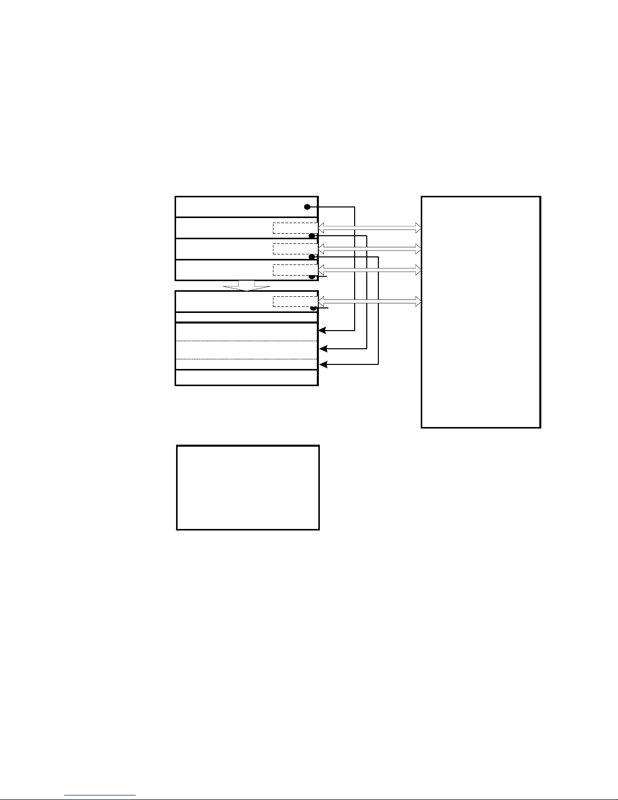
RAM area inside of the card. Figure 4 shows the mapping of the CIA and optional CSA space for an SDIO
card.
6.2 Register Access Time
All registers in SDIO only cards and the SDIO portion of Combo cards must complete read and write data
transfer in less than 1 second. The host can use 1 second as the timeout value for a non-responding location.
If a functions needs to support an access time greater than 1 second, the card maker will use some function
specific method that is not defined in this specification. The 1-second response time is dependant on the
SDCLK frequency. If the Average frequency of the SDCLK is less than 100KHz then the card may not be able
to respond within the 1-second limit. The host should adjust the timeout in the case the average frequency of
the SDCLK is less than 100KHz.
6.3 Interrupts
All SDIO hosts shall support interrupts in both the SPI and 1-bit SD modes. Each function within an SDIO or
Combo card may implement interrupts as needed. The interrupt used on SDIO functions is a type commonly
called “level sensitive”. Level sensitive means that any function may signal for an interrupt at any time, but
once the function has signaled an interrupt, it will not release (stop signaling) the interrupt until the cause of the
interrupt is removed or commanded to do so by the host. Since there is only 1 interrupt line, it may be shared
by multiple interrupt sources. The function shall continue to signal the interrupt until the host responds and
clears the interrupt. Since multiple interrupts may be active at once, it is the responsibility of the host to
determine the interrupt source(s) and deal with it as needed. This is done on the SDIO function by the use of
two bits, the interrupt enable and interrupt pending. Each function that may generate an interrupt has an
interrupt enable bit. In addition, the SDIO card has a master interrupt enable that controls all functions. An
interrupt will only be signaled to the SD bus if both the function’s enable and the card’s master enable are set.
The second interrupt bit is called interrupt pending. This read-only bit tells the host which function(s) may be
signaling for an interrupt. There is an interrupt pending bit for each function that can generate interrupts. These
bits are located in the CCCR area.
17
) registers possible for each I/O
10
Page 15

SDIO Simple Specification Version 1.0 DO NOT COPY ©Copyright SD Association, 2000, 2001
6.4 Suspend/Resume
Within a multi-function SDIO or a Combo card, there are multiple devices (I/O and memory) that must share
access to the SD bus. In order to allow the sharing of access to the host among multiple devices, SDIO and
combo cards can implement the optional concept of suspend/resume. If a card supports suspend/resume, the
host may temporarily halt a data transfer operation to one function or memory (suspend) in order to free the
bus for a higher priority transfer to a different function or memory. Once this higher-priority transfer is complete,
the original transfer is re-started where it left off (resume). Support of suspend/resume is optional on a
per-card basis. If suspend/resume is implemented, it shall be supported by the memory (if any) of a Combo
card and all I/O functions except 0 (the CIA). Note that the host can suspend multiple transactions and resume
them in any order desired. I/O function 0 does not support suspend/resume. Note that Suspend/Resume is
defined only for the SD 1 and 4-bit modes. It does not apply to SPI transfers.
6.5 Read Wait (Optional)
Host devices built to the SD Physical specification version 1.01 must control the SDCLK to stop the read data
block output from a card executing a multiple read command whenever the host cannot accept more data.
During the time that the host has stopped the SDCLK, a CMD52 cannot be issued. This limitation causes a
problem in that a host device built to the SD Physical specification version 1.01 cannot perform the I/O
command during a multiple read cycle.
In order to eliminate this limitation, the SDIO specification adds the read wait control to enable the host to issue
CMD52 during a multiple read cycle. Read Wait uses the DAT[2] line to allow the host to signal the card to
temporarily halt the sending of read data by a card. This feature is optional for an SDIO or combo card.
However, if an SDIO or combo supports Read Wait, all functions and any memory must support read wait.
Note that Read Wait is defined only for the SD 1 and 4-bit modes. It does not apply to SPI transfers.
To determine if a card supports the Read Wait protocol, the host must test SRW capability bit in the Card
Capability byte of the CCCR. If a card does not support the Read Wait protocol, the only means a host has to
stall (not abort) data in a read multiple command is to control the SDCLK.
11
Page 16
SDIO Simple Specification Version 1.0 DO NOT COPY ©Copyright SD Association, 2000, 2001
6.6 SDIO Fixed Internal Map
The SDIO card has a fixed internal register space and a Function unique area. The fixed area contains
information about the card and certain mandatory and optional registers in fixed locations. The fixed locations
allow any host to obtain information about the card and perform simple operations such as enable in a
common manner. The function unique area is a per-function area, which is defined by the vendor and different
for each SDIO function. Figure 4 shows the internal map of an SDIO card with multiple functions.
CIA (Function 0)
0x000000-0x0000FF
0x000200-0x0002FF
0x000300-0x0003FF
0x000700-0x0007FF
0x000800-0x000FFF
0x001000-0x017FFF
0x018000-0x01FFFF
0x000000-0x01FFFF
CCCR
FBR (Function 1)0x000100-0x0001FF
FBR (Function 2)
FBR (Function 3)
FBR (Function 7)
RFU
CIS Area
(common and per-function)
RFU
Window
Window
Window
Window
128K Register Space
(function 1-7)
Function Unique
X
X
CIS Pointers
16 MB optional
Code Storage
Area
(CSA)
6.7 Common I/O Area (CIA)
The Common I/O Area (CIA) shall be implemented on all SDIO cards. The CIA is accessed by the host via I/O
reads and writes to function 0. The registers within the CIA are provided to enable/disable the operation of the
I/O function(s), control the generation of interrupts and optionally load software to support the I/O functions.
The registers in the CIA also provide information about the function(s) abilities and requirements. There are
three distinct register structures supported within the CIA. They are:
1. Card Common Control Registers (CCCR)
2. Function Basic Registers (FBR)
3. Card Information Structure (CIS)
12
Figure 4 SDIO Internal Map
Page 17

SDIO Simple Specification Version 1.0 DO NOT COPY ©Copyright SD Association, 2000, 2001
6.8 Card Common Control Registers (CCCR)
The Card Common Control Registers allow for quick host checking and control of an I/O card’s enable and
interrupts on a per card (master) and per function basis. The bits in the CCCR are mixed Read/Write and read
only. If any of the possible 7 functions are not provided on an SDIO card, the bits corresponding to unused
functions shall all be read-only and read as 0. All reserved for future use bits (RFU) shall be read-only and
return a value of 0. All writeable bits are set to 0 after power-up or reset. Access to the CCCR is possible even
after initialization when the I/O functions are disabled. This allows the host to enable functions after
initialization.
6.9 Function Basic Registers (FBR)
In addition to the CCCR, each supported I/O function has a 256-byte area used to allow the host to quickly
determine the abilities and requirements of each function and to enable software loading. The address of this
area is from 0x00n00 to 0x00nFF where n is the function number (0x1 to 0x7).
6.10 Card Information Structure (CIS)
The Card Information Structure provides more complete information about the card and the individual
functions. The CIS is the common area to read information about all I/O functions that exist in a card. The
design is based on the PC Card16 design standardized by PCMCIA. All cards that support I/O must have a
common CIS and a CIS for each function. The CIS is accessed by reads to a fixed area. This one area serves
the card as a Common CIS and also as the storage area for each function. The common area and each
function have a pointer to the start of its CIS within this memory space.
6.11 Multiple Function SD Cards
Multiple Function SDIO Cards shall have a separate set of Configuration registers for each function on the
card. Multiple Function SDIO Cards shall use a combination of a CIS common to all functions on the card and
a separate function-specific CIS specific to each function on the card. The common CIS describes features
that are common to all functions on the card. Each function-specific CIS describes features specific to a
particular function on the SDIO Card.
6.12 Embedded I/O Code Storage Area (CSA)
In order to support the concept of “Plug-and-Play” for SDIO cards, each function contained in a card may need
to contain a block of memory for the storage of drivers and/or applications. In addition, since the same SDIO
card may be used on multiple different host platforms, several different versions of the code may be needed for
each function. One option is to store these programs in a standard SD Memory section of a combo card.
Alternately, a standard access means to load the code is contained in the optional Code Storage Area (CSA).
The CSA is a separate 16MB memory area that is accessed using the CSA address pointer and the CSA
window register contained in the FBR registers. Note that each function may have it’s own CSA to support it.
The CSA data can be read only or R/W. The actual storage method for the CSA is not a part of this
specification and left to the implementers.
13
Page 18

SDIO Simple Specification Version 1.0 DO NOT COPY ©Copyright SD Association, 2000, 2001
7. SDIO Interrupts
In order to allow the SDIO card to interrupt the host, an interrupt function is added to a pin on the SD interface.
Pin number 8, which is used as DAT[1] when operating in the 4-bit SD mode, is used to signal the card’s
interrupt to the host. The use of interrupt is optional for each card or function within a card. The SDIO interrupt
is “level sensitive”, that is, the interrupt line must be held active (low) until it is either recognized and acted
upon by the host or de-asserted due to the end of the Interrupt Period (see 7.1.2). Once the host has serviced
the interrupt, it is cleared via some function unique I/O operation. All hosts must provide pull-up resistors on all
data lines DAT[3:0] as described in section 6 of the SD Physical Specification.
7.1 Interrupt Timing
The operation of the interrupt pin is different between the SPI mode and the SD mode. The operation of the
interrupt pin is defined as follows:
7.1.1 SPI and SD 1-bit mode interrupts
In the SPI and 1-bit SD mode, Pin 8 is dedicated to the interrupt function. Thus, in the SPI and SD 1-bit modes
there are no timing constraints on interrupts. A card in the SPI or 1-bit SD mode signals an interrupt to the host
by asserting pin 8 low. The host detects this pending interrupt using a level sensitive input. The host is
responsible for clearing the interrupt.
Important Note: The 1.0 version of this specification does not indicate if a card can assert the interrupt line when
that card is not selected (CS=1). The consensus of the SDIO Working Group is that a card in the SPI mode may not
assert the IRQ signal if the card is not selected. This point will be clarified in future revisions of this specification.
Until that time, host and card developers should not assert or expect the IRQ signal unless that card is selected. Also,
in future revisions of this specification, the ability of a SDIO card in the SPI mode to generate interrupts while not
selected will be added.
7.1.2 SD 4-bit mode
Since Pin 8 is shared between the IRQ and DAT[1] use in the 4-bit SD mode, an interrupt shall only be sent by
the card and recognized by the host during a specific time. The time that a low on Pin 8 will be recognized as
an interrupt is defined as the Interrupt Period.
An SDIO host shall only sample the level on Pin 8 (DAT[1]/IRQ) into the interrupt detector during the Interrupt
Period. At all other times, the host interrupt controller shall ignore the level on Pin 8. Note that the Interrupt
Period is applicable for both memory and I/O operations The definition of the Interrupt Period is different for
operations with single block and multiple block data transfer.
This Interrupt Period is intended to prevent the interaction between the DAT[1] data and the interrupt signals
on a common pin. Note that the Interrupt period includes the times when there is no command or data activity
between the host and the card. In the case where the interrupt mechanism is used to wake the host while the
card is in a low power state (i.e. no clocks), Both the card and the host shall be placed into the 1-bit SD mode
prior to stopping the clock.
7.1.3 Interrupt Clear Timing
Since the SDIO card uses level sensitive interrupts, the host must clear pending interrupts with an I/O read or
write to some function unique area. In some host implementations, the sending of a CMD52 to the card is
handled by host adapter hardware while the host CPU can execute other operations. This condition may allow
an interrupt that has already been handled to re-interrupt the host if the timing of the interrupt clear is not
controlled. To prevent this condition, Any SDIO card that implements interrupts must follow some required
timing with respect to removing the interrupt from the DAT[1] line after the write to the function unique area that
clears the interrupt. The clearing of the interrupt can be caused by an IO write in a function unique method, or
by a function unique IO read.
14
Page 19
SDIO Simple Specification Version 1.0 DO NOT COPY ©Copyright SD Association, 2000, 2001
8. SDIO Physical Properties
8.1 SDIO Size
The SDIO card is compatible with host sockets designed for SD memory cards. In addition, the SDIO cards
can be extended to allow for external connectors, antennas etc. With the exception of the write protect switch,
all SDIO cards must meet the mechanical specifications described in the SD Physical spec version 1.01 for
that portion of the card that is not extended. The WP switch is not supported by hosts for SDIO only cards (see
9.3 for additional information).
8.2 SDIO Card Package
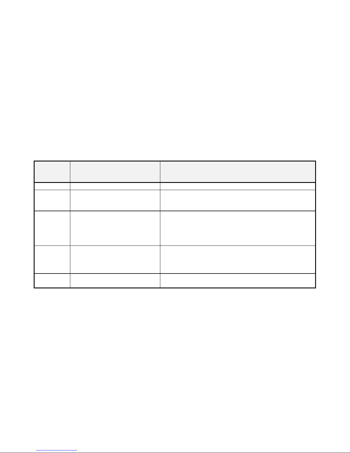
An SDIO card shall meet all requirements for Card Packaging identified in section 8.1 of the SD Physical
Specification version 1.01 except as noted in Table 3.
SD
Physical
section
8.1.1 External signal contacts (ESC) NONE
8.1.2 Design and format
8.1.3 Reliability and durability Bending and Torque shall be measured at a point 32mm
8.1.4 Electrical Static Discharge
(ESD) Requirements
8.1.5 Quality assurance Not applicable, SDIO card support of unique ID is
Title Exceptions for SDIO
32mm size limit does not apply to SDIO. In addition, any
dimension limits do not apply in the SDIO extended area.
See 8.1 and 9.2
away from contact end irrespective of actual length. WP
requirements apply only if WP switch installed (not
supported on SDIO only cards). Drop test does not apply
to SDIO cards.
Contact Pads test shall apply only to the 9 SD pins, not
any additional vendor specific contacts. Non Contact
Pads area for ESD discharge testing shall be in the
24mm by 32mm area of a standard SD card
optional
Table 3 SDIO exceptions to SD physical section 8.1 requirements
15
Page 20

SDIO Simple Specification Version 1.0 DO NOT COPY ©Copyright SD Association, 2000, 2001
9. SDIO Mechanical Extensions
In order to implement some function in the SD card form factor, some extensions to the standard card size and
constructions may be needed. There are two areas of extension defined for SDIO devices. Both of these
extensions are optional, and may be used by card vendors based upon their needs. The two extensions are:
1. Additional ESD/EMI ground contact
2. Extended case dimensions
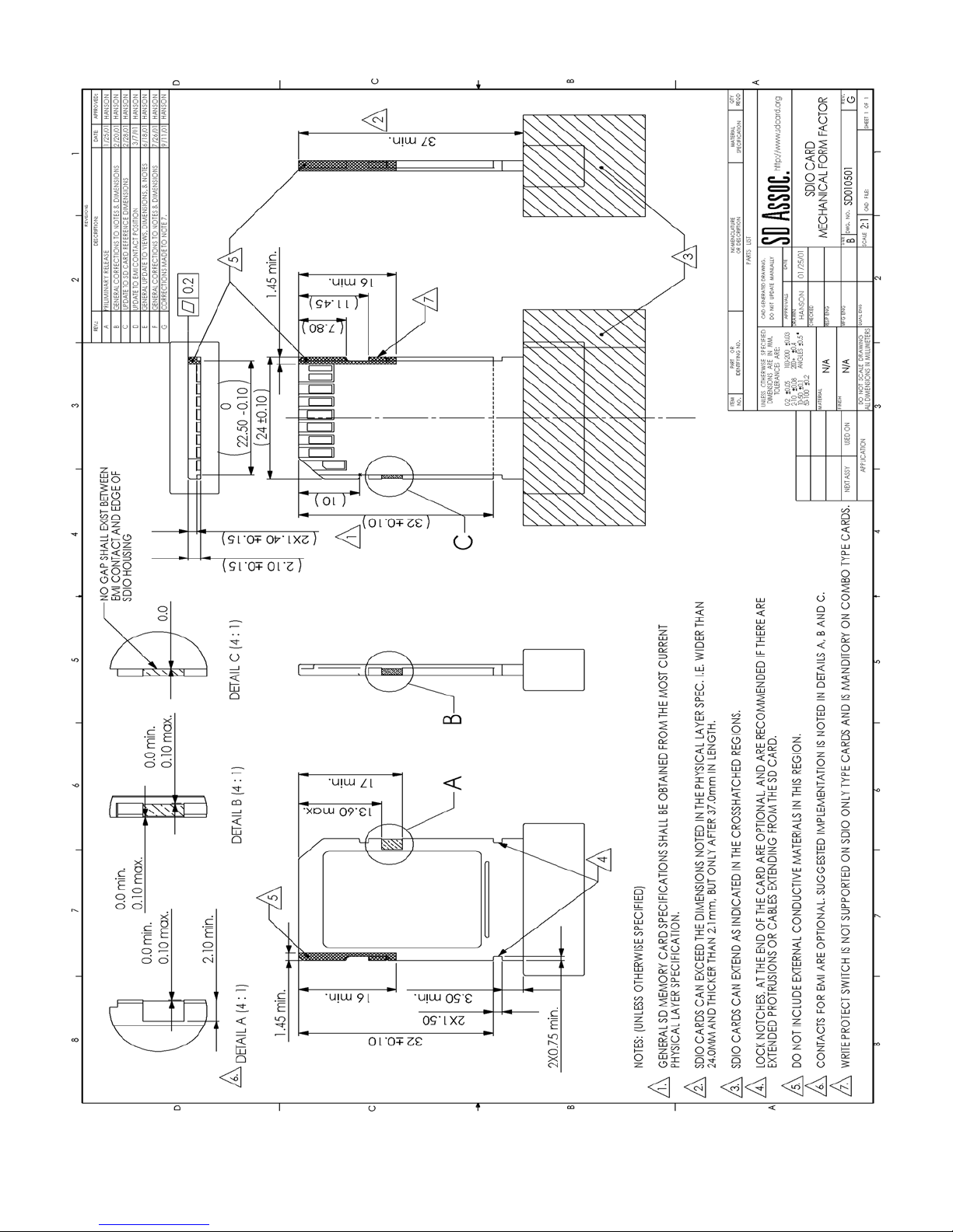
Figure 5 shows the details of both optional extensions.
9.1 Additional ESD/EMI Ground Point
For some SDIO devices, there may be a need for a lower impedance ground connection to the host. This may
be needed to reduce the card’s EMI emission or susceptibility. Also, an additional ground may be needed to
discharge ESD on insertion or operation. If additional grounding is required, the card may implement an
additional ground contact as shown in Figure 5.
9.2 Extended Case
In order to provide useful I/O devices in the SDIO form factor, it may be necessary to extend the size of the
case to provide room for connectors, antennas etc. In order to provide the extension room and maintain
compatibility with existing SD hosts, the SDIO extension area has been defined. Figure 5 shows this extension
area. The SDIO card vendor may extend the case of its SDIO products within the area identified. Please note
that there is no limit in this specification as to the amount or direction of growth in this area. The vendor is
cautioned that extensions may cause interference problems with SD hosts, depending on the amount and
direction of growth. The drawing shows 2 additional lock notches beyond the normal SD area. These notches
are intended to provide additional retention for SDIO devices to prevent accidental withdrawal due to cables or
additional weight of extended cases. The support of these notches is optional for both the host and the card
vendor, but their use is highly recommended for both cards and hosts to prevent unintended disconnects.
9.3 Write Protect Switch
The WP switch is not supported by hosts for SDIO only cards. Because the host does not support the Write
Protect function for SDIO only cards, it is suggested that these cards be built without cutouts or notches in the
case at the write protect location. If the maker of an SDIO card chooses to add the Write Protect cutout, it shall
be made to signal a write-enabled device (see Figure 5). If the SDIO card is a combo card, the WP switch is
mandatory. For this case, it must meet all specifications from the SD Physical Specification.
16
Page 21
SDIO Simple Specification Version 1.0 DO NOT COPY ©Copyright SD Association, 2000, 2001
Figure 5 SDIO Mechanical Extensions
17
Page 22

SDIO Simple Specification Version 1.0 DO NOT COPY ©Copyright SD Association, 2000, 2001
10. SDIO Power
10.1 SDIO Card Initialization Voltage
SDIO cards follow the same voltage and current requirements as SD memory cards. This means that an SDIO
or combo card must allow basic communication with the card at an initial voltage range of 2.0 to 3.6V. This
basic communication is defined as: CMD5 with arg=0, CMD0, CMD15 and CMD58.
10.2 SDIO Power Consumption
The SDIO cards are intended to operate in mobile devices that have limited power sources available. Because
the host device’s battery life may be significantly reduced if the SDIO device draws excessive power, a primary
goal of SDIO designers should be low power. By reducing power consumption to a minimum, Host battery life
and consumer satisfaction will be enhanced. The following power data represents the maximum that a SDIO
device may draw. It is important for designers to note that a low power host may reject any SDIO card that
identifies itself as drawing more power that the host is willing to supply, thus lower power devices may have a
competitive advantage in the market.
10.3 SDIO Current
Upon initial insertion, SDIO and combo cards shall draw a maximum of 15mA, averaged over a 1 second
interval. Note that a memory or combo card built to meet the SD Physical specification version 1.0 may not
meet this initial current requirement. Any card built to meet a specification later than 1.01 shall meet this
requirement.
Once the card receives the CMD5 or ACMD41 initialization commands, the average current shall be:
• 50 mA or less, averaged over a 400 µS period for SDIO only cards
• 100 mA or less, averaged over a 1 second period for combo cards
This current limit will continue until the card exits the initialization procedure (Disabled for SD and in_idle_state
for SPI).
18
Page 23

SDIO Simple Specification Version 1.0 DO NOT COPY ©Copyright SD Association, 2000, 2001
11. Abbreviations and Terms
Block A number of bytes, basic data transfer unit
CCCR Common Card Control Registers
CD Connect/Disconnect
CIA Common Information Area
CID Card IDentification number register
CIS Card Information Structure
CLK Clock signal
CMD Command line or SD bus command (if extended CMDXX)
Combo Card A card that includes both SDIO and SD memory
CRC Cyclic Redundancy Check
CS Chip or Card Select
CSA Code Storage Area
CSD Card Specific Data register
DAT[x] Data line where x is in the range of 0 to 3
DSR Driver Stage Register
ECC Error Correction Code
EMI Electro-Magnetic Interference
ESC External Signal Contacts
ESD Electro-Static Discharge
FAT File Allocation Table
FBR Function Basic Registers
FIFO First In-First Out buffer
Flash a type of multiple time programmable non volatile memory
Function An IO device contained within an SDIO card
hi-Z A three-state driver in the high-impedance state
Interrupt A signal from the SDIO device to the host signaling the need for
attention
Interrupt Period The times that a card may generate an interrupt signal on the SD bus
Legacy Slot SD Slot that supports only the SD 1.01 specification
LOW, HIGH binary interface states with defined assignment to a voltage level
MBIO Multi-Block IO
MMC MultiMedia Card
MSB, LSB the Most Significant Bit or Least Significant Bit
OCR Operation Conditions Register
PCMCIA Personal Computer Memory Card International Association
PnP Plug and Play a means to identify an SDIO device and optionally load
applications and/or drivers without user intervention
R/O Read Only
R/W Read or Write
19
Page 24

SDIO Simple Specification Version 1.0 DO NOT COPY ©Copyright SD Association, 2000, 2001
RAW Read After Write
RCA Relative Card Address register
Resume Re-starting the temporarily halted data transfer
RFU Reserved for Future Use. Normally Read-Only and set to 0
ROM Read Only Memory
RWC Read Wait Control
SCR SD Configuration Register
SD Secure Digital
SDA SD Association
SDCLK SD clock signal
SDIO Secure Digital I/O
SDIO aware A host designed to support the signals and protocol of SDIO devices
SPI Serial Peripheral Interface
Stuff bit(s) Filling bit(s) to ensure fixed length frames for commands and
responses.
Suspend Temporarily halting the transfer of data
TBD To Be Determined (in the future)
Three-state
driver
A driver stage which has three output driver states: HIGH, LOW and
high impedance (which means that the interface does not have any
influence on the interface level)
Tuple Data blocks in a linked list or chain format
VDD + Power supply
VSS Power supply ground
W/O Write Only
WP Write Protect
20
Page 25
SDIO Simple Specification Version 1.0 DO NOT COPY ©Copyright SD Association, 2000,2001
Appendix A
(Normative)
A.1 SD and SPI Command List
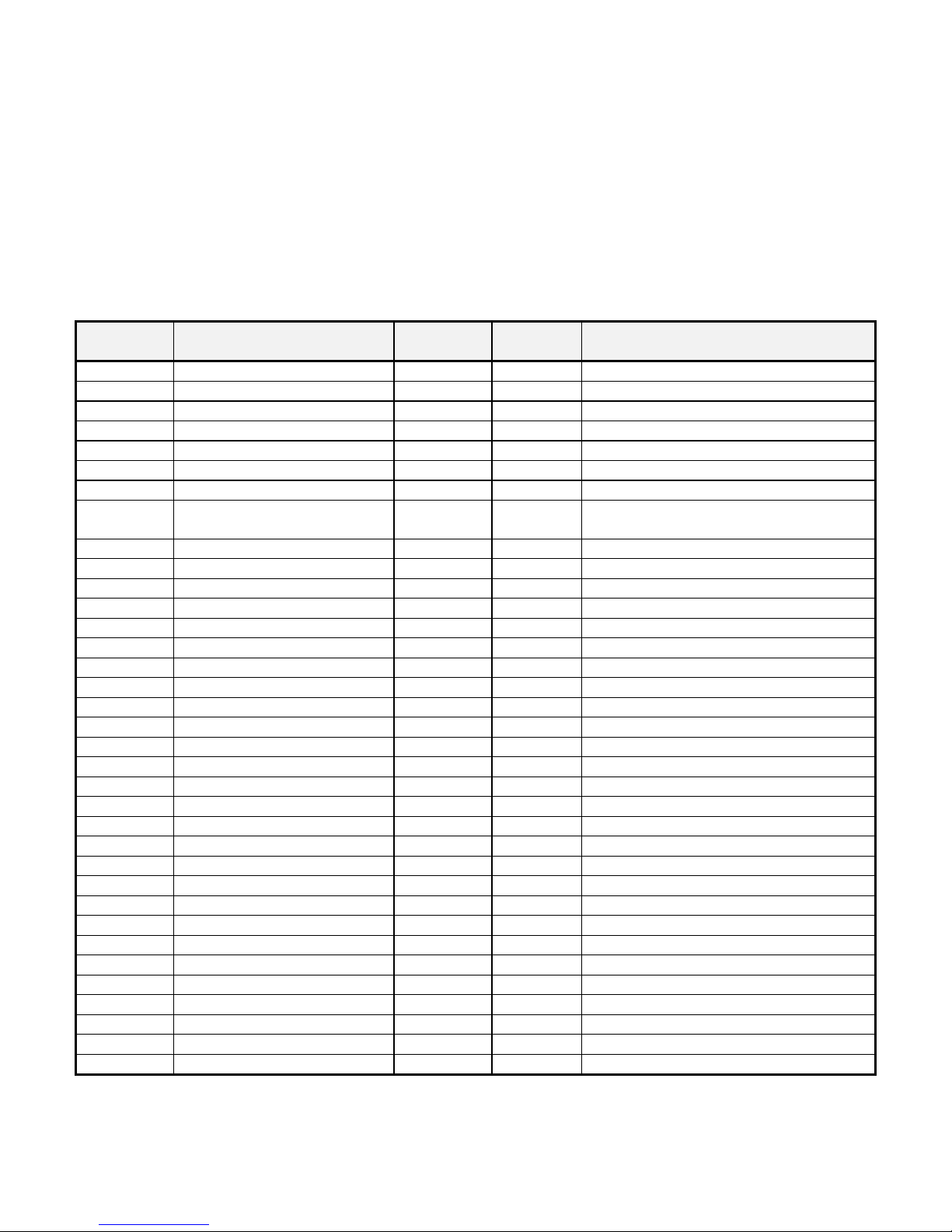
Table 4 and Table 5 show the commands that are supported by SD memory and SDIO devices in both SPI and
SD modes. If a command is not identified as either mandatory or optional, then it is not supported by that
device.
Supported
Commands
CMD0 GO_IDLE_STATE Mandatory Mandatory Used to change from SD to SPI mode
CMD2 ALL_SEND_CID Mandatory CID not supported by SDIO
CMD3 SEND_RELATIVE_ADDR Mandatory Mandatory
CMD4 SET_DSR Optional DSR not supported by SDIO
CMD5 IO_SEND_OP_COND Mandatory
CMD7 SELECT/DESELECT_CARD Mandatory Mandatory
CMD9 SEND_CSD Mandatory CSD not supported by SDIO
CMD10 SEND_CID Mandatory CID not supported by SDIO
CMD12 STOP_TRANSMISSION Mandatory
CMD13 SEND_STATUS Mandatory Card Status includes only SDMEM information
CMD15 GO_INACTIVE_STATE Mandatory Mandatory
CMD16 SET_BLOCKLEN Mandatory
CMD17 READ_SINGLE_BLOCK Mandatory
CMD18 READ_MULTIPLE_BLOCK Mandatory
CMD24 WRITE_BLOCK Mandatory
CMD25 WRITE_MULTIPLE_BLOCK Mandatory
CMD27 PROGRAM_CSD Mandatory CSD not supported by SDIO
CMD28 SET_WRITE_PROT Optional
CMD29 CLR_WRITE_PROT Optional
CMD30 SEND_WRITE_PROT Optional
CMD32 ERASE_WR_BLK_START Mandatory
CMD33 ERASE_WR_BLK_END Mandatory
CMD38 ERASE Mandatory
CMD42 LOCK_UNLOCK Optional
CMD52 IO_RW_DIRECT Mandatory
CMD53 IO_RW_EXTENDED Mandatory Block mode is optional
CMD55 APP_CMD Mandatory
CMD56 GEN_CMD Mandatory
ACMD6 SET_BUS_WIDTH Mandatory
ACMD13 SD_STATUS Mandatory
ACMD22 SEND_NUM_WR_BLOCKS Mandatory
ACMD23 SET_WR_BLK_ERASE_COUNT Mandatory
ACMD41 SD_APP_OP_COND Mandatory
ACMD42 SET_CLR_CARD_DETECT Mandatory
ACMD51 SEND_SCR Mandatory SCR not supported by SDIO
Abbreviation
SDMEM
System
SDIO
System
Comments
Table 4 SD Mode Command List
A
Page 26
SDIO Simple Specification Version 1.0 DO NOT COPY ©Copyright SD Association, 2000,2001
Supported
Commands
CMD0 GO_IDLE_STATE Mandatory Mandatory Used to change from SD to SPI mode
CMD1 SEND_OP_COND Mandatory
CMD5 IO_SEND_OP_COND Mandatory
CMD9 SEND_CSD Mandatory CSD not supported by SDIO
CMD10 SEND_CID Mandatory CID not supported by SDIO
CMD12 STOP_TRANSMISSION Mandatory
CMD13 SEND_STATUS Mandatory Card Status includes only SDMEM information.
CMD16 SET_BLOCKLEN Mandatory
CMD17 READ_SINGLE_BLOCK Mandatory .
CMD18 READ_MULTIPLE_BLOCK Mandatory
CMD24 WRITE_BLOCK Mandatory
CMD25 WRITE_MULTIPLE_BLOCK Mandatory
CMD27 PROGRAM_CSD Mandatory CSD not supported by SDIO.
CMD28 SET_WRITE_PROT Optional
CMD29 CLR_WRITE_PROT Optional
CMD30 SEND_WRITE_PROT Optional
CMD32 ERASE_WR_BLK_START Mandatory
CMD33 ERASE_WR_BLK_END Mandatory
CMD38 ERASE Mandatory
CMD42 LOCK_UNLOCK Optional
CMD52 IO_RW_DIRECT Mandatory
CMD53 IO_RW_EXTENDED Mandatory Block mode is optional
CMD55 APP_CMD Mandatory
CMD56 GEN_CMD Mandatory
CMD58 READ_OCR Mandatory
CMD59 CRC_ON_OFF Mandatory Mandatory
ACMD13 SD_STATUS Mandatory
ACMD22 SEND_NUM_WR_BLOCKS Mandatory
ACMD23 SET_WR_BLK_ERASE_COUNT Mandatory
ACMD41 SD_APP_OP_COND Mandatory
ACMD42 SET_CLR_CARD_DETECT Mandatory
ACMD51 SEND_SCR Mandatory SCR includes only SD-MEM information.
Abbreviation
SDMEM
System
SDIO
System
Comments
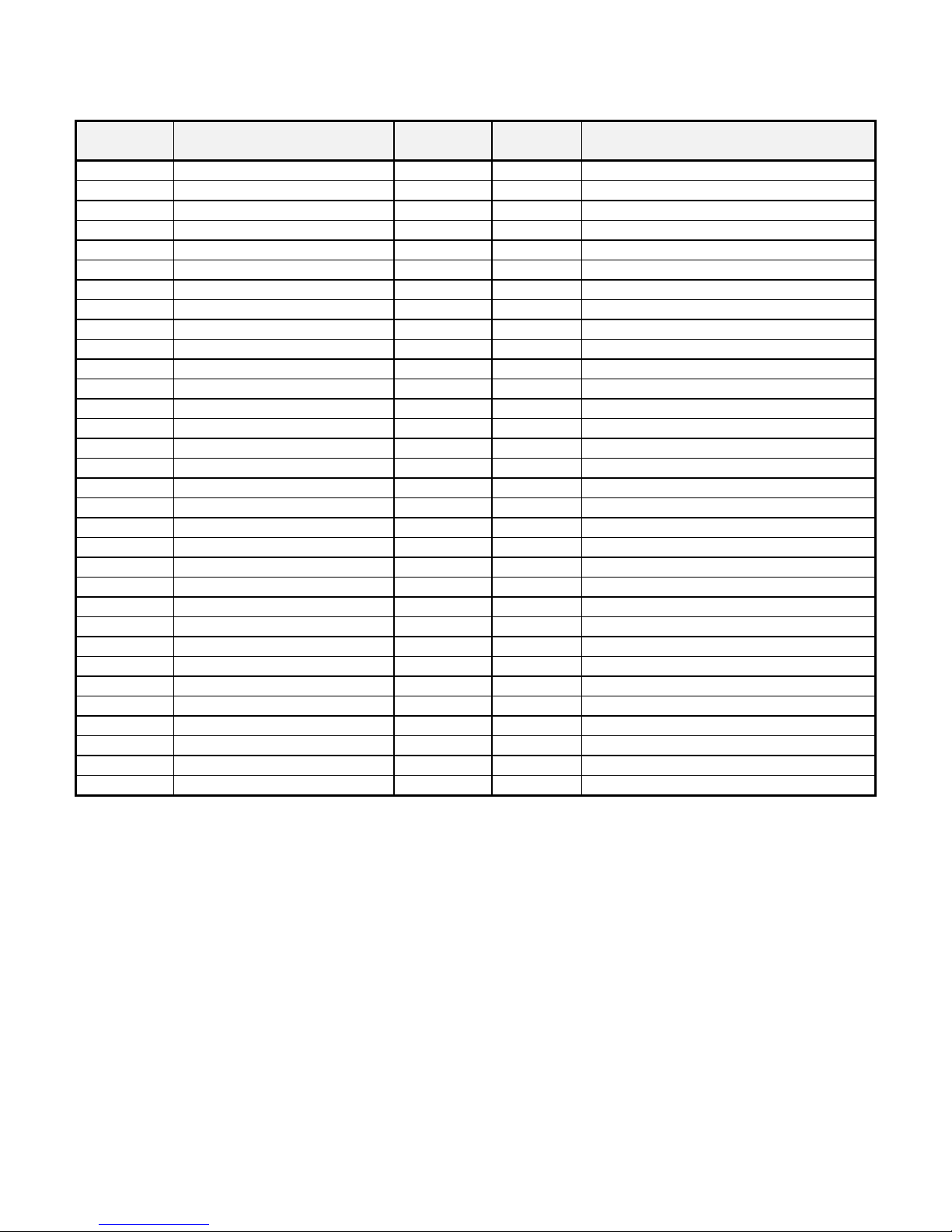
Table 5 SPI Mode Command List
B
Page 27

SDIO Simple Specification Version 1.0 DO NOT COPY ©Copyright SD Association, 2000,2001
Appendix B
(Normative)
B.1 Normative References
The following documents are referenced by this specification. The reader is directed to the respective owners
to obtain copies.
1) SD Memory Card Specifications
Part 1 PHYSICAL LAYER SPECIFICATION
Version 1.01 September 2000
2) SD Memory Card Specifications
Part 2 FILE SYSTEM SPECIFICATION
Version 1.0 February 2000
3) ISO/IEC9293:1994
Information technology - Volume and file structure of disk cartridges for information interchange
4) PC CARD STANDARD Release 8 2001
Volume 4 Metaformat Specification
5) The MultiMedia Card System Specification
MMCA Technical Committee Version 2.2
C
Page 28
SDIO Simple Specification Version 1.0 DO NOT COPY ©Copyright SD Association, 2000,2001
Appendix C
(Informative)
C.1 Example SDIO Controller Design
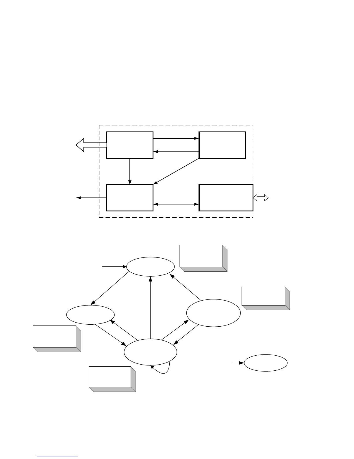
Figure 6 shows an example of an SDIO controller design. In this example, two independent state machines are
used. The first is the Bus State machine, which communicates with the host and maintains bus states. Figure
7 shows an example state table for this machine. The second machine is used to communicate and control the
function(s) in the card. This machine maintains control of function states such as Exec, Ready and interrupts.
An example state table for this machine can be seen in Figure 8.
Response
I/O current state
CCCR Read Data
Commands
accepted in “STB”
CMD3, CMD7,
CMD15
CMD52
CMD53
Power On
Standby
State
CMD7 with
correct RCA
accepted in “CMD”
CMD7, CMD52,
CMD53, CMD15
Bus State
Machine
Bus Status (BS),
Function Select
CCCR Registers
Handshake
Signals
SDIO Card
Interrupt Status,
Interrupt Control
Function State
Machine
IORD Y ,
Exec Flag,
Ready Flag
Function
Figure 6 SDIO Internal State Machine example
Commands
accepted in “INI”
CMD5, CMD3
CMD15
CMD52 Reset
(Dat Bus Active)
Execution complete
Function Suspend
CMD52 Abort
RCA
function
Transfer
State
BS=1
CMD15 or OCR
mismatch
CMD53 to invalid function can be:
y
y
y
CMD3
Commands
Initialization
CMD52 Reset
CMD7 with
incorrect RCA
Command
(Dat Bus Free)
State
CMD53 (to valid
function)
Function
Resume
State
BS=0
CMD7 with correct
CMD53 to invalid
Commands
accepted in “TRN”
CMD52
Inactive
State
I/O Disable or I/O Not Ready (IORDY=0)
I/O Function number error in response
I/O Function already Suspended
Figure 7 State Diagram for Bus State Machine
D
Page 29
SDIO Simple Specification Version 1.0 DO NOT COPY ©Copyright SD Association, 2000,2001
Read Complete
Abort asserted
Continue Read
Multiple
Power on,
IO Reset from
any state
CMD53 Read
Read Not Ready
IOEN=1
IORDY=1
RF=0
EX=1
Transfer Ready
Set IOEN=0
Go Inactive request
Abort asserted
Read Data
Disable State
IOEN=0
IORDY=0
RF=0
EX=0
Set IOEN=1
IO ready
IO Ready State
IOEN=1
IORDY=1
RF=0
EX=0
CMD53 Write
Write Data Transfer State
Write Busy
Set IOEN=1
IO not ready
IO ready
Write Complete (no busy)
IOEN=1
IORDY=1
RF=1
EX=1
Set IOEN=0,
Go Inactive request
IO not ready
Abort asserted
Continue Write
Multiple
I
O NOT Ready State
IOEN=1
IORDY=0
RF=0
EX=0
Write Complete
Abort asserted
and block write
,
IO Fuction
invalid/Fail
(No busy)
complete
Read Data Transfer
State
IOEN=1
IORDY=1
RF=1
EX=1
Write Busy
IOEN=1
IORDY=1
RF=0
EX=1
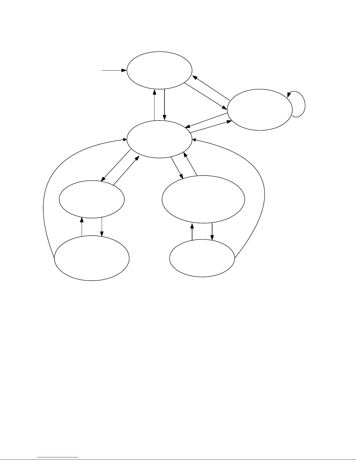
Figure 8 State Diagram for Function State Machine
E
 Loading...