


Bartles Industrial Estate Tel: +44 (0)1209 314 608 scitec@scitec.uk.com
North Street, Redruth Fax: +44 (0)1209 314 609 www.scitec.uk.com
Cornwall TR15 1HR Fax2: +44 (0)870 1600 860
MODEL 441 ANALOG OEM
DUAL PHASE LOCK-IN AMPLIFIER
&
MODEL 430 ANALOG OEM
SINGLE PHASE LOCK-IN AMPLIFIER
USER MANUAL V1.2
Boston Electronics Corporation, 91 Boylston Street, Brookline MA 02445
(800)347-5445 or (617)566-3821 * fax (617)731-0935 * boselec@boselec.com * www.boselec.com

Bartles Industrial Estate Tel: +44 (0)1209 314 608 scitec@scitec.uk.com
North Street, Redruth Fax: +44 (0)1209 314 609 www.scitec.uk.com
Cornwall TR15 1HR Fax2: +44 (0)870 1600 860
CONTENTS
1 POWER SUPPLY
1.1 Power Connections
1.2 Earth Connections for High Voltage / E S D Protect ion
2 BOARD LAYOUT
3 OPERATION
3.1 Block Diagrams
3.2 Lock-in Amplifier Theory
4 INPUT STAGE
4.1 Jumper Settings Overview
4.2 Single Ended DC Coupled Input
4.3 Single Ended AC Coupled Input
4.4 Single Ended Current Input
4.5 Differential Input
4.6 Low Impedance Differential Input
5 FIRST STAGE AMPLIFICATION
6 LOW PASS FILTER TIME CONSTANT SETTINGS
6.1 First Time Constant Settings
6.2 Second Time Constant Settings
7 OUTPUT STAGE
7.1 Output Stage Amplification
7.2 Fine Gain Adjust
7.3 Offset Adjust
7.4 R Calculation
7.5 R Calculati on Time Constant
8 REFERENCE SECTION
8.1 Fine Phase Control
8.2 Coarse Phase Control and 1F/2F Operation
9 OVERALL SYSTEM GAIN AND DYNAMIC RESERVE
9.1 Dynamic Reserve
9.2 Maximum Signal Size Up To The Low Pass Filter
9.3 Maximum Signal Size From Low Pass Filter to Output
9.4 Example Gain Settings
Boston Electronics Corporation, 91 Boylston Street, Brookline MA 02445
(800)347-5445 or (617)566-3821 * fax (617)731-0935 * boselec@boselec.com * www.boselec.com
Bartles Industrial Estate Tel: +44 (0)1209 314 608 scitec@scitec.uk.com
North Street, Redruth Fax: +44 (0)1209 314 609 www.scitec.uk.com
Cornwall TR15 1HR Fax2: +44 (0)870 1600 860
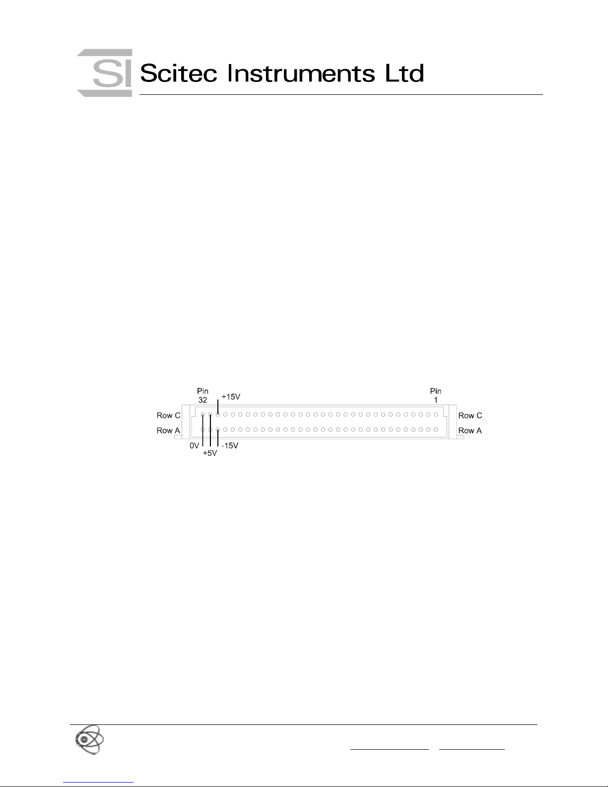
1 POWER SUPPLY
1.1 Power Connections
A well regulated ±15V & +5V supply is required to power the lock-in amplifier board. 50mA
per supply is required for the 441 and 35mA per supply are required for the 430. Power is
supplied via a 64 pin type C DIN41612 connector as follows:
0V Pin 32A & Pin 32C
+5V Pin 31A & Pin 31C
+15V Pin 30C
-15V Pin 30A
No other pins on the DIN41612 connector are used.
Please note that the pin numbers are labelled on the back of the connector next to the solder
pins and as per Figure 1. Please also note that some connectors have P1~A on the front face.
Rather confusingly, this A is actually next to row C pins.
Figure 1 Power Connections
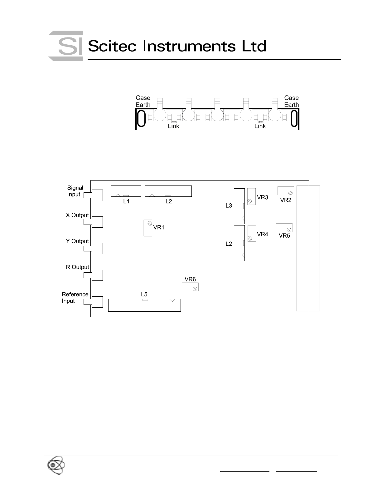
1.2 Earth Connections for High Voltage / ESD Protection
As lock-in amplifiers are often used in optics applications with lasers driven by high voltage
power supplies, it is sometimes important to protect equipment from high voltage discharges.
Electro-Static Discharge (ESD) protection is also important and is a requirement for CE
marking. All inputs and outputs to the 430 and 441 are protected by transient suppression
devices but for full protection a case earth connection is required directly to the PCB.
To give full protection to the board from high voltages, a thick earth wire should be bonded to
the board at one or other or both of the points shown in Figure 2 and connected to case or
chassis ground by as short a lead as possible. The two links also indicated should be added to
the board. Please note that these earth connections are not connected to signal ground on the
PCB.
Boston Electronics Corporation, 91 Boylston Street, Brookline MA 02445
(800)347-5445 or (617)566-3821 * fax (617)731-0935 * boselec@boselec.com * www.boselec.com
Bartles Industrial Estate Tel: +44 (0)1209 314 608 scitec@scitec.uk.com
North Street, Redruth Fax: +44 (0)1209 314 609 www.scitec.uk.com
Cornwall TR15 1HR Fax2: +44 (0)870 1600 860
Figure 2 Case Earth Connections
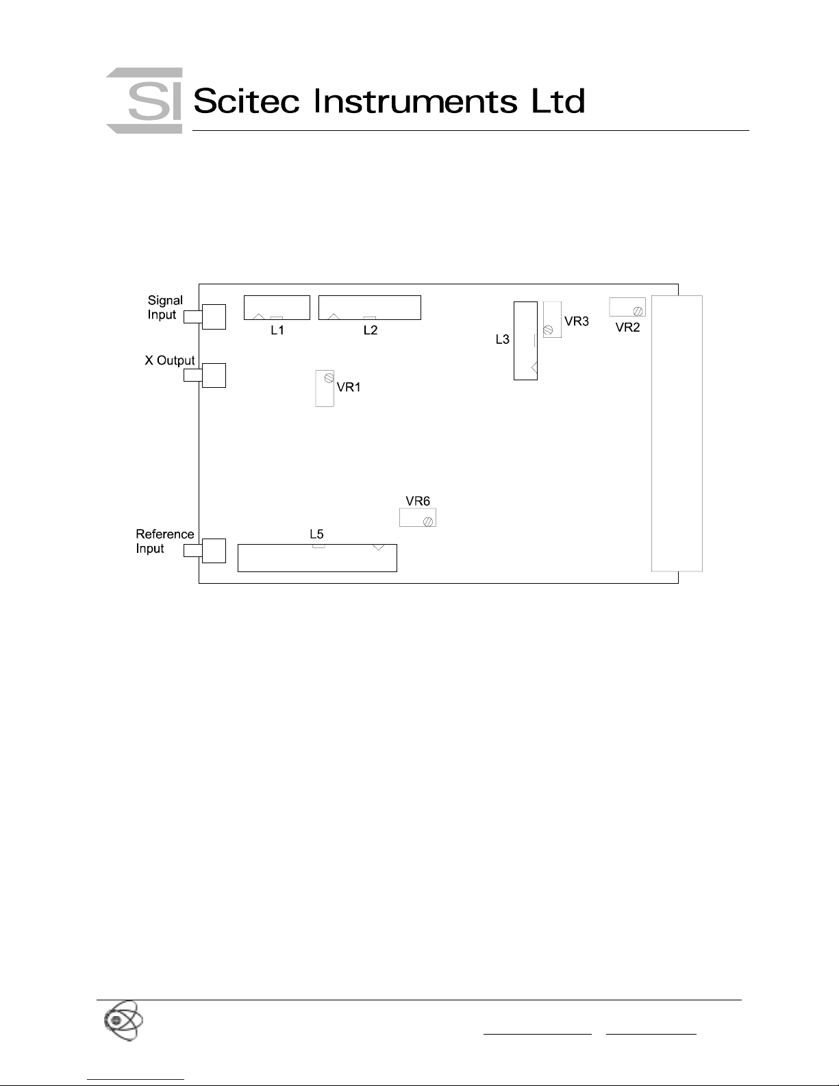
2 BOARD LAYOUT
The 441 board layout is shown in Figure 3.
L1 Input mode selection jumpers
L2 Input gain select jumpers
L3 Channel X output gain select and time constant jumpers
L4 Channel Y output gain select and time constant jumpers
L5 Reference channel mode select jumpers
VR1 Signal feed thro ugh t rim pot
VR2 Channel X offset adjust trim pot
VR3 Channel X gain adjust trim pot
VR4 Channel Y offset adjust trim pot
VR5 Channel Y gain adjust trim pot
VR6 0° - 150° fine phase adjust trim pot
Boston Electronics Corporation, 91 Boylston Street, Brookline MA 02445
(800)347-5445 or (617)566-3821 * fax (617)731-0935 * boselec@boselec.com * www.boselec.com
Figure 3 441 Board Layout
Bartles Industrial Estate Tel: +44 (0)1209 314 608 scitec@scitec.uk.com
North Street, Redruth Fax: +44 (0)1209 314 609 www.scitec.uk.com
Cornwall TR15 1HR Fax2: +44 (0)870 1600 860
The 430 board layout is shown in Figure 4.
Figure 4 430 Board Layout
L1 Input mode selection jumpers
L2 Input gain select jumpers
L3 Channel X output gain select and time constant jumpers
L5 Reference channel mode select jumpers
VR1 Signal feed thro ugh t rim pot
VR2 Channel X offset adjust trim pot
VR3 Channel X gain adjust trim pot
VR6 0° - 150° fine phase adjust trim pot
Boston Electronics Corporation, 91 Boylston Street, Brookline MA 02445
(800)347-5445 or (617)566-3821 * fax (617)731-0935 * boselec@boselec.com * www.boselec.com
Bartles Industrial Estate Tel: +44 (0)1209 314 608 scitec@scitec.uk.com
North Street, Redruth Fax: +44 (0)1209 314 609 www.scitec.uk.com
Cornwall TR15 1HR Fax2: +44 (0)870 1600 860
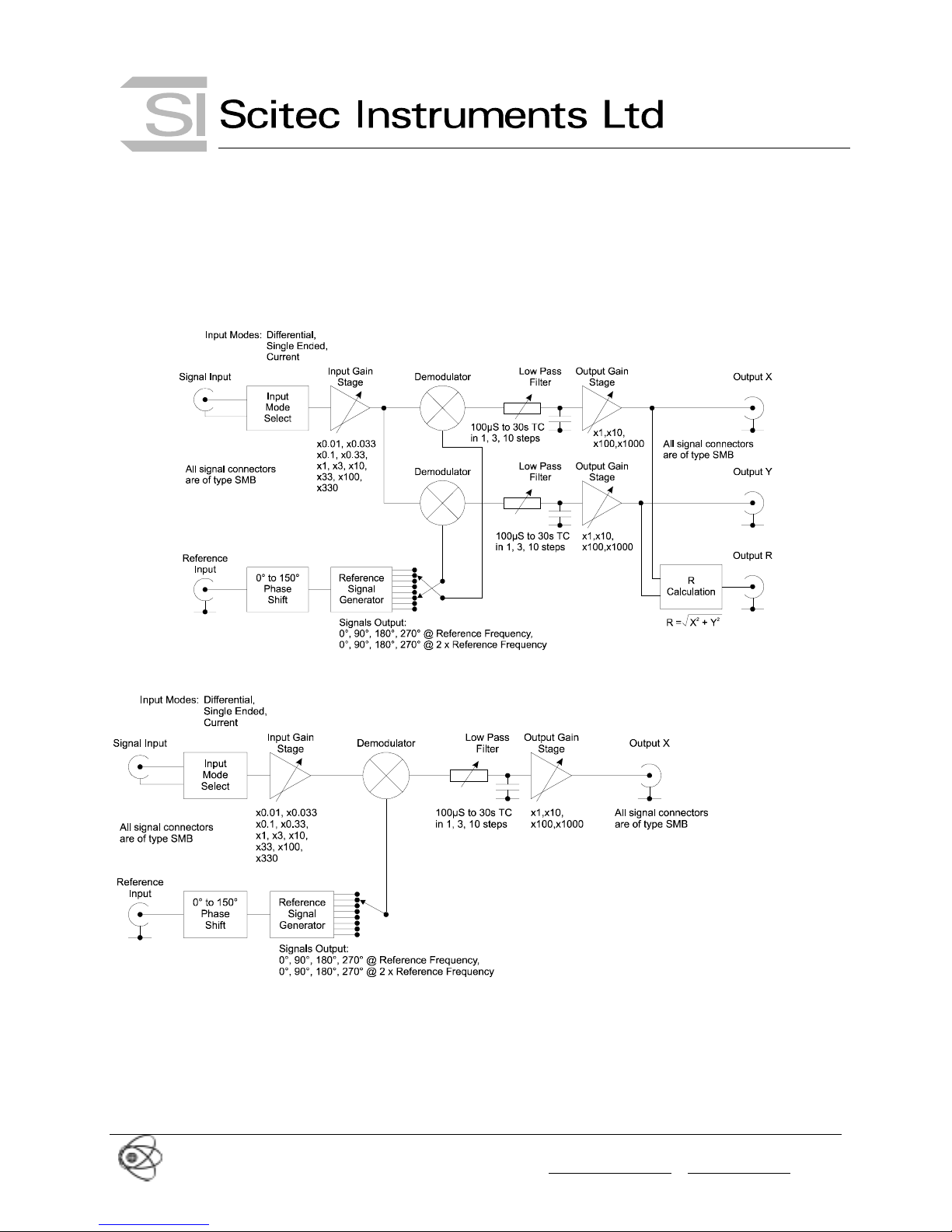
3 OPERATION
3.1 Block Diagrams
Figure 5 441 Block Diagram
Figure 6 430 Block Diagram
3.2 Lock-in Amplifier Theory
For lock-in amplifier theory please visit a number of pages on the Internet produced by M.
Stachel of Faculty of Physics University of Konstanz Germany. It is available at
Boston Electronics Corporation, 91 Boylston Street, Brookline MA 02445
(800)347-5445 or (617)566-3821 * fax (617)731-0935 * boselec@boselec.com * www.boselec.com

Bartles Industrial Estate Tel: +44 (0)1209 314 608 scitec@scitec.uk.com
North Street, Redruth Fax: +44 (0)1209 314 609 www.scitec.uk.com
Cornwall TR15 1HR Fax2: +44 (0)870 1600 860
http://fp.physik.uni-konstanz.de/LockIn/indexx.shtml and includes theory, diagrams and a
virtual Java lock-in amplifier.
Boston Electronics Corporation, 91 Boylston Street, Brookline MA 02445
(800)347-5445 or (617)566-3821 * fax (617)731-0935 * boselec@boselec.com * www.boselec.com
Bartles Industrial Estate Tel: +44 (0)1209 314 608 scitec@scitec.uk.com
North Street, Redruth Fax: +44 (0)1209 314 609 www.scitec.uk.com
Cornwall TR15 1HR Fax2: +44 (0)870 1600 860
4 INPUT STAGE
The input stage amplifies the input signal to a level suitable for the demodulator section.
The input signal should be connected to the SMB signal input connector.
The input sensitivity is set by using the input sensitivity jumpers.
The input stage of the unit can operate in a number of ways. By default, the unit is factory set so
that the input stage acts as a single ended DC coupled input as this is the lowest noise method
of operation. It is also possible to operate the input stage in AC coupled mode, differential
mode and current mode. To operate the lock-in in these different modes requires jumpers on the
unit to be modified. This can be achieved as follows:
4.1 Jumper Settings Overview
A simplified input stage circuit diagram is shown in Figure 7. This shows all of the jumpers in
the input stage.
These jumpers are part of jumper block L1.
Boston Electronics Corporation, 91 Boylston Street, Brookline MA 02445
(800)347-5445 or (617)566-3821 * fax (617)731-0935 * boselec@boselec.com * www.boselec.com
Figure 7 Input Stage Jumper Options

Bartles Industrial Estate Tel: +44 (0)1209 314 608 scitec@scitec.uk.com
North Street, Redruth Fax: +44 (0)1209 314 609 www.scitec.uk.com
Cornwall TR15 1HR Fax2: +44 (0)870 1600 860
4.2 Single Ended DC Coupled Input
The default setting is for a single ended DC coupled input. This mode gives the best noise
performance. Although the input is DC coupled, the input will not saturate with up to the
following DC offsets on the input:
Input Gain Setting Maximum DC Input Offset Before
x0.001 to x3.3 ±10V
x10 to x100 ±1V
x330 ±300mV
The input impedance of the lock-in in this mode is 1012Ω ||1nF.
The jumper set tings for this mode is given in Figure 8. The equivalent ci rcuit is shown in Figure
9.
Saturation Occurs
Figure 8 Single Ended DC Coupled Input Settings
Figure 9 Single Ended DC Coupled Input Circuit
4.3 Single Ended AC Coupled Input
For applications where large amounts of DC offset are expected on the input, the input stage
can be AC coupled with an RC network. Please note that the high value resistor will add a large
amount of thermal noise to the input. (This mode of operation is common to a lot of other
manufacturer’s lock-in amplifiers. When measuring the input noise of their instruments, it is
standard practice to short the input which has the nice result of removing the thermal noise of
this resistor from their measurements. However, how often do you make measurements with the
input shorted in real life??)
(default setting)
Boston Electronics Corporation, 91 Boylston Street, Brookline MA 02445
(800)347-5445 or (617)566-3821 * fax (617)731-0935 * boselec@boselec.com * www.boselec.com

Bartles Industrial Estate Tel: +44 (0)1209 314 608 scitec@scitec.uk.com
North Street, Redruth Fax: +44 (0)1209 314 609 www.scitec.uk.com
Cornwall TR15 1HR Fax2: +44 (0)870 1600 860
In this mode of operation the input can have up to ±12V DC offset before saturation occurs on
all input gain settings.
The input impedance of the lock-in in this mode is 6. 8x10
6
Ω ||100nF.
The jumper settings for this mode is given in Figure 10. The equivalent circuit is shown in
Figure 11.
Figure 10 Single Ended AC Coupled Settings
Figure 11 Single Ended AC Coupled Circuit
4.4 Single Ended Current Input
The input stage can also be used as a current input due to the high impedance of the input stage
opamps. The current input is converted to a voltage by the 6.8MΩ resistor which has a
tolerance of 1%. This mode of operation has not been fully characterised by Scitec Instruments
and is not guaranteed.
The input impedance of the lock-in in this mode is 6. 8x10
The jumper settings for this mode is given in Figure 12. The equivalent circuit is shown in
Figure 13.
Boston Electronics Corporation, 91 Boylston Street, Brookline MA 02445
(800)347-5445 or (617)566-3821 * fax (617)731-0935 * boselec@boselec.com * www.boselec.com
6
Ω ||1nF.

Bartles Industrial Estate Tel: +44 (0)1209 314 608 scitec@scitec.uk.com
North Street, Redruth Fax: +44 (0)1209 314 609 www.scitec.uk.com
Cornwall TR15 1HR Fax2: +44 (0)870 1600 860
Figure 12 Single Ended Current Input Settings
Figure 13 Single Ended Current Input Circuit
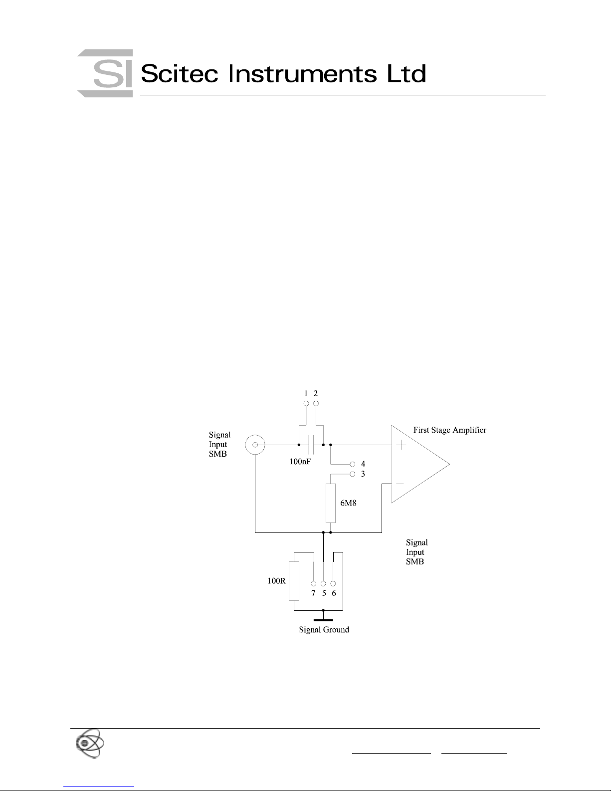
4.5 Differential Input
The above 3 modes can all be converted to a differential input by removing the link between
pins 5 and 6.
It is useful to place the unit into differential mode to avoiding connected the input signal ground
to the lock-in amplifier signal ground. This can be done to break a ground loop or other such
problem.
For example the jumper settings for the Differential DC coupled input are shown in Figure 14
and the equivalent circuit is shown in Figure 15. The other modes are similar.
Please note that it is important that the input signals are not left to float when in differential
mode but are externally coupled to ground by some method. If this is not done, the DC offset
on the input will rise (or fall) until the levels specified in section 4.2 are breached. The input
signal will then be distorted as it travels through the input stage and an erroneous re sult will
occur.
Boston Electronics Corporation, 91 Boylston Street, Brookline MA 02445
(800)347-5445 or (617)566-3821 * fax (617)731-0935 * boselec@boselec.com * www.boselec.com

Bartles Industrial Estate Tel: +44 (0)1209 314 608 scitec@scitec.uk.com
North Street, Redruth Fax: +44 (0)1209 314 609 www.scitec.uk.com
Cornwall TR15 1HR Fax2: +44 (0)870 1600 860
Figure 14 Differential DC Coupled Input Settings
Figure 15 Differential DC Coupled Input Circuit
4.6 Low Impedance Differential Input
If you wish to stop the inputs from floating but do not wish to connect the signals grounds
together then it is possible to achieve this by connecting the grounds together via a 100Ω
resistor by removing the link between pins 5 and 6 and linking pins 5 and 7.
For example the jumper settings for the Low Impedance Differential DC coupled input are
shown in Figure 16 and the equivalent circuit is shown in Figure 17. The other modes are
similar.
Figure 16 Low Impedance Differential DC Coupled Input Settings
Boston Electronics Corporation, 91 Boylston Street, Brookline MA 02445
(800)347-5445 or (617)566-3821 * fax (617)731-0935 * boselec@boselec.com * www.boselec.com
Figure 17 Low Impedance Differential DC Coupled Input Circuit

Bartles Industrial Estate Tel: +44 (0)1209 314 608 scitec@scitec.uk.com
North Street, Redruth Fax: +44 (0)1209 314 609 www.scitec.uk.com
Cornwall TR15 1HR Fax2: +44 (0)870 1600 860
5 FIRST STAGE AMPLIFICATION
A simplified diagram of the input stage amplification is shown in Figure 18. Each stage can
have its gain controlled through the use of jumpers in jump block L2.
Figure 18 Input Stage Amplification
The layout of the pins in L2 are shown in Figure 19. The majority of odd numbered pins are
connected to 0V to reduce noise pickup if a ribbon connector is fitted to L2. Power supply
connections to +15 V and -15 V are also includ ed so that a daught er b oar d ca n be p owere d fro m
the connector.
(Note: Odd numbered pins from 9 to 25 on jump block L2 is a useful place to store unused
jumpers)
Figure 19 L2 Pin Connections
Boston Electronics Corporation, 91 Boylston Street, Brookline MA 02445
(800)347-5445 or (617)566-3821 * fax (617)731-0935 * boselec@boselec.com * www.boselec.com

Bartles Industrial Estate Tel: +44 (0)1209 314 608 scitec@scitec.uk.com
North Street, Redruth Fax: +44 (0)1209 314 609 www.scitec.uk.com
Cornwall TR15 1HR Fax2: +44 (0)870 1600 860
Stage 1 and Stage 3 provide amplification at the input while Stage 2 provides attenuation. The
gain of each stage is set as per the following tables:
Stage 1
Gain Link R
x 1 No link
G1
∞
x 10 pins 2 & 4 5k62
x 33 pins 4 & 6 1k54 The gain in this position can be changed
by changing resistor R3 on the PCB. The
relationship between gain and resistor
value is shown in Figure 18.
Stage 2
Gain Link
x 0.001 pins 10 & 12
x 0.01 pins 12 & 14
x 0.1 pins 16 & 18
x 1 pins 18 & 20 This setting bypasses stage 2 completely
Stage 3
Gain Link R
x 1 No link
G2
∞
x 3.3 pins 22 & 24 21k5
x 10 pins 24 & 26 5k62 The gain in this position can be changed
by changing resistor R13 on the PCB. The
relationship between gain and resistor
value is shown in Figure 18.
By combining the settings in the above tables and overall gain for the input can be generated as
follows:
Nominal Gain Actual Gain Jumper Position
x 0.001 x 0.001004
x 0.00333 x 0.003339
Boston Electronics Corporation, 91 Boylston Street, Brookline MA 02445
(800)347-5445 or (617)566-3821 * fax (617)731-0935 * boselec@boselec.com * www.boselec.com

Bartles Industrial Estate Tel: +44 (0)1209 314 608 scitec@scitec.uk.com
North Street, Redruth Fax: +44 (0)1209 314 609 www.scitec.uk.com
Cornwall TR15 1HR Fax2: +44 (0)870 1600 860
x 0.01 x 0.01006
x 0.0333 x 0.03346
x 0.1 x 0.0996
x 0.333 x 0.3311
x 1 x 1.000
x 3.33 x 3.326
x 10 x 9.90
x 33.3 x 32.91
x 100 x 98.0
x 333 x 325.9
(default)
Boston Electronics Corporation, 91 Boylston Street, Brookline MA 02445
(800)347-5445 or (617)566-3821 * fax (617)731-0935 * boselec@boselec.com * www.boselec.com

Bartles Industrial Estate Tel: +44 (0)1209 314 608 scitec@scitec.uk.com
North Street, Redruth Fax: +44 (0)1209 314 609 www.scitec.uk.com
Cornwall TR15 1HR Fax2: +44 (0)870 1600 860
6 LOW PASS FILTER TIME CONSTANT SETTINGS
The circuit diagram for the time constant section is shown in Figure 20. It consists of a first
order RC low pass filter network with a number of jumper selectable resistor or capacitor
values. Figure 20 shows the circuit for the X channel. The Y channel is identical.
Figure 20 Time Constant and Output Gain Stage Circuit Diagram
6.1 First Time Constant Settings
The jumper positions required for each possible time constant setting are shown in the
following table . The X cha nnel value is set using L3 jump block and the Y channel using L4.
To enable the user to set their own time constant values, resistor R39 (R51 Y channel) and
capacitor C22 (C25 Y channel) are mounted on solder pins.
100µS
300µS
(default)
Boston Electronics Corporation, 91 Boylston Street, Brookline MA 02445
(800)347-5445 or (617)566-3821 * fax (617)731-0935 * boselec@boselec.com * www.boselec.com

Bartles Industrial Estate Tel: +44 (0)1209 314 608 scitec@scitec.uk.com
North Street, Redruth Fax: +44 (0)1209 314 609 www.scitec.uk.com
Cornwall TR15 1HR Fax2: +44 (0)870 1600 860
1mS
3mS
10mS
300mS
1S
3S
100mS
30mS
10S
30S
Boston Electronics Corporation, 91 Boylston Street, Brookline MA 02445
(800)347-5445 or (617)566-3821 * fax (617)731-0935 * boselec@boselec.com * www.boselec.com

Bartles Industrial Estate Tel: +44 (0)1209 314 608 scitec@scitec.uk.com
North Street, Redruth Fax: +44 (0)1209 314 609 www.scitec.uk.com
Cornwall TR15 1HR Fax2: +44 (0)870 1600 860
6.2 Second Time Constant Settings
A second low pass filter stage can be added to the output by mounting capacitor C13 (C14 Y
channel). This capacitor is not normally fitted but allows the production of a faster roll off filter
if required.
The time constant for the second filter is defined as follows:
TimeConstant
= 1.1 x 10⁶ x C13
second
Boston Electronics Corporation, 91 Boylston Street, Brookline MA 02445
(800)347-5445 or (617)566-3821 * fax (617)731-0935 * boselec@boselec.com * www.boselec.com

Bartles Industrial Estate Tel: +44 (0)1209 314 608 scitec@scitec.uk.com
North Street, Redruth Fax: +44 (0)1209 314 609 www.scitec.uk.com
Cornwall TR15 1HR Fax2: +44 (0)870 1600 860
7 OUTPUT STAGE
7.1 Output Stage Amplification
The circuit diagram for the X channel output stage is shown in Figure 20. The Y channel is
identical.
Each channel has 4 output stage amplification settings. The X channel value is set using L3
jump block and the Y channel using L4. The jumper positions required are shown in the
following table.
x 1
Actual
gain =
x 0.91
x 100
Actual
gain =
x 100.9
x 10
Actual
gain =
x 10.9
(default)
The resistor R45 (R54 Y channel) is mounted on solder pillars to enable the gain of the output
stage to be modified. The gain is calculated as follows:
Gain
(Note: the factor of 0.908 occurs in the demodulator section)
7.2 Fine Gain Adjust
The overal l gain of the board c an be adjusted thr ough the fine gain adjust trim potentiomete r
VR3 (VR4 Y channel). This 10 turn trim pot allows adjustment of ±10% of the gain setting.
7.3 Offset Adjust
The DC offset of the system is critical to the overall performance of the board. An offset trim,
VR2 (VR5 Y channel), is included to allow the offset of the system to be adjusted if required.
x 1000
Actual
gain =
x 1000
= (1 + 110K / R45) x 0.908
Output
Boston Electronics Corporation, 91 Boylston Street, Brookline MA 02445
(800)347-5445 or (617)566-3821 * fax (617)731-0935 * boselec@boselec.com * www.boselec.com

Bartles Industrial Estate Tel: +44 (0)1209 314 608 scitec@scitec.uk.com
North Street, Redruth Fax: +44 (0)1209 314 609 www.scitec.uk.com
Cornwall TR15 1HR Fax2: +44 (0)870 1600 860
7.4 R Calculation
The X and Y outputs are combined together by the R calculation circuitry to produce the
modulus of the input signal where R is defined as follows:
Please note that it is important for the X and the Y channels to be noise free before the R
calculation produces the correct value. Due to the squaring calculation, any noise will produce
an additional DC offset to the R output.
Note: The R calculation circuitry is not included on the 430.
7.5 R Calculation Time Constant
A third low pass filter is included in the R calculation circuitry. The time constant for this third
filter is defined as follows:
R = √(X
TimeConstant
2
+ Y2)
= 3.3 x 10⁵ x C19
third
It is important that C19 has a minimum value of 100pF.
Note: The R calculation circuitry is not included on the 430.
8 REFERENCE SECTION
The reference section defines the frequency at which the lock-in recovers signals from the input
channel.
The reference signal is applied to the SMB reference signal input. This input requires a 0-5V
TTL level signal for correct operation.
The reference channel inp ut is rising edge triggered. The falling edge is ignored.
There are a number of jumpers within the reference section which affect the reference signal
before it is passed to the demodulators.
8.1 Fine Phase Control
The first stage of the reference section is a fine phase control circuit. This stage enables the
reference signal to be phase shifted from 0 to approx. 150°. The phase shift is controlled by
VR6.
To enable the fine phase control circuit a jumper needs to be placed between pins 23 and 24 of
jumper block L5 as shown in Figure 21.
Boston Electronics Corporation, 91 Boylston Street, Brookline MA 02445
(800)347-5445 or (617)566-3821 * fax (617)731-0935 * boselec@boselec.com * www.boselec.com

Bartles Industrial Estate Tel: +44 (0)1209 314 608 scitec@scitec.uk.com
North Street, Redruth Fax: +44 (0)1209 314 609 www.scitec.uk.com
Cornwall TR15 1HR Fax2: +44 (0)870 1600 860
Figure 21 Enable Fine Phase Control
To disable the fine phase control circuit and to slightly improve the reference section stability a
jumper needs to be placed between pins 24 and 26 of jumper block L5 as shown in Figure 22.
Figure 22 Disable Fine Phase Control
8.2 Coarse Phase Control and 1F/2F Operation
The Coarse Phase Control allows the reference signal to be phase shifted in multiples of 90°
before it is used by the demodulator. The 1F/2F circuitry multiplies the reference frequency by
1 or by 2. The latter option allows the second harmonic of the input signal to be measured.
(default)
The coarse phase control and the 1F/2F operation is set via the use of jumpers on jumper block
L5 as follows:
Channel X, 1F operation, 0° phase
(default)
shift
Channel X, 1F operation, 90° phase
shift
Channel X, 1F operation, 180° phase
shift
Channel X, 1F operation, 270° phase
shift
Channel X, 2F operation, 0° phase
shift
Channel X, 2F operation, 90° phase
shift
Boston Electronics Corporation, 91 Boylston Street, Brookline MA 02445
(800)347-5445 or (617)566-3821 * fax (617)731-0935 * boselec@boselec.com * www.boselec.com

Bartles Industrial Estate Tel: +44 (0)1209 314 608 scitec@scitec.uk.com
North Street, Redruth Fax: +44 (0)1209 314 609 www.scitec.uk.com
Cornwall TR15 1HR Fax2: +44 (0)870 1600 860
Channel X, 2F operation, 180° phase
shift
Channel X, 2F operation, 270° phase
shift
Channel Y, 1F operation, 0° phase
shift
Channel Y, 1F operation, 90° phase
(default)
shift
Channel Y, 1F operation, 180° phase
shift
Channel Y, 1F operation, 270° phase
shift
Channel Y, 2F operation, 0° phase
shift
Channel Y, 2F operation, 90° phase
shift
Channel Y, 2F operation, 180° phase
shift
Channel Y, 2F operation, 270° phase
shift
Boston Electronics Corporation, 91 Boylston Street, Brookline MA 02445
(800)347-5445 or (617)566-3821 * fax (617)731-0935 * boselec@boselec.com * www.boselec.com

Bartles Industrial Estate Tel: +44 (0)1209 314 608 scitec@scitec.uk.com
North Street, Redruth Fax: +44 (0)1209 314 609 www.scitec.uk.com
Cornwall TR15 1HR Fax2: +44 (0)870 1600 860
9 OVERALL SYSTEM GAIN AND DYNAMIC RESERVE
To get the best performance out of the lock-in amplifier card, it is important that the gain
settings at the input and at the output are correctly balanced to give optimum performance.
A high gain at the input and a low gain at the output improves noise performance and offset
drift. A low gain at the input and a high gai n at the output gives a high dynamic reserve at the
cost of noise and offset performance.
The first stage in achieving optimum performance is to understand the features of the input
signal feed into the lock-in. The different sections are shown in Figure 23.
The input wave form is generally made up from 3 components. They are:
• A sine wave (or similar) at the reference frequency
• Noise at either higher or low frequencies (or both)
• A DC offset
If the DC offset is within the limits specified in Section 4.2 then it can be ignored. If it is
greater than this then it is necessary to AC couple the input, to remove the offset as specified in
Section 4.3.
Boston Electronics Corporation, 91 Boylston Street, Brookline MA 02445
(800)347-5445 or (617)566-3821 * fax (617)731-0935 * boselec@boselec.com * www.boselec.com
Figure 23 Input Signal

Bartles Industrial Estate Tel: +44 (0)1209 314 608 scitec@scitec.uk.com
North Street, Redruth Fax: +44 (0)1209 314 609 www.scitec.uk.com
Cornwall TR15 1HR Fax2: +44 (0)870 1600 860
9.1 Dynamic Reserve
The dynamic reserve of the system is defined as the ratio of the noise to signal that is allowed
within the system before saturation occurs, specified in dBs.
A dynamic reserve of 20dB means that the noise can be a factor of 10 larger than the signal
before saturation occurs.
A dynamic reserve of 40dB means that the noise can be a factor of 100 larger than the signal
before saturation occurs.
A dynamic reserve of 60dB means that the signal can be a factor of 1000 larger than the signal
before saturation occurs.
A dynamic reserve of 80dB means that the signal can be a factor of 10000 larger than the signal
before saturation occurs.
Normally the signal and noise values used to calculate dynamic reserve are RMS
measurements. The following explanation will use the Peak to Peak values as this is easier to
understand and works for all types of noise not just white noise.
9.2 Maximum Signal Size Up To The Low Pass Filter
Assuming that the lock-in amplifier board is operating from ±15V, the maximum Peak to Peak
Signal + Noise amplitude allowed before saturation occurs is 26V. The applies at all stages up
to the input to the Low Pass Filter.
For example, if the input signal fed into the board has a Peak to Peak Signal + Noise value of
100mV, then the maximum gain possible at the inputs stage is 260. If a higher gain than this is
required, then it is necessary to include this additional gain at the output stage. A table of gains
and maximum input signal allowed is given below:
Total Input Stage Gain Maximum Peak to Peak Signal + Noise Input
Allowed Before Saturation Occurs
x 1 26V
x 3.33 7.8V
x 10 2.6V
x 33.3 780mV
x 100 260mV
x 333 78mV
Please note that the maximum gain at the input is not dependant on the amplitude of the signal
you are trying to measure. The maximum gain at the input is only dependant on the amplitude
of the signal + noise.
Boston Electronics Corporation, 91 Boylston Street, Brookline MA 02445
(800)347-5445 or (617)566-3821 * fax (617)731-0935 * boselec@boselec.com * www.boselec.com

Bartles Industrial Estate Tel: +44 (0)1209 314 608 scitec@scitec.uk.com
North Street, Redruth Fax: +44 (0)1209 314 609 www.scitec.uk.com
Cornwall TR15 1HR Fax2: +44 (0)870 1600 860
9.3 Maximum Signal Size From Low Pass F ilter to Output
Once the demodulated signal has pa ssed thro ugh the low pass filter , the noise o n the signal will
be reduced. This reduces the Peak to Peak Signal + Noise amplitude and allows further gain to
be included in the output stage. The maximum size of gain at the output depends on the
amplitude and bandwidth of the noise and also on the time constant of the low pass filter.
Generally, a larger time constant will reduce the noise more allowing a greater output gain to be
used.
9.4 Example Gain Settings
The following is a list of example settings for various input signal and noise levels. This is not
an exhaustive list.
Input Signal Level Input Noise Input Noise
+ Signal
RMS P to P P to P P to P DC
1 V 2.82 V 0 V 2.82 V x 1.14 x 1 x 1 x 1 1 V
1 V 2.82 V 0 V 2.82 V x 9.2 x 3.33 x 1 x 3.33 3.33 V
1 V 2.82 V 0 V 2.82 V x 1.14 x 1 x 10 x 10 10 V
1 V 2.82 V 20 V 22.82 V x 1.14 x 1 x 1 x 1 1 V
1 V 2.82 V 4 V 6.82 V x 3.81 x 3.33 x 1 x 3.33 3.33 V
1 V 2.82 V 20 V 22.82 V x 1.14 x 1 x 10 x 10 10 V
300 mV 848 mV 0 V 848 mV x 30.6 x 1 x 1 x 1 300 mV
300 mV 848 mV 0 V 848 mV x 30.6 x 3.33 x 1 x 3.33 1 V
300 mV 848 mV 0 V 848 mV x 30.6 x 10 x 1 x 10 3 V
300 mV 848 mV 0 V 848 mV x 30.6 x 3.33 x 10 x 33.3 10 V
300 mV 848 mV 20 V 20.9 V x 1.24 x 1 x 1 x 1 300 mV
300 mV 848 mV 6 V 6.85 V x 3.80 x 3.33 x 1 x 3.33 1 V
300 mV 848 mV 2 V 2.85 V x 9.12 x 10 x 1 x 10 3 V
300 mV 848 mV 6 V 6.85 V x 3.80 x 3.33 x 10 x 33.3 10 V
100 mV 282 mV 0 V 282 mV x 92.2 x 1 x 1 x 1 100 mV
100 mV 282 mV 0 V 282 mV x 92.2 x 3.33 x 1 x 3.33 333 mV
100 mV 282 mV 0 V 282 mV x 92.2 x 10 x 1 x 10 1 V
100 mV 282 mV 0 V 282 mV x 92.2 x 33.3 x 1 x 33.3 3.33 V
100 mV 282 mV 0 V 282 mV x 92.2 x 10 x 10 x 100 10 V
100 mV 282 mV 20 V 20.3 V x 1.28 x 1 x 1 x 1 100 mV
100 mV 282 mV 7 V 7.28 V x 3.56 x 3.33 x 1 x 3.33 333 mV
100 mV 282 mV 2 V 2.28 V x 11.4 x 10 x 1 x 10 1 V
100 mV 282 mV 400 mV 682 mV x 38.1 x 33.3 x 1 x 33.3 3.33 V
30 mV 84.8 mV 0V 84.8 mV x 306 x 1 x 1 x 1 30 mV
30 mV 84.8 mV 0V 84.8 mV x 306 x 3.33 x 1 x 3.33 100 mV
30 mV 84.8 mV 0V 84.8 mV x 306 x 10 x 1 x 10 300 mV
30 mV 84.8 mV 0V 84.8 mV x 306 x 33.3 x 1 x 33.3 1 V
30 mV 84.8 mV 0V 84.8 mV x 306 x 100 x 1 x 100 3 V
30 mV 84.8 mV 0V 84.8 mV x 306 x 33.3 x 10 x 333 10 V
30 mV 84.8 mV 0V 84.8 mV x 306 x 3.33 x 100 x 333 10 V
30 mV 84.8 mV 20V 20V x 1.3 x 1 x 1 x 1 30 mV
30 mV 84.8 mV 7V 7.08 V x 3.67 x 3.33 x 1 x 3.33 100 mV
30 mV 84.8 mV 2V 2.08 V x 12.5 x 10 x 1 x 10 300 mV
30 mV 84.8 mV 600 mV 685 mV x 38.0 x 33.3 x 1 x 33.3 1 V
30 mV 84.8 mV 100 mV 185 mV x 141 x 100 x 1 x 100 3 V
30 mV 84.8 mV 600 mV 84.8 mV x 38.0 x 33.3 x 10 x 333 10 V
Maximum
Input Gain
Setting
Actual Input
Gain Setting
Output Gain
Setting
Total System
Gain
Output
Voltage
Boston Electronics Corporation, 91 Boylston Street, Brookline MA 02445
(800)347-5445 or (617)566-3821 * fax (617)731-0935 * boselec@boselec.com * www.boselec.com

Bartles Industrial Estate Tel: +44 (0)1209 314 608 scitec@scitec.uk.com
North Street, Redruth Fax: +44 (0)1209 314 609 www.scitec.uk.com
Cornwall TR15 1HR Fax2: +44 (0)870 1600 860
Input Signal Level Input Noise Input Noise
+ Signal
RMS P to P P to P P to P DC
30 mV 84.8 mV 7 V 7.08 V x 3.67 x 3.33 x 100 x 333 10 V
10 mV 28.2 mV 0 V 28.2 mV x 922 x 1 x 1 x 1 10 mV
10 mV 28.2 mV 0 V 28.2 mV x 922 x 3.33 x 1 x 3.33 33.3 mV
10 mV 28.2 mV 0 V 28.2 mV x 922 x 10 x 1 x 10 100 mV
10 mV 28.2 mV 0 V 28.2 mV x 922 x 33.3 x 1 x 33.3 333 mV
10 mV 28.2 mV 0 V 28.2 mV x 922 x 100 x 1 x 100 1 V
10 mV 28.2 mV 0 V 28.2 mV x 922 x 333 x 1 x 333 3.33 V
10 mV 28.2 mV 0 V 28.2 mV x 922 x 100 x 10 x 1000 10 V
10 mV 28.2 mV 0 V 28.2 mV x 922 x 10 x 100 x 1000 10 V
10 mV 28.2 mV 0 V 28.2 mV x 922 x 1 x 1000 x 1000 10 V
10 mV 28.2 mV 20 V 20 V x 1.3 x 1 x 1 x 1 10 mV
10 mV 28.2 mV 7 V 7.02 V x 3.7 x 3.33 x 1 x 3.33 33.3 mV
10 mV 28.2 mV 2 V 2.02V x 12.9 x 10 x 1 x 10 100 mV
10 mV 28.2 mV 700 mV 728 mV x 35.7 x 33.3 x 1 x 33.3 333 mV
10 mV 28.2 mV 200 mV 228 mV x 114 x 100 x 1 x 100 1 V
10 mV 28.2 mV 40 mV 68.2 mV x 381 x 333 x 1 x 333 3.33 V
10 mV 28.2 mV 200 mV 228 mV x 114 x 100 x 10 x 1000 10 V
10 mV 28.2 mV 2 V 2.02 V x 12.9 x 10 x 100 x 1000 10 V
10 mV 28.2 mV 20 V 20 V x 1.3 x 1 x 1000 x 1000 10 V
3 mV 8.48 mV 0 V 8.48 mV x 3070 x 1 x 1 x 1 3 mV
3 mV 8.48 mV 0 V 8.48 mV x 3070 x 3.33 x 1 x 3.33 10 mV
3 mV 8.48 mV 0 V 8.48 mV x 3070 x 10 x 1 x 10 30 mV
3 mV 8.48 mV 0 V 8.48 mV x 3070 x 33.3 x 1 x 33.3 100 mV
3 mV 8.48 mV 0 V 8.48 mV x 3070 x 100 x 1 x 100 300 mV
3 mV 8.48 mV 0 V 8.48 mV x 3070 x 333 x 1 x 333 1 V
3 mV 8.48 mV 0 V 8.48 mV x 3070 x 100 x 10 x 1000 3 V
3 mV 8.48 mV 0 V 8.48 mV x 3070 x 333 x 10 x 3330 10 V
3 mV 8.48 mV 0 V 8.48 mV x 3070 x 33.3 x 100 x 3330 10 V
3 mV 8.48 mV 0 V 8.48 mV x 3070 x 3.33 x 1000 x 3330 10 V
3 mV 8.48 mV 20 V 20 V x 1.3 x 1 x 1 x 1 3 mV
3 mV 8.48 mV 7 V 7 V x 3.7 x 3.33 x 1 x 3.33 10 mV
3 mV 8.48 mV 2 V 2 V x 13 x 10 x 1 x 10 30 mV
3 mV 8.48 mV 700 mV 708 mV x 36.7 x 33.3 x 1 x 33.3 100 mV
3 mV 8.48 mV 200 mV 208 mV x 125 x 100 x 1 x 100 300 mV
3 mV 8.48 mV 60 mV 68.5 mV x 380 x 333 x 1 x 333 1 V
3 mV 8.48 mV 200 mV 208 mV x 125 x 100 x 10 x 1000 3 V
3 mV 8.48 mV 60 mV 68.5 mV x 380 x 333 x 10 x 3330 10 V
3 mV 8.48 mV 700 mV 708 mV x 36.7 x 33.3 x 100 x 3330 10 V
3 mV 8.48 mV 7 V 7 V x 3.7 x 3.33 x 1000 x 3330 10 V
1 mV 2.82 mV 0 V 2.82 mV - x 1 x 1 x 1 1 mV
1 mV 2.82 mV 0 V 2.82 mV - x 3.33 x 1 x 3.33 3.33 mV
1 mV 2.82 mV 0 V 2.82 mV - x 10 x 1 x 10 10 mV
1 mV 2.82 mV 0 V 2.82 mV - x 33.3 x 1 x 33.3 33.3 mV
1 mV 2.82 mV 0 V 2.82 mV - x 100 x 1 x 100 100 mV
1 mV 2.82 mV 0 V 2.82 mV - x 333 x 1 x 333 333 mV
1 mV 2.82 mV 0 V 2.82 mV - x 100 x 10 x 1000 1 V
1 mV 2.82 mV 0 V 2.82 mV - x 333 x 10 x 3330 3.33 V
1 mV 2.82 mV 0 V 2.82 mV - x 100 x 100 x 10000 10 V
1 mV 2.82 mV 0 V 2.82 mV - x 10 x 1000 x 10000 10 V
1 mV 2.82 mV 20 V 20 V x 1.3 x 1 x 1 x 1 1 mV
1 mV 2.82 mV 7 V 7 V x 3.7 x 3.33 x 1 x 3.33 3.33 mV
Maximum
Input Gain
Setting
Actual Input
Gain Setting
Output Gain
Setting
Total System
Gain
Output
Voltage
Boston Electronics Corporation, 91 Boylston Street, Brookline MA 02445
(800)347-5445 or (617)566-3821 * fax (617)731-0935 * boselec@boselec.com * www.boselec.com

Bartles Industrial Estate Tel: +44 (0)1209 314 608 scitec@scitec.uk.com
North Street, Redruth Fax: +44 (0)1209 314 609 www.scitec.uk.com
Cornwall TR15 1HR Fax2: +44 (0)870 1600 860
Input Signal Level Input Noise Input Noise
+ Signal
RMS P to P P to P P to P DC
1 mV 2.82 mV 2 V 2 V x 13 x 10 x 1 x 10 10 mV
1 mV 2.82 mV 700 mV 703 mV x 37.0 x 33.3 x 1 x 33.3 33.3 mV
1 mV 2.82 mV 200 mV 203 mV x 128 x 100 x 1 x 100 100 mV
1 mV 2.82 mV 70 mV 72.8 mV x 357 x 333 x 1 x 333 333 mV
1 mV 2.82 mV 200 mV 203 mV x 128 x 100 x 10 x 1000 1 V
1 mV 2.82 mV 70 mV 72.8 mV x 357 x 333 x 10 x 3330 3.33 V
1 mV 2.82 mV 200 mV 203 mV x 128 x 100 x 100 x 10000 10 V
1 mV 2.82 mV 2 V 2 V x 13 x 10 x 1000 x 10000 10 V
300 µV 848 µV 0 V 848 µV - x 1 x 1 x 1 300 µV
300 µV 848 µV 0 V 848 µV - x 3.33 x 1 x 3.33 1 mV
300 µV 848 µV 0 V 848 µV - x 10 x 1 x 10 3.33 mV
300 µV 848 µV 0 V 848 µV - x 33.3 x 1 x 33.3 10 mV
300 µV 848 µV 0 V 848 µV - x 100 x 1 x 100 33.3 mV
300 µV 848 µV 0 V 848 µV - x 333 x 1 x 333 100 mV
300 µV 848 µV 0 V 848 µV - x 100 x 10 x 1000 333 mV
300 µV 848 µV 0 V 848 µV - x 333 x 10 x 3330 1 V
300 µV 848 µV 0 V 848 µV - x 100 x 100 x 10000 3.33 V
300 µV 848 µV 0 V 848 µV - x 333 x 100 x 33300 10 V
300 µV 848 µV 0 V 848 µV - x 33.3 x 1000 x 33300 10 V
300 µV 848 µV 20 V 20 V x 1.3 x 1 x 1 x 1 300 µV
300 µV 848 µV 7 V 7 V x 3.7 x 3.33 x 1 x 3.33 1 mV
300 µV 848 µV 2 V 2 V x 13 x 10 x 1 x 10 3 mV
300 µV 848 µV 700 mV 700 mV x 37.0 x 33.3 x 1 x 33.3 10 mV
300 µV 848 µV 200 mV 200 mV x 128 x 100 x 1 x 100 30 mV
300 µV 848 µV 70 mV 70.8 mV x 367 x 333 x 1 x 333 100 mV
300 µV 848 µV 200 mV 200 mV x 128 x 100 x 10 x 1000 300 mV
300 µV 848 µV 70 mV 70.8 mV x 367 x 333 x 10 x 3330 1 V
300 µV 848 µV 200 mV 200 mV x 128 x 100 x 100 x 10000 3 V
300 µV 848 µV 70 mV 70.8 mV x 367 x 333 x 100 x 33300 10 V
300 µV 848 µV 700 mV 700 mV x 37.0 x 33.3 x 1000 x 33300 10 V
100 µV 282 µV 0V 282 µV - x 1 x 1 x 1 100 µV
100 µV 282 µV 0V 282 µV - x 3.33 x 1 x 3.33 333 µV
100 µV 282 µV 0V 282 µV - x 10 x 1 x 10 1 mV
100 µV 282 µV 0V 282 µV - x 33.3 x 1 x 33.3 3.33 mV
100 µV 282 µV 0V 282 µV - x 100 x 1 x 100 10 mV
100 µV 282 µV 0V 282 µV - x 333 x 1 x 333 33.3 mV
100 µV 282 µV 0V 282 µV - x 100 x 10 x 1000 100 mV
100 µV 282 µV 0V 282 µV - x 333 x 10 x 3330 333 mV
100 µV 282 µV 0V 282 µV - x 100 x 100 x 10000 1 V
100 µV 282 µV 0V 282 µV - x 333 x 100 x 33300 3.33 V
100 µV 282 µV 0V 282 µV - x 100 x 1000 x 100000 10 V
100 µV 282 µV 20 V 20 V x 1.3 x 1 x 1 x 1 100 µV
100 µV 282 µV 7 V 7 V x 3.7 x 3.33 x 1 x 3.33 333 µV
100 µV 282 µV 2 V 2 V x 13 x 10 x 1 x 10 1 mV
100 µV 282 µV 700 mV 700 mV x 37.0 x 33.3 x 1 x 33.3 3.33 mV
100 µV 282 µV 200 mV 200 mV x 128 x 100 x 1 x 100 10 mV
100 µV 282 µV 70 mV 70.3 mV x 370 x 333 x 1 x 333 33.3 mV
100 µV 282 µV 200 mV 200 mV x 128 x 100 x 10 x 1000 100 mV
100 µV 282 µV 70 mV 70.3 mV x 370 x 333 x 10 x 3330 333 mV
100 µV 282 µV 200 mV 200 mV x 128 x 100 x 100 x 10000 1 V
100 µV 282 µV 70 mV 70.3 mV x 370 x 333 x 100 x 33300 3.33 V
Maximum
Input Gain
Setting
Actual Input
Gain Setting
Output Gain
Setting
Total System
Gain
Output
Voltage
Boston Electronics Corporation, 91 Boylston Street, Brookline MA 02445
(800)347-5445 or (617)566-3821 * fax (617)731-0935 * boselec@boselec.com * www.boselec.com

Bartles Industrial Estate Tel: +44 (0)1209 314 608 scitec@scitec.uk.com
North Street, Redruth Fax: +44 (0)1209 314 609 www.scitec.uk.com
Cornwall TR15 1HR Fax2: +44 (0)870 1600 860
Input Signal Level Input Noise Input Noise
+ Signal
RMS P to P P to P P to P DC
100 µV 282 µV 200 mV 200 mV x 128 x 100 x 1000 x 100000 10 V
30 µV 84.8 µV 0 V 84.8 µV - x 1 x 1 x 1 30 µV
30 µV 84.8 µV 0 V 84.8 µV - x 3.33 x 1 x 3.33 100 µV
30 µV 84.8 µV 0 V 84.8 µV - x 10 x 1 x 10 333 µV
30 µV 84.8 µV 0 V 84.8 µV - x 33.3 x 1 x 33.3 1 mV
30 µV 84.8 µV 0 V 84.8 µV - x 100 x 1 x 100 3.33 mV
30 µV 84.8 µV 0 V 84.8 µV - x 333 x 1 x 333 10 mV
30 µV 84.8 µV 0 V 84.8 µV - x 100 x 10 x 1000 33.3 mV
30 µV 84.8 µV 0 V 84.8 µV - x 333 x 10 x 3330 100 mV
30 µV 84.8 µV 0 V 84.8 µV - x 100 x 100 x 10000 333 mV
30 µV 84.8 µV 0 V 84.8 µV - x 333 x 100 x 33300 1 V
30 µV 84.8 µV 0 V 84.8 µV - x 100 x 1000 x 100000 3.33 V
30 µV 84.8 µV 0 V 84.8 µV - x 333 x 1000 x 333000 10 V
30 µV 84.8 µV 20 V 20 V x 1.3 x 1 x 1 x 1 30 µV
30 µV 84.8 µV 7 V 7 V x 3.7 x 3.33 x 1 x 3.33 100 µV
30 µV 84.8 µV 2 V 2 V x 13 x 10 x 1 x 10 300 µV
30 µV 84.8 µV 700 mV 700 mV x 37.0 x 33.3 x 1 x 33.3 1 mV
30 µV 84.8 µV 200 mV 200 mV x 128 x 100 x 1 x 100 3 mV
30 µV 84.8 µV 70 mV 70 mV x 370 x 333 x 1 x 333 10 mV
30 µV 84.8 µV 200 mV 200 mV x 128 x 100 x 10 x 1000 30 mV
30 µV 84.8 µV 70 mV 70 mV x 370 x 333 x 10 x 3330 100 mV
30 µV 84.8 µV 200 mV 200 mV x 128 x 100 x 100 x 10000 300 mV
30 µV 84.8 µV 70 mV 70 mV x 370 x 333 x 100 x 33300 1 V
30 µV 84.8 µV 200 mV 200 mV x 128 x 100 x 1000 x 100000 3 V
30 µV 84.8 µV 70 mV 70 mV x 370 x 333 x 1000 x 333000 10 V
10 µV 28.2 µV 0 V 28.2 µV - x 1 x 1 x 1 10 µV
10 µV 28.2 µV 0 V 28.2 µV - x 3.33 x 1 x 3.33 33.3 µV
10 µV 28.2 µV 0 V 28.2 µV - x 10 x 1 x 10 100 µV
10 µV 28.2 µV 0 V 28.2 µV - x 33.3 x 1 x 33.3 333 µV
10 µV 28.2 µV 0 V 28.2 µV - x 100 x 1 x 100 1 mV
10 µV 28.2 µV 0 V 28.2 µV - x 333 x 1 x 333 3.33 mV
10 µV 28.2 µV 0 V 28.2 µV - x 100 x 10 x 1000 10 mV
10 µV 28.2 µV 0 V 28.2 µV - x 333 x 10 x 3330 33.3 mV
10 µV 28.2 µV 0 V 28.2 µV - x 100 x 100 x 10000 100 mV
10 µV 28.2 µV 0 V 28.2 µV - x 333 x 100 x 33300 333 mV
10 µV 28.2 µV 0 V 28.2 µV - x 100 x 1000 x 100000 1 V
10 µV 28.2 µV 0 V 28.2 µV - x 333 x 1000 x 333000 3.33 V
10 µV 28.2 µV 20 V 20 V x 1.3 x 1 x 1 x 1 10 µV
10 µV 28.2 µV 7 V 7 V x 3.7 x 3.33 x 1 x 3.33 33.3 µV
10 µV 28.2 µV 2 V 2 V x 13 x 10 x 1 x 10 100 µV
10 µV 28.2 µV 700 mV 700 mV x 37.0 x 33.3 x 1 x 33.3 333 µV
10 µV 28.2 µV 200 mV 200 mV x 128 x 100 x 1 x 100 1 mV
10 µV 28.2 µV 70 mV 70 mV x 370 x 333 x 1 x 333 3.33 mV
10 µV 28.2 µV 200 mV 200 mV x 128 x 100 x 10 x 1000 10 mV
10 µV 28.2 µV 70 mV 70 mV x 370 x 333 x 10 x 3330 33.3 mV
10 µV 28.2 µV 200 mV 200 mV x 128 x 100 x 100 x 10000 100 mV
10 µV 28.2 µV 70 mV 70 mV x 370 x 333 x 100 x 33300 333 mV
10 µV 28.2 µV 200 mV 200 mV x 128 x 100 x 1000 x 100000 1 V
10 µV 28.2 µV 70 mV 70 mV x 370 x 333 x 1000 x 333000 3.33 V
3 µV 8.48 µV 0 V 8.48 µV - x 1 x 1 x 1 3 µV
3 µV 8.48 µV 0 V 8.48 µV - x 3.33 x 1 x 3.33 10 µV
Maximum
Input Gain
Setting
Actual Input
Gain Setting
Output Gain
Setting
Total System
Gain
Output
Voltage
Boston Electronics Corporation, 91 Boylston Street, Brookline MA 02445
(800)347-5445 or (617)566-3821 * fax (617)731-0935 * boselec@boselec.com * www.boselec.com

Bartles Industrial Estate Tel: +44 (0)1209 314 608 scitec@scitec.uk.com
North Street, Redruth Fax: +44 (0)1209 314 609 www.scitec.uk.com
Cornwall TR15 1HR Fax2: +44 (0)870 1600 860
Input Signal Level Input Noise Input Noise
+ Signal
RMS P to P P to P P to P DC
3 µV 8.48 µV 0 V 8.48 µV - x 10 x 1 x 10 30 µV
3 µV 8.48 µV 0 V 8.48 µV - x 33.3 x 1 x 33.3 100 µV
3 µV 8.48 µV 0 V 8.48 µV - x 100 x 1 x 100 300 µV
3 µV 8.48 µV 0 V 8.48 µV - x 333 x 1 x 333 1 mV
3 µV 8.48 µV 0 V 8.48 µV - x 100 x 10 x 1000 3 mV
3 µV 8.48 µV 0 V 8.48 µV - x 333 x 10 x 3330 10 mV
3 µV 8.48 µV 0 V 8.48 µV - x 100 x 100 x 10000 30 mV
3 µV 8.48 µV 0 V 8.48 µV - x 333 x 100 x 33300 100 mV
3 µV 8.48 µV 0 V 8.48 µV - x 100 x 1000 x 100000 300 mV
3 µV 8.48 µV 0 V 8.48 µV - x 333 x 1000 x 333000 1 V
3 µV 8.48 µV 20 V 20 V x 1.3 x 1 x 1 x 1 3 µV
3 µV 8.48 µV 7 V 7 V x 3.7 x 3.33 x 1 x 3.33 10 µV
3 µV 8.48 µV 2 V 2 V x 13 x 10 x 1 x 10 30 µV
3 µV 8.48 µV 700 mV 700 mV x 37.0 x 33.3 x 1 x 33.3 100 µV
3 µV 8.48 µV 200 mV 200 mV x 128 x 100 x 1 x 100 300 µV
3 µV 8.48 µV 70 mV 70 mV x 370 x 333 x 1 x 333 1 mV
3 µV 8.48 µV 200 mV 200 mV x 128 x 100 x 10 x 1000 3 mV
3 µV 8.48 µV 70 mV 70 mV x 370 x 333 x 10 x 3330 10 mV
3 µV 8.48 µV 200 mV 200 mV x 128 x 100 x 100 x 10000 30 mV
3 µV 8.48 µV 70 mV 70 mV x 370 x 333 x 100 x 33300 100 mV
3 µV 8.48 µV 200 mV 200 mV x 128 x 100 x 1000 x 100000 300 mV
3 µV 8.48 µV 70 mV 70 mV x 370 x 333 x 1000 x 333000 1 V
Maximum
Input Gain
Setting
Actual Input
Gain Setting
Output Gain
Setting
Total System
Gain
Output
Voltage
Boston Electronics Corporation, 91 Boylston Street, Brookline MA 02445
(800)347-5445 or (617)566-3821 * fax (617)731-0935 * boselec@boselec.com * www.boselec.com
 Loading...