

Page 1

CV512H-U42 Service Manual
INPUT
ATV (Analog PAL/SECAM),DTV (DVB-T2/T/C)
1
DTV (DVB-S2)
-
Mini YpbPr/RCA YPbpr
1
Mini AV In(CVBS -PAL/NTSC + L,R)
-
SCART/RCA AV IN
1
PC In (RGB/H/V + L/R)
1
USB2.0 (MP3/JPEG/RMVB)
2
HDMI In (HDMI-1.4a)
3
COAX/OPTICAL
1
CV512H-U 42 after-sales support and maintenance manual
CV512H- U42 is a power supply, constant current driver, one of the TV boards, may receive a PAL /
SECAM standard analog television signal, for European (including UK) and other
markets. CV512H-U42 used in high efficiency switching power supply, matching backlight
power 45 W or less, typically a voltage value matching the backlight 45 V ~ 100V, dual backlight
parallel output, -42 inch to 32-inch LED backlight screen.
1. the safety instructions:
1.1 replacement, any welding components when the dial plug and cable, power supply must be
OFF.
a) BULK capacitor needs to discharge
b) can not be touched once after power on
1.2 anti-static measures (the entire production process must be anti-static!)
a) can not easily touch the IC;
b) an anti-static iron;
c) welder must wear anti-static gloves.
1.3 replacement of components that have special safety requirements, reference list should not be
free to change specifications and models.
1.4 Test and verify the board must use the matching accessories (power board, keypad, etc.), if you
use other accessories need to carefully confirm the correctness of the connection.
1.5 board storage, the use of temperature and humidity are as follows, be sure to strictly follow
the implementation:
Storage temperature / humidity: -40 ~ + 85 ℃ <= 95%.
Temperature / humidity: - 1 0 + 60 ℃. <= 95%
Note: Observe the safety instructions as described above when servicing this motherboard.
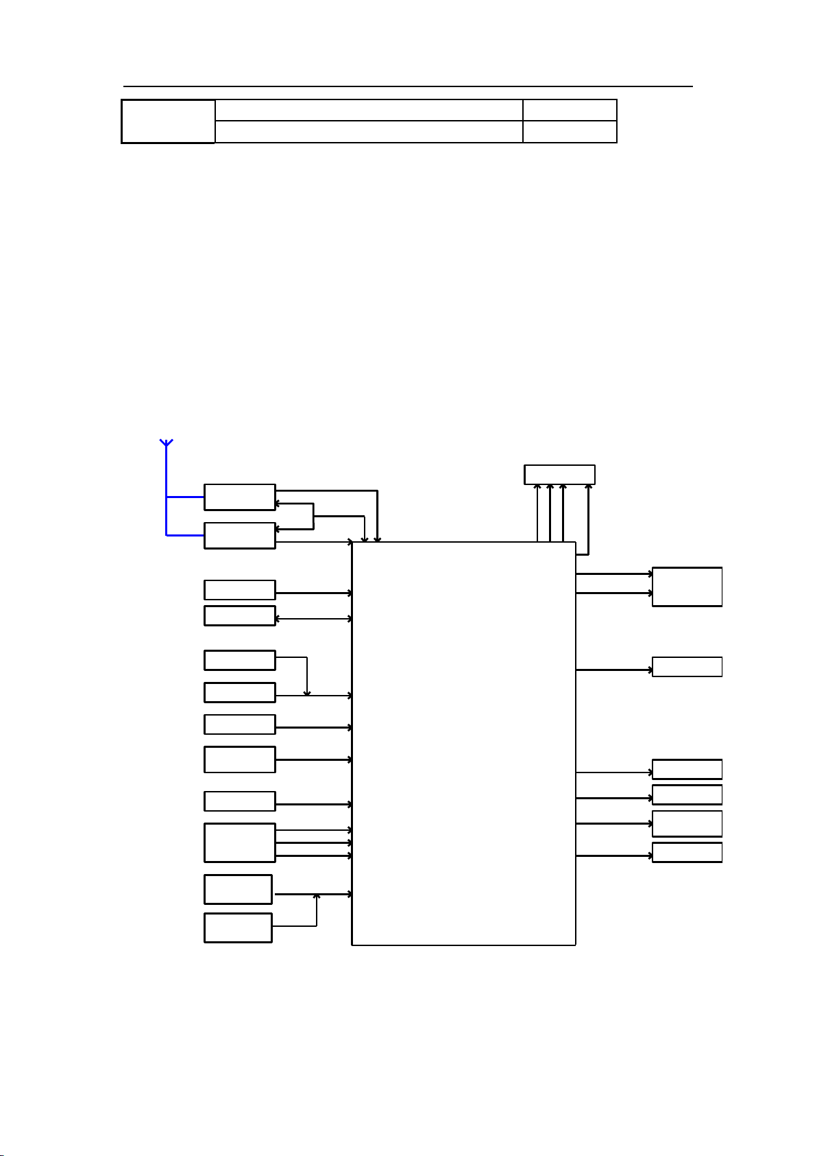
2. the main function:
1. Supports SD and HD resolutions (480P / 576i / 720p / 1080i / 1080P);
2. Low standby power (≤ 0.5 W)
3. Input/Output ports:
Page 2
CV512H-U42 Service Manual
OUTPUT
Audio Out (L,R)
1
EARPHONE (L,R)
1
ANTENNA
CVBS2
HDMI2 WITH MHL
RGB
4 M Byte
DVB-T2/T/C/S2
S2T512
R/L Audio
VGA(PC)
IR/KEYPAD
INTERFACE
Dual LVDS 10BIT
SPDIF
USB 2.0*2
CODE FLASH
USB*2
CI_CARD
YPBPR*2
MP7752
LINE_OUT
AV1&2
1920x1080
TS X8
I2C
CI_DATA X8
CI_ADD X12
PANEL
H/VSYNC
CATS X8
CVBS1
YPBPR1
EARPHONE
LINE_OUT
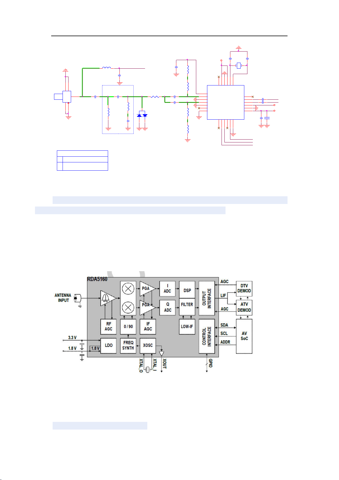
RDA5160
HP_L/R
HDMI*3
LINE_IN x 3
HDMI1 WITH ARC
IF/IQ
DVD R/L
SCART R/L
PC R/L
AV1 R/L
CVBSOUT
CVBSOUT
DIO1717
SPDIF
SGM331
DVD YPbPr
Scart RGB
HDMI3
RDA5815M
IF_IN/IF_IP/IF_QN/IF_QP
4. 32 bit processor, built 128MB DDR3;
5. Support USB software upgrade;
3. the basic working principle:
(1) analog signal flow:
Signal received by the antenna into the TUNER (UT1, RDA5160; U27, RDA5815), SOC
(U7 S2T512) by the TUNER I2C control, frequency selection, setting IF bandwidth, the amplitude of
the intermediate frequency signal is provided. TUNER output IF signal into the SOC internal
demodulation and decoding, and ultimately converted into video and audio signal display.
(2) Basic block diagram:
(3) Power composition:
Page 3
CV512H-U42 Service Manual
3.3VU(75mA)5VU
LP3992
FOR S2T512
220V AV~
TPS563201
12VU
SMPS
TLV62565
12VU(1000mA)
TLV62569
3118e
LP3983
1.24V(1970mA)
FOR S2T512
FOR DDR
FOR S2T512
3.3VA(280mA)
220mA
1.5VA(215mA)
FOR RDA5815
155mA
FOR RDA5160
AMP
S2
T2/T/C
FOR LNB
带DVD功能上4A DCDC
FOR flash
500mA
TPS2065DDBVR
FOR ANT
3.3V_TUNER
FOR USB
TPS2065DDBVR
EN
GV3407
FOR DVD
GV3407
S805安卓小板
FOR PANEL
GV3407
0R
0R
1000mA
1000mA
500mA
5VU
EN
EN
3.3VA
900mA
FOR MHL
SGM2588
12VU
5VU
3.3VA
FB2
FB120R/ 3A
NC
CD2 10uF/6. 3V
CD6 10uF/6. 3V
RD4
12K_1%
CD3 10uF/6. 3V
12VU
CD4 10uF/6. 3V
CD5 100nF/16V
CD9 100nF/ 16V
TP1
5VU
1
5VU
UD1
TPS563201
VBST
6
GND
1
VFB
4
EN
5
VIN
3
SW
2
RD2 100K
RD1
68K_1%
3A
CD8 10uF /16V
CD1 100nF/16V
R2
R1
Vout=0.768*(1+R1/R2)
LD1
4.7uH/ 6A
RD3 NC/18K
NC
+12V
+5V_Standby POWER 3A
CV 512H-U50 power architecture of FIG.
(4). Specific circuit analysis
(a) 12V 5V switch circuit :
Page 4
CV512H-U42 Service Manual
CD17
NC/100nF/ 16V
1V_EN
UD2
TLV62569
IN4SW
3
GND
2
EN1FB
5
CD12 10uF/6. 3V
CD10 10uF/6. 3V
CD14 100nF/ 16V
RD6
13K_1%
RD510K
LD2 2.2uH/ 2.2A
CD11 100nF/16V
RD8
12K_1%
CD13 10uF/6. 3V
R2
R1
V_1V
5VU
Vout= 0.6*(1+R1/R2) 2A
RD7
NC/51K
CD16 NC/1uF/6.3V
CD15 NC/1uF/6.3V
1V System Power 2A
TP6
V_1V
1
TPS563201 TI is smaller DC-DC power devices, SOT23- 6 package, the chip has the following main
characteristics:
Input voltage range: 4.5V - 17V
Output Voltage Range: 0.768V - 7V
TPS56X201 is a series of common materials, which number represents the X device can
support a maximum average current
Cycle-by-cycle current protection
A typical soft-start time 1mS
Hiccup mode overcurrent protection
Non-latching undervoltage and overtemperature shutdown protection
Through the TPS563201 features, we need to pay attention to the maintenance of the following:
Although it is a series of devices, as recommended by the replacement of BOM item
number, if you really need to use when high-profile replacement, it is recommended to replace the
use of adjacent specifications, in order to avoid circuit operates at light load mode, resulting in
excessive ripple at the time of replacement.
When output short circuit or overcurrent, the circuit will hiccup mode (typically 15mS) in
the form of work.
In the internal OVP circuit, the output will be limited to 7V, which requires special attention,
because in the re-welding process, the FB may pull the resistor short-circuit or pull-down resistor,
so that the circuit output will be limited to 7V, for the current 5V systems, will be able to make the
whole system work, but this is a wrong mode of operation. Recommended after welding need to
confirm the correctness of the output of 5V.
Undervoltage and thermal shutdown are non-latched, that is to say in the removal of these
failures, the circuit can automatically return to the normal state (do not restart the state).
(B) 5V core transfer +1.25V voltage:
Page 5
CV512H-U42 Service Manual
Vout= 0.6*(1+R1/R2)=0.6*(1+100K/22K)=3.33V
3VA_EN
CD20 10uF/6. 3V
CD22 100nF/ 16V
UD3
BL8026+TLV62565+SY8088
IN4SW
3
GND
2
EN1FB
5
RD9 100K
CD18 10uF/6. 3V
CD19 100nF/16V
RD10
100K_1%
CD21 10uF/6. 3V
LD3 6.8uH/ 1.8A
TP2
3.3VA
1
RD12
22K_1%
R2
R1
3.3VA
5VU
1A
RD11 NC/51K
CD24 NC/ 1uF/ 6.3V
CD23 NC/ 1uF/ 6.3V
CD28NC/10uF/6.3V
NC
3.3V System Power
TI TLV6259 to DC-DC power small devices, SOT23-5 package, the chip mainly has the following
characteristics:
Input voltage range: 2.5 V - 5.5 V
A typical soft-start time 800uS
Overcurrent protection
Overheat shutdown protection
By TLV62569, when we need to pay attention to the maintenance of the following:
Although the device has a PIN to PIN other brand model, as recommended by the BOM item
number replaced, so the circuit in light load mode, resulting in excessive ripple at the time of
replacement.
Undervoltage and thermal shutdown are non-latched, that is to say in the removal of these
failures, the circuit can automatically return to the normal state (do not restart the state).
(C) 5 VU turn 3.3VA
TLV62565 TI is smaller DC-DC power device, SOT23-5 package, the chip mainly has the following
characteristics:
Input voltage range: 2.7 V - 5.5 V
A typical soft-start time 250uS
Overcurrent protection
Overheat shutdown protection
By TLV62565 characteristics, we need to pay attention when maintenance is as follows:
Although the device has a PIN to PIN other brand model, as recommended by the BOM item
number replaced, so the circuit in light load mode, resulting in excessive ripple at the time of
replacement.
Undervoltage and thermal shutdown are non-latched, that is to say in the removal of these
failures, the circuit can automatically return to the normal state (do not restart the state).
Page 6
CV512H-U42 Service Manual
RD15
51K_1%
RD16
47K_1%
R1
R2
Vout= 0.8*(1+R1/R2)=1.537V
3.3V STANDBY POWER
3.3VU
C17 10uF/6.3V
0
5VU
C18 100nF/16V
0
C16
100nF/16V
0
CD25 10uF /6.3V
0
UD5
LP3992-33B5F
VIN1VOUT
5
GND
2
EN3ADJ
4
CD26 100nF /16V
0
CD27 100nF /16V
0
TP9
1.5VA
1
3.3VA
1.5VA
TP4
3.3VU
1
UD4
LP3983SAB5F-08
VIN1VOUT
5
GND
2
EN3ADJ
4
1.5V DDR Power
CD29
22pF/50V
0
(E) CMOS circuit
LP3992 ordinary CMOS device, SOT23-5 package, 5V 3.3V
input output; LP3983 COMS device is adjustable, SOT23-5 package, 3.3V input, regulating
resistor (R1, R2) to the output of 1.5V to the DDR.
LP3992 the following features:
Input voltage range: 2 V - 5.5 V
Output current of 300mA; 550mA peak current
Overcurrent protection
Overheat shutdown protection
50uS fast open
LP3983S features are as follows:
Input voltage range: 2V - 6 V
Output current 400mA; peak current 550mA
Overcurrent protection
Overheat shutdown protection
20uS fast open
(F) Tuner
DVB-T2 / T / C
Page 7
CV512H-U42 Service Manual
provides 20dB of attention over t he 24~30MHz
band giving margin against EN55020 type E tests
If CB Trap is not required, CT5=0R;LT4/CT11=NC
CB Trap
T_SDA
UT1
RDA5160
T2_S
GPIO21SDA2SCL3AGC24AGC15GND
6
VDDL
7
GND
8
VDDH
9
LIF_N
10
LIF_P
11
XOUT
12
XTAL_I
13
XTAL_O
14
VDDH
15
GND
16
VDDH
17NC18
RF_R EF
19
RF_I P
20
GND
21
RF_I N
22
ADDR
23
GPIO1
24
PAD
25
T_SCL
绿色粗线要求75欧姆阻抗
CT8
100nF/16V
T2_S
CT10
100nF/16V
T2_S
RDA5160_EUROPE
CT2
NC
CT9 39pF/ 50V
T2_S
CT1
NC
LT7
270nH
T2_S
LT6
270nH
T2_S
LT3
270nH
T2_S
LT2
270nH
T2_S
CT11 1.2nF/ 50V
T2_S
XT1
24MHz/10PF/20PPM
T2_S
1 2
DT1
BAV99
T2_S
1
2
3
LT5
270nH
T2_S
RT1 0R
T2_S
CT12 1uF /6.3V
T2_S
CT7 39pF/ 50V
T2_S
CT3
1.2nF/ 50V
T2_S
VAGC
VON
VOP
1
带馈电,
CT5 贴1nF
电容;
Address:
Read=C1
, Write=C0
2
不带馈电,
CT5 贴0R
电阻;
CT8
上件说明
LT4
180nH
T2_S
RF_I N
CT5
1nF/50V
5V FEED 1nF&NO 5V FEED 0R
CT13
180pF/50V
T2_S
GND
GND GND
RF
GND CNT1
RF_J ACK
Silicon Tuner
T2_S
RF
1
2
2
3
3
4
4
5
5
CT6
47pF/50V
T2_S
LT1 220nH
5V FEED
5V_Antenna-TU
CT4
100nF/16V
5V FEED
+VDD3V
1V8_RF
+VDD3V
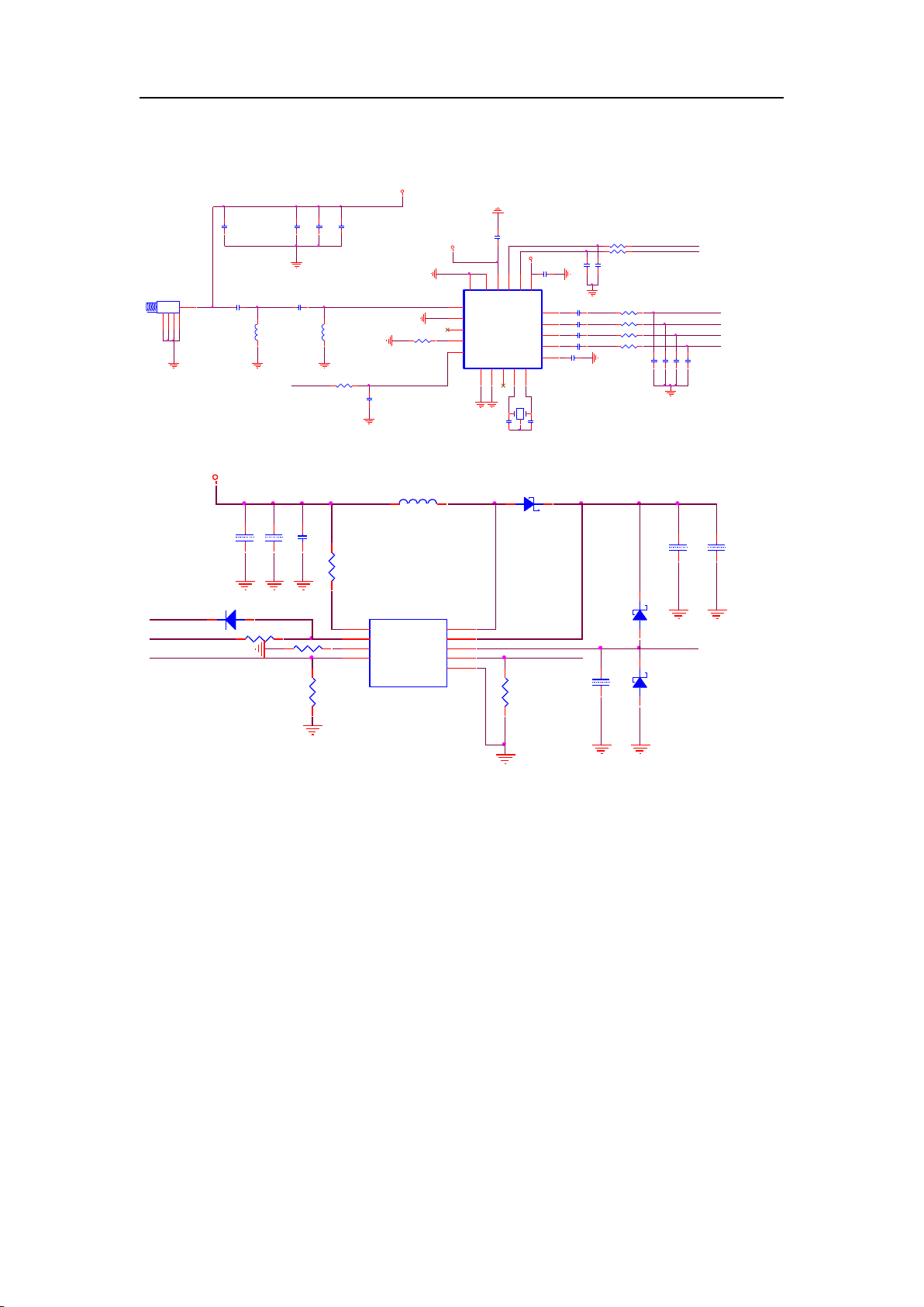
RDA5160 is a support global analog and digital terrestrial and cable tuning standard IC, generally
works as follows:
Digital and analog signal RF head (CNT1 is) passing through the filter capacitance and
inductance coupling, RDA5160 into the LNA (low noise amplifier) amplifies.
The SOC selected frequency (LO) via I2C control RDA5160, disposed IF bandwidth.
SOC control by controlling the amplitude of the IF AGC, and this point should be noted that:
AGC vary during the station search, the search platform will be completed at a fixed value, but this
time the amplitude of the intermediate frequency internal RDA5160 is adjustable.
RDA5160 internal block diagram as follows:
Input frequency range: 42 MHz-1002MHz
IF may be set 6MHZ, 7MHz, 8MHz
Built-in 1.8V LDO, to note that the built-in 1.8V output requires software to control output.
I2C can configure multiple addresses.
The main features of the chip are as follows:
Page 8
CV512H-U42 Service Manual
Line width=15mil
IF_QN
IF_QP
R303 51R
S2_S
C308
2.7pF/50V
S2_S
IF_IP
L16
5.6nH
S2_S
Trace1=32mm
LNB_POWERLNB_POWER_ET
RDA5815
QFN20
U27
RDA5815
S2_S
XOUT
8
VDD
11
XTAL2
9
BBIP
12
GND
20
VCC
16
BBQP
15
BBIN
13
AGC
5
XTAL1
10
PAD
21
VCC
19
GND
7
BBQN
14
LOOP
3
ADD
4
XOUT_EN
6
GND
2
RFIP
1
SDA
17
SCL
18
S2_3V3
C219 100nF/ 16V
S2_S
C242
27pF/50V
S2_S
IF_IN
C220 100nF/ 16V
S2_S
C285 100nF/ 16V
S2_S
L15
5.6nH
S2_S
C303
100pF/50V
S2_S
LNB_POWER
R190 100R
S2_S
R191 100R
S2_S
SCL_RF1
C299
2.2pF/50V
S2_S
SDA_RF1
LNB_PW_ET
C237
27pF/50V
S2_S
S2_3V3
R198 0R
S2_S
X2
27MHz/20PF/10PPM
S2_S
1 2
3
J18
RF_JAC K_THREAD
S2_S
1
234
5
close to Tuner pin
C213 100nF/ 16V
S2_S
C248 100nF/16V
S2_S
C22110pF/50V
S2_S
C306
1nF/50V
S2_S
C22210pF/50V
S2_S
C243
33pF/50V
S2_S
C22910pF/50V
S2_S
C23010pF/50V
S2_S
C307
1nF/50V
S2_S
C295
1nF/50V
S2_S
R288 1K
S2_S
RF_AGC
C302
2.2nF/50V
S2_S
C246
33pF/50V
S2_S
R304 51R
S2_S
C282
100pF/50V
S2_S
C214 100nF/ 16V
S2_S
R305 51R
S2_S
R306 51R
S2_S
U1
JW4005
S2_S or S2_ C
SW
1
VO
2
ISET
5
13/18V
7
FAULT
4
EN/EXTM
6
LDROP
8
LNB
3
GND
9
12VU
L1 6.8uH/ 1.8A
S2_S or S2_ C
R7
NC
NC
D9 SS14
S2_S or S2_ C
1
2
D4 SS14
S2_S or S2_ C
1 2
D11 SS14
S2_S or S2_ C
1
2
LNB_POWER
C6 10uF/16V
S2_S or S2_ C
C11 100nF/16V
S2_S or S2_ C
C5 10uF/16V
S2_S or S2_ C
FAULT
C13 10uF/ 25V
S2_S or S2_ C
C12 10uF/ 25V
S2_S or S2_ C
C14 1uF/25V
S2_S or S2_ C
R15
10K
S2_S or S2_ C
LNB-13/18V
R13 NC
NC
LNB-LDR OP
R12 200K
S2_S or S2_ C
DISEQC _OUT
R14
10K
S2_S or S2_ C
D10 4148
S2_S or S2_ C
2 1
LNB-EN
DVB- S2 (not used)
RDA5815 is a support for the global digital satellite signal tuning IC, the general work process is as
follows:
Digital and analog signals through the RF head (J2), after capacitive coupling filter, into the
RDA5815 LNA (low noise amplifier) to enlarge.
SOC through the I2C control RDA5815 frequency selection.
SOC through the AGC control control the amplitude of the frequency, which need to be
noted that: AGC in the search process will change, after the completion of the search station will
be fixed at a value, and this time the amplitude is RDA5815 internal adjustment.
RDA5 815 internal block diagram is as follows:
Page 9
CV512H-U42 Service Manual
12V供 电 ----2X8W
ZX1
SHORT
CA21 100nF/16V
CA7
NC/1nF/ 50V
NC
RA1
NC/10R
NC
AMP_ROUT+
RA48 NC/0RNC
靠近主IC端
RA3 NC/100K
CA19 220nF/16V
UA1
RDA3118e
SD
1
NC
13
PBTL14PVCC4
15
PVCC3
16
BSP1
17
OUTP1
18
PGND1
19
OUTP2
20
BSP2
21
BSN1
22
OUTN1
23
PGND2
24
FAULT
2
LINP
3
LINN
4
GAIN0
5
GAIN1
6
AVCC
7
AGND
8
GVDD
9
PLIMIT
10
RINN
11
RINP
12
OUTN2
25
BSN2
26
PVCC2
27
PVCC1
28
PAD
29
LA4 NC/22UH/ 1.11A
AMP_FILTER = '02'
CA17 220nF/16V
LA1 NC/22UH/ 1.11A
AMP_FILTER = '02'
CA4 220nF/ 16V
FBA4 FB1K/1.5A0
AMP_FILTER = '01'
CA12 220nF/16V
JA1
XH-4A-SPK_BTL
ROUT+
1
ROUT-
2
LOUT-
3
LOUT+
4
CA8 220nF/16V
FBA2 FB1K/1.5A0
AMP_FILTER = '01'
CA6
220nF/16V
CA22 1nF/50V
RA7 20K
LA3 NC/22UH/ 1.11A
AMP_FILTER = '02'
LA2 NC/ 22UH/1.11A
AMP_FILTER = '02'
CA13 1uF/16V
RA4 10R 1/10W
AOUT1R_G
CA3 1nF/50V
FBA3 FB1K/1.5A0
AMP_FILTER = '01'
FBA1 FB1K/1.5A0
AMP_FILTER = '01'
ZX2
SHORT
CA14 1uF/16V
CA10 1uF/16V
AOUT1L_G
RA8 10K
CA11 220nF/16V
CA18 220nF/16V
+12V_AMP
+12V_AMP
+12V_AMP
AOUT1R
红色圈起来的两组电容靠
近功放的距离基本相同
AOUT1L
AMP_LOUT+
TPA3120_SD
靠 PIN27,28放
网 络 AOUT1L和 AOUT1L_G必 须走差分
网 络 AOUT1R和 AOUT1R_G必 须走差分
CA1 100nF/16V
CA15
NC/1nF/ 50V
NC
RA6
NC/10R
NC
AMP_LOUT-
AMP_ROUT-
CA24 100nF/50V
CA23 100nF/50V
SPK_L
SPK_R
AOUT1RSPK_R
SPK_L
AOUT1L_G
AOUT1R_G
参数根据芯片方案而定,靠近主IC摆放
AOUT1L
TPA1
+12V_AMP
1
RA12 NC/10K
NC
DA1 0R
1 2
+
CA25 470uF/16V
12VU
+12V_AMP
CA5
3.3nF/50V
CA9
3.3nF/50V
CA16
3.3nF/50V
CA20
3.3nF/50V
AUDIO AMP
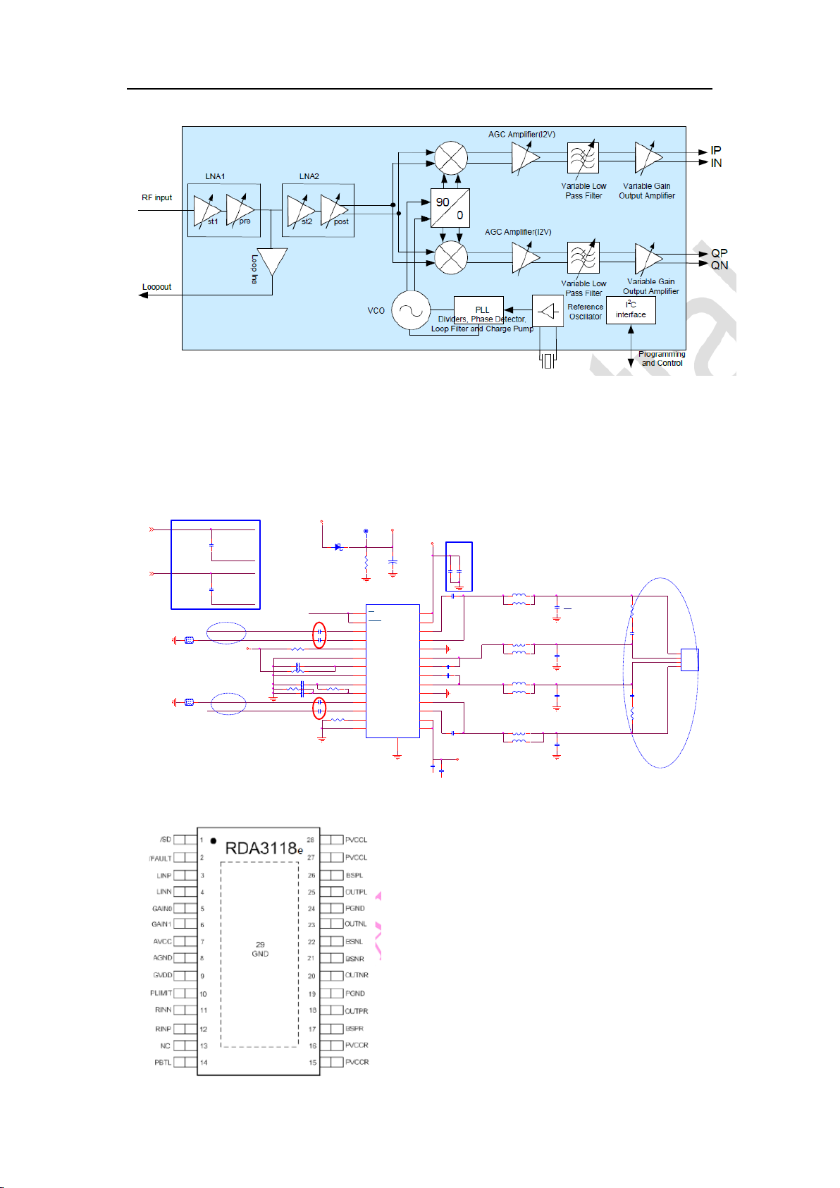
The main features of the chip are as follows:
Input frequency range: 250MHz-2150MHz
I2C can configure multiple addresses.
(g) Audio amplifier (AMP)
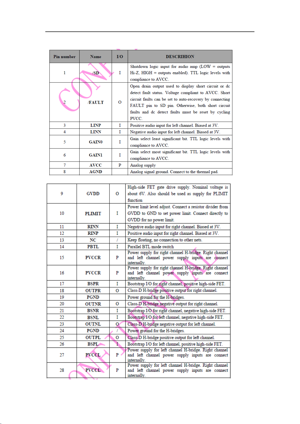
RDA3118e - a digital power amplifier chip, which PINs are defined as
follows:
Page 10
CV512H-U42 Service Manual
Each function pin is described as
follows:
Page 11
CV512H-U42 Service Manual
3.3VU
R5 10K
0
R6100K
0
PHONE OUT
Audio_L
Audio_R
GND
J2
PHONE JAC K_PJ-325
0
1
2
3
4
5
D2NCD1
NC
PHONE_L
PHONE_R
D3
NC
C3
22nF/25V
0
HP_L
HP_R
C2
22nF/25V
0
R2 100R
0
R1 100R
0
C4 10uF /6.3V
0
PHONE_L
C10 10uF/6. 3V
0
PHONE_R
R31K0R41K
0
CA2
100uF/16V
NC
D8
NC
1
2
D6
NC
1
2
5V_USB
USB0-D+
5V_USB
USB1_DM
USB0-D-
USB1_DP
USB1-D-
USB0_DM
D5
NC
1
2
D7
NC
1
2
USB0_DP
5VA
5V_USB
C20
10uF/6. 3V
0
USB0_DM <11>
USB0_DP <11>
C22
100nF/16V
0
GND
GND
GND
+5V
DM
DP
J5
USB-H
Singal USB
1
1
2
2
3
3
447
5
6
6
USB1_DM <11>
USB1_DP <11>
J3
PH-4A
Internal USB
1
2
3
4
J4
USB2.0-H _2A
NC
USB1_PWR
1
USB1_DM
2
USB1_DP
3
USB1_GND
4
USB0_PWR
5
USB0_DM
6
USB0_DP
7
USB0_GND
8
shield_GND
9
shield_GND
10
shield_GND
11
shield_GND
12
5V_USB
USB0-D-
USB1-D+
USB1-D-
USB0-D+USB1-D+
5V_USB
3.3VU
R10
10K
NC
L:ON
H:Standby
PowerON
5VU
5VA
UD6
TPS2065DDBVR
0
VOUT
1
GND
2
#FLG
3
EN
4
VIN
5
C7 1uF/ 6.3V
0
R8
10K
0
1V_EN
C15 10uF /6.3V
0
PowerON
1V_EN
C8
100nF/16V
0
R9
NC/ 0R
NC
FB3
FB120R/ 2A
NC
TP5
5VA
1
5V Switch Power
(H) EARPHONE
(I) USB
USB2.0 standard 500mA, the current limit is set to 1A; TPS2065DDBVR limiting 1A, with
overcurrent protection.
(J) MINI AV IN
Page 12
CV512H-U42 Service Manual
Audio_R
Audio_L
GND
CVBS
J8
MINI AV_PJ-320A
Mini AV
4
3
1
2
MINI AV Input
AV1_R_IN
AV1_L_IN
CVBS1_IN <11>
AIN2L
AIN2R
CVBS1_IN
AIN2R <11>
AIN2L <11>
AV1_IN
R64 150R
Mini AV
R65
75R
Mini AV
C74 220nF/16V
Mini AVC59
22nF/50V
Mini AV
C77
22nF/50V
Mini AV
C130
220pF/50V
Mini AV
C123
220pF/50V
Mini AV
R69 33K
Mini AV
R49 33K
Mini AV
PR
PB
GND
Y
J11
MINI YPBPR_PJ-320A
Mini YPBPR
4
3
1
2
R91
75R
Mini YPBPR or YPBPR2
R92
75R
Mini YPBPR or YPBPR2
Y_PB
Y_PR
R154 330R
Mini YPBPR or YPBPR2
Close IC
R160 150R
Mini YPBPR or YPBPR2
Y_I N
R86
75R
Mini YPBPR or YPBPR2
C191 47nF/25V
Mini YPBPR or YPBPR2
C190 47nF/25V
Mini YPBPR or YPBPR2
C109 47nF/25V
Mini YPBPR or YPBPR2
C110 47nF/25V
Mini YPBPR or YPBPR2
R93 150R
Mini YPBPR or YPBPR2
PR2_IN <11>
PR2_IN
R94 150R
Mini YPBPR or YPBPR2
PB2_IN <11>
PB2_IN
SOY2_I N
SOY2_I N <11>
YPbPr Input
Y2_I N <11>
Y2_I N
Y_IN
Y_PB
Y_PR
Y
GND
GND
GND
PB
PR
J7
AV3-8.4-5MF_Y PBPR
RCA Y PBPR
6
4
5
3
2
1
YPBPR
HS_VGA <11>
VS_VGA <11>
TXD0/VGA_SDA <11>
RXD0/VGA_SCL <11>
R296 1K
0
R298 1K
0
PC Analog Input
D54NCD56
NC
AIN1L
SCL_VGA2
SDA_VGA2
R291100R
0
R295100R
0
Close IC
R293
75R
0
R292
75R
0
R294
75R
0
AIN1R
Audio_L
Audio_R
GND
J20
PHONE J ACK_PJ-325
0
1
2
3
4
5
D61
NC
R
G
B
GND
GND
GND
GND
GND
GND
GND
SCL
SDA
H
V
NC
NC
NC
J22
VGA
0
1
6
2
7
3
8
4
9
5
11
12
13
14
15
10
16
17
R289 33K0
R280 33K
0
D47NCD53
NC
D58
NC
PC Audio Input
D60NCD59
NC
D62NCD57
NC
R301
10K
0
D55
NC
R300
10K
0
R286150R
0
R282
4K7
0
R283
4K7
0
5VU
C292
33pF/50V
NC
C293
33pF/50V
NC
PC DDC
R285150R
0
RXD0/VGA_SCL
R284150R
0
C296
22pF/50V
NC
R_IN
R_IN <11>
C297
22pF/50V
NC
G_IN <11>
G_IN
VS_VGA
HS_VGA
TXD
C195 47nF /25V
0
C194 47nF /25V
0
C193 47nF /25V
0
B_IN <11>
B_IN
RXD
AIN1L <11>
AIN1R <11>
SCL_VGA2
SDA_VGA2
R299 100R
0
R297 100R
0
RXD
TXD
(K) Ypbpr IN (compatible with RCA YPbPr2)
(L) VGA +Audio IN (for external Debug)
(M) SCART (compatible RCA AV1, RCA AV OUT)
Page 13
CV512H-U42 Service Manual
C245
22nF/25V
SCART&AV-OUT
AU_RIN
GNDB
GNDVI
AIL
BIN
VOUT
FunSel
VIN
GNDG
SHILED
N.C.
GIN
N.C.
GNDR
RIN
AOR
AIR
RGBSW
AOL
GNDSW
GNDA
GNDVO
CN2
SCART-104B
SCART
1
2
3
4
5
6
7
8
9
10
11
12
13
14
15
16
17
18
19
20
21
AU_LIN
R259
75R
SCART
R260
75R
SCART
D45
NC
LINEOUT_L <11>
LINEOUT_L
LINEOUT_R
LINEOUT_R <11>
D36
NC
SC1_VIN
SC1_RIN
C271
470nF/10V D VD/0R N ODVD
DVD(470nF)/ SCART(0R)
C273
470nF/10V D VD/0R N ODVD
DVD(470nF)/ SCART(0R)
Y1_IN _D
PR1_IN_D
PB1_IN_D
C272
470nF/10V D VD/0R N ODVD
DVD(470nF)/ SCART(0R)
SC1_AU_LIN
R268
75R
SCART&AV1
D41
NC
CVBS0_IN <11>
CVBS0_IN
D40
NC
Close IC
R273 33K
SCART&AV1
SCART_SOG
SC1_FS SC ART1_FUNSEL
SC1_BIN
SC1_GIN
SC1_RIN
SC1_AU_ROU T
R155 150R
SCART&AV1
SC1_FB FSCART_FB
SC1_VIN
SC1_AU_LOUT
C234 47nF/25V
SCART
R256 33K
SCART&AV1
C192 220nF/16V
SCART&AV1
D44
NC
R248 330R
SCART&AV-OUT
D42NCD43
NC
C277 1uF/ 16V
SCART&AV-OUT
SCART1 Input
C276 1uF/ 16V
SCART&AV-OUT
SC1_BIN
R247 330R
SCART&AV-OUT
D38
NC
GND_HSAD C
SC1_AU_LOUT
SC1_AU_ROU T
SC1_GIN
R187 150R
SCART
SC1_AU_RI N
SC1_VOUT CVBS_OUT
D46
NC
C240
22nF/25V
SCART&AV-OUT
R261
75R
SCART
R220
75R
SCART&AV-OUT
D12
NC
CVBS_OUT
CVBSO
<11>
CVBSO
CVBS Output
SCART FUNCTION SEL
R250
75R
Scart
SCART FAST BLANKING
R99
6K8
Scart
SCART_FB
SCART_FS
SCART_FB
SCART_FS <11>
SCART_FB <11>
NOTE:0~2V ->0~ 0.314V (TV MODE)
5~8V ->0.785~1.255V (16:9 AV MODE)
8.8~12V ->1.38~1.883V(4:3 AV MODE)
SCART_FS
C107
100pF/50V
Scart
D37
NC
D35
NC
C102
NC/ 100pF/50V
NC
FSCAR T_FB
SCART1_FU NSEL
0-0.4V CVBS
1-3V RGB
Scart Function switch
R100 220R
Scart
R251 22K
Scart
R171
4K7
NC
DVD & S805
R212
10K
DVD
C210
22pF/50V
DVD
DVD_STB
R164
10K
NC
3.3VA
R177
4K7
DVD
C228
100nF/16V
DVD
12VA
5V_DVD
C212
100nF/16V
DVD
DVD_IR
DVD_AUTO
R172 100R
DVD
R174 100R
DVD
J15
PH-8A_DVD POWER
DVD
DVD_STB
1
DVD_AUTO
2
DVD_IR
3
+12V
4
GND
5
GND1
6
+5V
7
+5V1
8
DVD_ON/ OFF
R169 100R
DVD
C203
100nF/16V
DVD or S805
R158 200K
DVD or S805
R163 10K
DVD or S805
12VU
Q10
3904
DVD or S805
1
2
3
12VA
R146
47K
DVD or S805
Q11 GV3407
DVD or S805
3
1
2
C208
100nF/16V
DVD
C206
100nF/16V
DVD
R176
4K7
NC
Q4
3407
DVD
3
1
2
TP7
5V_DVD
1
5VU 5V_DVD
TP8
12VA
1
(N) DVD features
Page 14

CV512H-U42 Service Manual
R221
75R
Internal Y PBPR
R222
75R
Internal Y PBPR
R223
75R
Internal Y PBPR
DVD_PbinDVD_Pb
DVD_Pr
DVD_Y DVD_Yin
C225
470nF/10V
Internal Y PBPR
C218
470nF/10V
Internal Y PBPR
DVD_Prin
C207
470nF/10V
Internal Y PBPR
DVD_LIN
DVD_RIN
R249 33K
Internal Y PBPR
R218 33K
Internal Y PBPR
J16
PH-11A_Y PBPR&AUDIO
Internal Y PBPR
GND
1
Y
2
GND1
3
Pr
4
GND2
5
Pb
6
LIN
7
GND3
8
RIN
9
GND4
10
SPDIF
11
MHL
HPD_HD MI_B_2
RXM0_B
R215
1M
0
SCL_HDMI_B
SDA_HDMI_B
RXCM_B
R266 0R
D48NC
RXCP_B
D34NC
RXCM_B <11>
RXCM_B
RXM1_B
RXP0_B
RXM2_B <11>
RXP2_B <11>
RXM0_B
RXM2_B
HPD_HD MI_B
RXP1_B
RXCP_B
RXP2_B
RXM1_B <11>
RXP1_B <11>
SDA_HDMI_B
SCL_HDMI_B
SCL_HDMI_B <11>
SDA_HDMI_B <11>
HPD_HD MI_B <11>
RXP0_B <11>
RXCP_B <11>
RXM0_B <11>
MHL_DET
RXP0_B
C268
39pF/50V
R214 68R
0
R193 68R
0
RXM1_B
HPD_HD MI_B_2
5V_MHL
HPD_HD MI_B
RXP1_B
RXM2_B
R216
4K7
0
CON2
HDMI
DATA2+
1
DATA2_SHIELD
2
DATA2-
3
DATA1+
4
DATA1_SHIELD
5
DAT1A-
6
DATA0+
7
DATA0_SHIELD
8
DATA0-
9
CLK+
10
CLK_SHIELD
11
CLK-
12
CEC
13
NC
14
SCL
15
SDA
16
CEC_GND
17
+5V POWER
18
HOT PLUG
19
20
20
21
21
23
23
22
22
CEC_B
RXP2_B
HDMI PORT-B
D25NC
5VU
D27NC
R194
47K
0
Close IC
(K) HDMI signal
Through the menu to select the way you want to play the signal path to the main
core U 7 (S2C512), the master chip U 7 (S2C512), receives the signal image scaling, and outputs
the OSD superimposing LVDS signal for driving the liquid crystal panel; HDMI1 with ARC,
HDMI 2 MHL-compatible functions
Page 15

CV512H-U42 Service Manual
CON1
HDMI
DATA2+
1
DATA2_SHIELD
2
DATA2-
3
DATA1+
4
DATA1_SHIELD
5
DAT1A-
6
DATA0+
7
DATA0_SHIELD
8
DATA0-
9
CLK+
10
CLK_SHIELD
11
CLK-
12
CEC
13
NC
14
SCL
15
SDA
16
CEC_GND
17
+5V POWER
18
HOT PLUG
19
20
20
21
21
23
23
22
22
RXM1_C
C37
39pF/50V
0
HPD_HD MI_CHPD_HD MI_C_2
CEC_C
V_5V_HDMI_VBUS_C
HDMI PORT-C
RXP0_C
D20NC
D22NC
RXCP_C
RXM0_C
RXP2_C
RXCM_C
R147
4K7
0
R162 68R
0
R137
47K
0
RXM1_C
RXP0_C
RXP2_C <11>
RXCM_C <11>
RXCM_C
RXM2_C <11>
RXCP_C
RXP2_C
RXM0_C
RXM2_C
RXP1_C <11>
SDA_HDMI_C
SCL_HDMI_C
HPD_HD MI_C
RXP1_C
HPD_HD MI_C <11>
RXP0_C <11>
RXM1_C <11>
RXM0_C <11>
SCL_HDMI_C <11>
SDA_HDMI_C <11>
RXCP_C <11>
R144
1M
0
RXP1_C
RXM2_C
D23NC
D24NC
SCL_HDMI_C
SDA_HDMI_C
HPD_HD MI2_C
R131 68R
0
R143 68R
0
HPD_HD MI_C_2
R240
4K7
ARC
HDMI ARC
HDMI_ARC <11>
HDMI_ARC
R239
10K
ARC
ARC
R207
82R
ARC
HDMI_ARC
C259 1uF/10V
ARC
R197
180R
ARC
V_5V_HDMI_A
ARC_DET
ARC_DET <11>
ARC_DET
HDMI CEC
R110 68R
CEC
R111
27K
CEC
D16
4148
CEC
2
1
CEC_HD MI
CEC_HD MI <11>
CEC_B
3.3VU
CEC_A
CEC_C
CEC_HD MI
R180
0R
300K MHL/0R HDMI
MHL 充 电
1A
CD_SEN SE <11>
CD_SEN SE
HDMI MHL
5V_MHL
C39 10uF /6.3V
MHL
R19
10K
MHL
R15 10K
MHL
ENVBUS
U2 SGM2588
MHL
OUT
1
GND
2
OC
3
EN(EN)
4
IN
5
C38 10uF/ 6.3V
MHL
5VU
MHL_DET CD_SEN SE
R181 33R
MHL
ENVBUS
ENVBUS <11>
C215
47nF/25V
MHL
4. FAQ (TroubleShooting)
:
(1) three non- black (no light, no image, no sound):
Page 16

CV512H-U42 Service Manual
5. Upgrade process
USB upgrade:
(1) The extension of software file is *.bin, it is copied to the root directory;
(2) USB disk connected to the USB port on the TV, the power to open automatically upgrade;
Page 17

CV512H-U42
Common problems solution
—Power Unit Problem Solving
—Display Unit Problem Solving
—Audio Unit Problem Solving
—Functional Unit Problem Solving
Page 18

ANTENNA
S2T512
DVB-T2/T/C/S2
RGB
4 M Byte
HDMI2 WITH MHL
SPDIF
CVBS2
Dual LVDS 10BIT
VGA(PC)
IR/KEYPAD
INTERFACE
R/L Audio
YPBPR*2
CI_CARD
USB*2
USB 2.0*2
CODE FLASH
TS X8
I2C
1920x1080
RDA3118e
LINE_OUT
AV1&2
PANEL
H/VSYNC
CATS X8
CI_ADD X12
CI_DATA X8
LINE_OUT
RDA5160
EARPHONE
YPBPR1
CVBS1
HDMI*3
HP_L/R
LINE_IN x 3
HDMI1 WITH ARC
IF/IQ
DVD R/L
SCART R/L
PC R/L
AV1 R/L
DIO1717
CVBSOUT
CVBSOUT
DVD YPbPr
Scart RGB
SGM331
SPDIFHDMI3
RDA5815M
IF_IN/IF_IP/IF_QN/IF_QP
Page 19

Picture 1: Power Units Problem Solving
(Mainboard can not boot)
N
In stand-by condition,
Check pin 5,6 of TPI1,
Whether got 12V?
Y
Check AC power
supply circuit
N
Check the UD1,
UD5 related
devices
Whether main board testing point TP1 got 5V?
testing TP4 got 3.3v?
Y
Normal booting
After power on, check
whether testing point TP2
got 3.3v testing point TP9
got 1.5v,testing TP6 got 1.2v?
YN
Whether power chip
(UD3,UD4,UD2) works?
OK
Page 20

Picture 2
Display unit ( black screen)
Black screen
Whether the voltage that
power panel supply to Inverter
is normal?
Y
Check the socket that controls Inverter,
whether the voltage output from pin 4 of TPI1
N
N Y
Check and repair the
network that controls
Inverter ON/OFF
is in high level?
Check the external power supply circuit
Inverter is broken or
connecting line is not good
Page 21

N
No sound
Picture 3
If there is any audio signal input
Audio part (no sound)
or Whether amplifier power supply
is normal?
Y
Whether the volume,
MUTE
Y
setting is normal?
YN
Whether there is
signal output from JA1?
N
Whether there is signal
Y
input in
UA1RDA3118epin 3/12 ?
N
Check
peripheral
audio
equipment:
amplifier
power
supply
Resetting
Check
external
loudspeaker
Check and repair
network
of the connecting
part between
U7 and UA1
Check if the U7 welded
Well , re-weld UA1 or change
RDA3118e chip.
circuit
Page 22

TV no searching
/no image
Check whether
external RF input signal
Picture 4
T2+T+C Function unit (ATV/DTV video
N
is normal?
broke down)
Y
Whether main board testing TP13 output 3.3V?
Y
whether there is I2C data?
Y
Check Tuner have single output?
Y
N
Check R302,R308,
N
N
Check and
repair
peripheral
RF
Repair UT1 to U7
middle-
Frequency part
net,
Check the
tuner UT1
related circuits
Check and
repair UD3
Check and repair
network
I2C network
equipment
Page 23

TV no searching
/no image
Check whether
external RF input signal
Picture 5
S2 Function unit (DTV video broke
N
is normal?
down)
Y
Whether main board testing FB14 output 3.3V?
Y
whether there is I2C data?
Y
Check Tuner have single output?
Y
N
Check R190,R191,
N
N
Check and
repair
peripheral
RF
Repair U27 to U7
middle-
Frequency part
net,
Check the
tuner U27
related circuits
Check and
repair UD3
Check and repair
network
I2C network
equipment
Page 24

TV no sound, only picture
Whether there is
sound under PC AV?
Picture 6
Function unit (ATV/DTV no
sound)
N
Y
Whether software is
OK? input system is
set correctly?
Y
Refer to “NO SOUND”
repair guide
Change U7
Page 25

Picture 7
Under PC
Function unit
PC
Image not
in the middle
Miss color,
Color
cast
Whether U7
R.G.B input signal is normal?
Whether the
contact of
VGA socket
is good?
Image
shakes
Whether VS,HS signal
is regular or stable?
No signal
Whether the
contact of
Carry out
auto-adjust
operation
Y N
The system
setting
is incorrect,
Check VGA
input circuit
Y N
OSD setting
doesn’t match,
reset it,
Check VS.HS
circuit
VGA socket
is good?
Check VS.HS
circuit
reset it
or input mode
doesn’t support
Page 26

Picture 8
Function unit
HDMI
Under HDMI
No image
Check whether
HOTPLUG pin is
high?
Whether HDMI
contact
is good?
There is image
but no sound
Whether there is
Y
Y
Check HDMI related
network of U7
N
Y
sound under PC?
N
Change the software and
Re-weld the U7&HDMI
connecter
Check HDMI
and input
network
Check HDMI
input network
and EDID
Refer to "no
sound" repair
guide
Page 27

Picture 9
Function unit
MHL
Under HDMI
Y
No image
There is image
but no sound
Whether HDMI
N
contact
is good?
Testing the
C21 whether
have 5V
Y
Check whether the network
Re-plug the
Refer to "no
HDMI cable
sound" repair
guide
N
between the CON2 &U7 is
Ok?
Y
Re-solder
the CON2&U7
or change the
N
Repair the
network
Check whether the
software is correct
Y
Re-solder the U2
or change the U2
N
Change software
CON2&U7
Page 28

5
4
3
2
1
+5V_Standby POWER 3A
RD2 100K
CD17
NC/100nF/16V
5
4
0
0
0
CD1 100nF/16V
6
VBST
3
VIN
5
NC
RD3 NC/18K
UD2
TLV62569
IN4SW
EN1FB
2
RD7
NC/51K
SW
VFB4EN
GND
1
UD1
TPS563201
3
5
GND
TP4
3.3VU
3.3VU
1
C18 100nF/16V
C17 10uF/6.3V
12VU
D D
+12V
CD9 100nF/16V
CD8 10uF/16V
Vout=0.768*(1+R1/R2)
1V System Power 2A
C C
5VU
1V_EN
RD5 10K
CD11 100nF/16V
CD10 10uF/6.3V
Vout= 0.6*(1+R1/R2)
改用
8528芯片:Vout=Vout=0.6x(1+(13K/12K))=1.25V
B B
3.3V STANDBY POWER
5VU
A A
UD5
LP3992-33B5F
VIN1VOUT
EN3ADJ
C16
100nF/16V
GND
2
5
TP1
5VU
LD1
4.7uH/6A
2
1
RD1
R1
68K_1%
CD6 10uF/6.3V
CD4 10uF/6.3V
CD2 10uF/6.3V
CD5 100nF/16V
CD3 10uF/6.3V
RD4
R2
12K_1%
3A
CD12 10uF/6.3V
CD27 100nF/16V
CD15 NC/1uF/6.3V
CD13 10uF/6.3V
CD14 100nF/16V
2A
0
NOTE:DDR
4
V_1V
CD16 NC/1uF/6.3V
UD4
LP3983SAB5F-08
VIN1VOUT
EN3ADJ
电压调高到
TP6
V_1V
LD2 2.2uH/2.2A
1
R1
RD6
13K_1%
R2
RD8
12K_1%
1.5V DDR Power
3.3VA
Vout= 0.8*(1+R1/R2)=1.537V
2
GND
FB120R/3A
NC
5
4
1.53V
5VU
FB2
1.5VA
TP9
1.5VA
CD29
0
CD25 10uF/6.3V
CD26 100nF/16V
1
22pF/50V
47K_1%
RD16
R1
RD15
51K_1%
R2
0
0
5V Switch Power
PowerON
PowerON
L:ON
H:Standby
3.3V System Power
5VU
3VA_EN
CD19 100nF/16V
CD18 10uF/6.3V
Vout=0.6*(1+R1/R2)=0.6*(1+100K/22K)=3.33V
M4
M3
1
1
orientpad
orientpad
M1
M2
1
1
orientpad
orientpad
MARK
12VU
JAGE1
1
1
2
2
PH-2A
<FUNCTION>
3
3.3VU
NC
RD9 100K
RD11 NC/51K
A7
1
AHOLE138
R10
10K
1V_EN
UD3
BL8026+TLV62565+SY8088
IN4SW
EN1FB
2
1
GND
5VU
C7 1uF/6.3V
A2
AHOLE138
1V_EN
LD3 6.8uH/1.8A
3
5
1
2
R1
R2
A3
AHOLE138
TP5
UD6
TPS2065DDBVR
5
VOUT
VIN
GND
4
#FLG3EN
10K
1
R8
RD10
RD12
A6
AHOLE138
0
0
0
0
0
TP2
3.3VA
1
100K_1%
CD28NC/10uF/6.3V
CD21 10uF/6.3V
CD20 10uF/6.3V
NC
22K_1%
1A
A5
AHOLE138
AHOLE138
1
1
Size Document Number Rev
Size Document Number Rev
Size Document Number Rev
A3
A3
A3
Date: Sheet
Date: Sheet
Date: Sheet
5VA
1
1
2
CD22 100nF/16V
A8
NC/0R
R9
NC
CD23 NC/1uF/6.3V
1
3VA_EN
3.3VA
CD24 NC/1uF/6.3V
A9
AHOLE138
C15 10uF/6.3V
3VA_EN
A10
AHOLE138
1
Power Supply
Power Supply
Power Supply
C8
100nF/16V
Title
Title
Title
5VA
FB3
FB120R/2A
NC
CV512H-U42
CV512H-U42
CV512H-U42
316Friday, June 02, 2017
316Friday, June 02, 2017
316Friday, June 02, 2017
1
11
11
11
of
of
of
Page 29

5
4
3
2
1
HPD_HDMI_A_2
0
0
0
0
0
SDA_HDMI_A
R276 68R
SCL_HDMI_A
R279 68R
HPD_HDMI_A_2 HPD_HDMI_A
R208 68R
MHL
0
0
0
SDA_HDMI_B
R214 68R
SCL_HDMI_B
R193 68R
0
0
HPD_HDMI_B_2 HPD_HDMI_B
HPD_HDMI_C_2
0
0
0
SDA_HDMI_C
R143 68R
SCL_HDMI_C
R131 68R
0
0
HPD_HDMI_C_2 HPD_HDMI_C
R166 68R
4
0
R266 0R
0
HPD_HDMI_A
SDA_HDMI_A
SCL_HDMI_A
HPD_HDMI_B
SDA_HDMI_B
SCL_HDMI_B
RXP2_B
RXM2_B
RXP1_B
RXM1_B
RXP0_B
RXM0_B
RXCP_B
RXCM_B
0
HPD_HDMI_C
SDA_HDMI_C
SCL_HDMI_C
RXP2_C
RXM2_C
RXP1_C
RXM1_C
RXP0_C
RXM0_C
RXCP_C
RXCM_C
C289
39pF/50V
RXP2_A
RXM2_A
RXP1_A
RXM1_A
RXP0_A
RXM0_A
RXCP_A
RXCM_A
C287
39pF/50V
0
C268
39pF/50V
Close IC
0
HPD_HDMI_A <11>
SDA_HDMI_A <11>
SCL_HDMI_A <11>
RXP2_A <11>
RXM2_A <11>
RXP1_A <11>
RXM1_A <11>
RXP0_A <11>
RXM0_A <11>
RXCP_A <11>
RXCM_A <11>
HPD_HDMI_B <11>
SDA_HDMI_B <11>
SCL_HDMI_B <11>
RXP2_B <11>
RXM2_B <11>
RXP1_B <11>
RXM1_B <11>
RXP0_B <11>
RXM0_B <11>
RXCP_B <11>
RXCM_B <11>
0
HPD_HDMI_C <11>
SDA_HDMI_C <11>
SCL_HDMI_C <11>
RXP2_C <11>
RXM2_C <11>
RXP1_C <11>
RXM1_C <11>
RXP0_C <11>
RXM0_C <11>
RXCP_C <11>
RXCM_C <11>
3
HDMI ARC
V_5V_HDMI_A
R240
4K7
R239
10K
HDMI MHL
MHL_DET
300K MHL/0R HDMI
ENVBUS
HDMI CEC
V_5V_HDMI_VBUS_C
ARC_DET
CEC_A
CEC_B
CEC_C
RXP2_C
RXP1_C
RXP0_C
RXCP_C
SCL_HDMI_C
CEC_C
SCL_M
<13,15,16>
ARC
ARC
R180
300K
5VU
C9 10uF/6.3V
R17
10K
MHL
MHL
MHL
MHL
MHL
3.3VU
5
4
R111
27K
D16
4148
2 1
11
13
15
17
19
R16 10K
J14
HDMI_ARC
ARC_DET
ARC
C259 1uF/6.3V
ARC
ARC
ARC
CD_SENSE
R181 33R 0
C215
47nF/25V
MHL
IN
U2 SGM2588
R110 68R
TMDS Data2+1TMDS Data2TMDS Data1+3TMDS Data1TMDS Data0+5TMDS Data0TMDS Clock+7TMDS ClockHDMI_SCL9HDMI_SDA
GND
HDMI+5V
GND2
CEC
SCL
HEADER 2x10_HDMI Internal HDMI
OUT
GND
OC3EN(EN)
1
2
CEC or ARC
CEC or ARC
CEC or ARC
2
5V_MHL
CEC_HDMI
GND1
HPD
GND3
SDA
1A
C21 10uF/6.3V
+5V
2
4
6
8
10
12
14
16
18
20
HDMI_ARC <11>
ARC_DET <11>
R197
HDMI_ARC
180R
R207
82R
ENVBUS
ENVBUS <11>
CD_SENSE
CD_SENSE <11>
MHL
充电
CEC_HDMI
CEC_HDMI <11>
RXM2_C
RXM1_C
RXM0_C
RXCM_C
SDA_HDMI_C
HPD_HDMI_C
5VA
SDA_M <13,15,16>
Title
Title
Title
CV512H-U42
CV512H-U42
CV512H-U42
Size Document Number Rev
Size Document Number Rev
Size Document Number Rev
Custom
Custom
Custom
Date: Sheet
Date: Sheet
Date: Sheet
HDMI
HDMI
HDMI
of
of
of
416Friday, June 02, 2017
416Friday, June 02, 2017
416Friday, June 02, 2017
1
11
11
11
CLK+
SDA
SCL
CEC
CLK-
CLK+
HPD_HDMI2_A
V_5V_HDMI_A
D39NC
ARC
19
18
17
16
15
14
NC
13
12
11
10
9
8
7
6
5
4
3
2
1
19
18
17
16
SDA
15
SCL
14
NC
13
CEC
12
CLK-
11
10
9
8
7
6
5
4
3
2
1
R272
4K7
D50NC
D51NC
D33NC
D26NC
HPD_HDMI2_B HPD_HDMI_B_2
5V_MHL
D34NC
R216
D27NC
D48NC
D25NC
R278
R277
1M
47K
ARC
CEC_A
RXCM_A
RXCP_A
RXM0_A
RXP0_A
RXM1_A
RXP1_A
RXM2_A
RXP2_A
5VU
R215
R194
1M
47K
4K7
CEC_B
RXCM_B
RXCP_B
RXM0_B
RXP0_B
RXM1_B
RXP1_B
RXM2_B
MHL_DET
RXP2_B
HDMI PORT-A
HDMI
20
HOT PLUG
20
+5V POWER
CEC_GND
23
D D
23
CLK_SHIELD
DATA0-
DATA0_SHIELD
22
DATA0+
22
DAT1A-
DATA1_SHIELD
DATA1+
DATA2-
DATA2_SHIELD
21
DATA2+
21
CON3
0
HDMI PORT-B
C C
HDMI
20
HOT PLUG
20
+5V POWER
CEC_GND
23
23
CLK_SHIELD
DATA0-
DATA0_SHIELD
22
DATA0+
22
DAT1A-
DATA1_SHIELD
DATA1+
DATA2-
DATA2_SHIELD
21
DATA2+
21
CON2
0
B B
HDMI PORT-C
HPD_HDMI2_C
V_5V_HDMI_VBUS_C
D24NC
HDMI
20
23
22
21
A A
CON1
NO Internal HDMI
HOT PLUG
20
+5V POWER
CEC_GND
23
CLK_SHIELD
DATA0-
DATA0_SHIELD
DATA0+
22
DAT1A-
DATA1_SHIELD
DATA1+
DATA2-
DATA2_SHIELD
DATA2+
21
CLKCLK+
19
18
17
16
SDA
15
SCL
14
NC
13
CEC
12
11
10
9
8
7
6
5
4
3
2
1
D23NC
D22NC
D20NC
5
R144
R147
R137
1M
4K7
47K
CEC_C
RXCM_C
RXCP_C
RXM0_C
RXP0_C
RXM1_C
RXP1_C
RXM2_C
RXP2_C
Page 30

5
4
3
2
1
PC Analog Input
1617
GND
J22
D57
R
1
GND
6
G
2
GND
7
B
3
GND
8
NC
4
NC
9
GND
5
GND
10
D55
NC
R300
10K
TXD
SCL_VGA2
SDA_VGA2
R291100R
R295100R
0
0
10K
0
0
D58
NC
D59
NC
VS_VGA
HS_VGA
D60
R293
R292
NC
75R
75R 0
NC
NCR301
C296
C297
22pF/50V
22pF/50V
R294
75R
VS_VGA <11>
HS_VGA <11>
R286150R
R285150R
R284150R
0
0
0
0
0
RXD
TXD
D54
NC
D56
NC
Close IC
SCL_VGA2
SDA_VGA2
C195 47nF/25V
C194 47nF/25V
C193 47nF/25V
0
0
0
R296 1K
R298 1K
0
0
R297 100R
R299 100R
0
0
R_IN
G_IN
B_IN
R_IN <11>
G_IN <11>
B_IN <11>
5VU
R282
R283
4K7
4K7
RXD0/VGA_SCL
C292
C293
33pF/50V
33pF/50V
PC DDC
0
0
NC
NC
RXD0/VGA_SCL <11>
TXD0/VGA_SDA <11>
NC
11
RXD
SDA
D D
C C
12
H
13
V
14
SCL
15
VGA
GND
0
D61
D62
NC
NC
NC
PC Audio Input
J20
GND
1
Audio_R
3
5
4
2
Audio_L
PHONE JACK_PJ-325
0
B B
D47
NC
R280 33K
R289 33K0
D53
NC
0
AIN1R
AIN1L
AIN1R <11>
AIN1L <11>
Dual USB Input
6
5
Singal USB
6
USB-H
5V_USB
C22
J5
1
1
2
2
3
3
447
100nF/16V
+5V
DM
DP
GND
3
C20
10uF/6.3V
5V_USB
NC
CA2
100uF/16V
USB0-D-
USB0-D+
5VA
0
0
Title
Title
Title
CV512H-U42
CV512H-U42
CV512H-U42
Size Document Number Rev
Size Document Number Rev
Size Document Number Rev
Custom
Custom
Custom
Date: Sheet
Date: Sheet
Date: Sheet
2
PC & USB
PC & USB
PC & USB
516Friday, June 02, 2017
516Friday, June 02, 2017
516Friday, June 02, 2017
1
11
11
11
of
of
of
5V_USB
J3
PH-4A
USB0_DM
USB0_DP
USB1_DM
USB1_DP
5V_USB
4
3
2
1
4
USB1-DUSB1-D+
USB0_DM <11>
USB0_DP <11>
USB1_DM <11>
USB1_DP <11>
GND
GND
J4
USB1_PWR
USB1_DM
USB1_DP
USB1_GND
USB0_PWR
USB0_DM
USB0_DP
USB0_GND
A A
shield_GND
shield_GND
shield_GND
shield_GND
USB2.0-H_2A
NC
1
2
3
4
5
6
7
8
9
10
11
12
5V_USB
5
USB0-DUSB0-D+
USB1-DUSB1-D+
D8
D6
1 2
1 2
NC
NC
D7
D5
1 2
1 2
NC
NC
Internal USB
Page 31

5
4
3
2
1
YPbPr Input
Y
4
PB
3
PR
2
GND
CVBS
Audio_L
Audio_R
GND
1
4
3
2
1
D D
J11
MINI YPBPR_PJ-320A
Mini YPBPR
C C
MINI AV Input
J8
MINI AV_PJ-320A
Mini AV
B B
Y_IN
Y_PB
Y_PR PR2_IN
R86
R92
R91
75R Mini YPBPR or YPBPR2
75R
75R
AV1_IN CVBS1_IN
R64 150R
AV1_R_IN
R49 33K
AV1_L_IN
R69 33K
C77
22nF/50V
C59
22nF/50V
R65
75R
Mini AV
Mini AV
Mini AV
Mini AV
Mini AV
Mini AV
Mini AV
R160 150R
R154 330R
R93 150R
R94 150R
Mini YPBPR or YPBPR2
Mini YPBPR or YPBPR2
C74 220nF/16V
C130
C123
220pF/50V
Mini AV
Mini AV
220pF/50V
Close IC
C191 47nF/25V
C190 47nF/25V
C109 47nF/25V
C110 47nF/25V
AIN2R
AIN2L
Y2_IN
SOY2_IN
PB2_IN
Mini YPBPR or YPBPR2
Mini YPBPR or YPBPR2
Mini YPBPR or YPBPR2
Mini YPBPR or YPBPR2
Mini YPBPR or YPBPR2
Mini YPBPR or YPBPR2
Mini YPBPR or YPBPR2
Mini YPBPR or YPBPR2
CVBS1_IN <11>
AIN2R <11>
AIN2L <11>
Y2_IN <11>
SOY2_IN <11>
PB2_IN <11>
PR2_IN <11>
YPBPR
J7
AV3-8.4-5MF_YPBPR
Y
2
GND
1
PB
A A
4
3
6
5
RCA YPBPR
GND
PR
GND
5
4
Y_PB
Y_PR
Y_IN
Title
Title
Title
CV512H-U42
CV512H-U42
CV512H-U42
Size Document Number Rev
Size Document Number Rev
Size Document Number Rev
A
A
A
Date: Sheet
Date: Sheet
3
Date: Sheet
2
YPbPr & AV
YPbPr & AV
YPbPr & AV
616Friday, June 02, 2017
616Friday, June 02, 2017
616Friday, June 02, 2017
of
of
of
1
11
11
11
Page 32

5
SCART1 Input
CN2
21
SHILED
VOUT
GNDVO
D D
RIN
GNDR
GIN
GNDG
BIN
GNDB
AOL
AOR
SCART-104B
SCART
C C
SC1_VIN
20
VIN
SC1_VOUT CVBS_OUT
19
18
GNDVI
17
SC1_FB FSCART_FB
16
RGBSW
SC1_RIN
15
14
GNDSW
13
12
N.C.
SC1_GIN
11
10
N.C.
9
SC1_FS SCART1_FUNSEL
8
FunSel
SC1_BIN
7
AU_LIN
6
AIL
5
4
GNDA
SC1_AU_LOUT
3
AU_RIN
2
AIR
SC1_AU_ROUT
1
GND_HSADC
D45
NC
SC1_AU_LIN
R256 33K
SC1_AU_RIN
R273 33K
SCART&AV1
SCART&AV1
D46
D38
NC
NC
SC1_VIN
D36
SC1_AU_LOUT
SC1_AU_ROUT
SC1_GIN
SC1_BIN
SC1_RIN
D44
D42
NC
NC
D41
NC
4
C192 220nF/16V
C234 47nF/25V
Close IC
C277 1uF/16V
C276 1uF/16V
C245
22nF/25V
22nF/25V
R261
75R
R259
75R
SCART&AV1
SCART
SCART&AV-OUT
SCART&AV-OUT
SCART&AV-OUT
SCART&AV-OUT
SCART&AV-OUT
SCART&AV-OUT
R260
75R
CVBS0_IN
SCART_SOG
R248 330R
R247 330R
C272
C271
C273
DVD(470nF)/SCART(0R)
DVD(470nF)/SCART(0R)
DVD(470nF)/SCART(0R)
SCART
SCART
SCART
CVBS0_IN <11>
LINEOUT_L
LINEOUT_R
LINEOUT_L <11>
LINEOUT_R <11>
470nF/10V DVD/0R NODVD
Y1_IN_D
470nF/10V DVD/0R NODVD
PB1_IN_D
470nF/10V DVD/0R NODVD
PR1_IN_D
R155 150R
R187 150R
R268
SCART&AV1
SCART&AV1
SCART
75R
C240
D40
NC
NC
D43
NC
DVD & S805
DVD_ON/OFF
3
R163 10K
5VU 5V_DVD
Internal YPBPR
Internal YPBPR
DVD_LIN
SC1_AU_LIN
SC1_AU_RIN
DVD_RIN
Internal YPBPR
Internal YPBPR
3.3VA
AU_SW0
Q4
3407
312
DVD
C256 1uF/6.3V
C252 1uF/6.3V
C270 1uF/6.3V
C280 1uF/6.3V
R98
4K7
NC
2
1
DVD_IR
DVD_AUTO
DVD_STB
Internal YPBPR
R192 10K
Internal YPBPR
TP7
5V_DVD
DVD_AU_SW
3.3VA
R177
4K7
R174 100R
R172 100R
R169 100R
R176
R171
NC
NC
4K7
4K7
5VA
C238
U3
1
V+
1uF/6.3V
2
COM13NO1
5
NC1
7
NC2
10
NO2
4
IN1
COM2
8
IN2
6
GND
DIO1717
Internal YPBPR
LOGIC
NC0
R212
22pF/50V
Scart
DVD1NO
C206
DVD
DVD
10K
DVD
DVD
100nF/16V
DVD
DVD
SC1_AU_LIN
SC1_AU_RIN
AIN0L
AIN0L <11>
AIN0R
AIN0R <11>
C210
9
TP8
12VA
Q11 GV3407
C203
100nF/16V
DVD or S805
DVD or S805
DVD or S805
DVD or S805
DVD or S805
DVD or S805
12VA
312
1
12VU
R146
47K
R158 200K
1
Q10
3904
2 3
R164
NC
10K
12VA
C208
100nF/16V
C212
5V_DVD
100nF/16V
C228
DVD
DVD
DVD
DVD
DVD
100nF/16V
R237 0R
R274
0R
NO Internal YPBPR
NO Internal YPBPR
1
PH-8A_DVD POWER
8
+5V1
7
+5V
6
GND1
5
GND
4
+12V
3
DVD_IR
2
DVD_AUTO
1
DVD_STB
J15
AIN0L
AIN0R
Scart Function switch
FSCART_FB
R100 220R
R250
D37
75R
Scart
Scart
NC
Scart
0-0.4V CVBS
1-3V RGB
B B
CVBS Output
CVBSO
<11>
SCART FUNCTION SELSCART FAST BLANKING
SCART1_FUNSEL
SCART_FB
D35
C107
100pF/50V
NC
NOTE:0~2V ->0~ 0.314V (TV MODE)
5~8V ->0.785~1.255V (16:9 AV MODE)
8.8~12V ->1.38~1.883V(4:3 AV MODE)
CVBSO
R220
75R
SCART&AV-OUT
R251 22K
Scart
Scart
SCART_FS
R99
6K8
CVBS_OUT
D12
NC
C102
NC/100pF/50V
NC
SCART_FS
SCART_FB
SCART_FS <11>
SCART_FB <11>
J16
1
GND
2
Y
3
GND1
4
Pr
5
GND2
6
Pb
7
LIN
8
GND3
9
RIN
10
GND4
11
SPDIF
PH-11A_YPBPR&AUDIO
Internal YPBPR
DVD_Y
DVD_Pr
R249 33K
R218 33K
Internal YPBPR
Internal YPBPR
47nF/25V
Y1_IN_1
PB1_IN_1
NO Internal YPBPR
NO Internal YPBPR
NO Internal YPBPR
PR1_IN_1
NO Internal YPBPR
Internal YPBPR
Internal YPBPR
Internal YPBPR
U11
2
4
S1A
5
S1B
11
S1C
14
S1D
3
S2A
6
S2B
10
S2C
13
C226
S2D
1
IN
SGM331A
R151 150R
DA
7
R152 150R
DB
9
R153 150R
DC
SCART_SOG1
12
DD
16
VCC
8
GND
15
EN
C209
10uF/6.3V
SCART or Internal YPBPR
SCART or Internal YPBPR
SCART or Internal YPBPR
SCART or Internal YPBPR
Y1_IN_1
PB1_IN_1
PR1_IN_1
C211
Internal YPBPR
Internal YPBPR
Internal YPBPR
100nF/16V
Y1_IN
SOY1_IN
PB1_IN
PR1_IN
C187 47nF/25V
C188 47nF/25V
C189 47nF/25V
C186 470nF/10V
Y1_IN <11>
SOY1_IN <11>
PB1_IN <11>
PR1_IN <11>
Y1_IN
PB1_IN
PR1_IN
5VA
Y1_IN_D
R175 150R
PB1_IN_D
C218
DVD_Yin
470nF/10V
C225
DVD_PbinDVD_Pb
470nF/10V
C207
DVD_Prin
470nF/10V
Internal YPBPR
R223
R221
R222
Internal YPBPR
Internal YPBPR
Internal YPBPR
Internal YPBPR
Internal YPBPR
75R
75R
75R
DVD_RIN
DVD_LIN
R170 150R
PR1_IN_D
R168 150R
SCART_SOG SCART_SOG1
R173 0R
Y1_IN_D
PB1_IN_D
PR1_IN_D
SCART_SOG SOY1_IN
DVD_Yin
DVD_Pbin
DVD_Prin
R183 150R
Internal YPBPR
Internal YPBPR
DVD_AU_SW
NOTE:CVBSO default is 1Vpp output & no 75R
J21
CVBS
2
GND
1
L+
4
GND
3
R+
6
GND
5
A A
AV3-8.4-5MF_AV_YWR
AV1&AV-OUT
SC1_VIN
R315 0R
AU_LIN
R310 0R
AU_RIN
R311 0R
CVBS_OUT
R312 0R
SC1_AU_LOUT
R313 0R
SC1_AU_ROUT
R314 0R AV-OUT
5
AV1
AV1
AV1
AV-OUT
AV-OUT
Title
Title
Title
CV512H-U42
CV512H-U42
Size Document Number Rev
Size Document Number Rev
Size Document Number Rev
A2
A2
A2
Date: Sheet
Date: Sheet
4
3
2
Date: Sheet
SCART & DVD
SCART & DVD
SCART & DVD
1
CV512H-U42
of
of
of
716Friday, June 02, 2017
716Friday, June 02, 2017
716Friday, June 02, 2017
11
11
11
Page 33

5
4
3
2
1
TSO_CLK
TSO_VAL
TSO_SYNC
CI_A11/TSO_D0
CI_A10/TSO_D1
CI_A9/TSO_D2
CI_A8/TSO_D3
CI_A7/TSO_D4
D D
CI_A6/TSO_D5
CI_A5/TSO_D6
CI_A4/TSO_D7
TSI_CLK
TSI_VAL
TSI_SYNC
TSI_D0
TSI_D1
TSI_D2
TSI_D3
TSI_D4
TSI_D5
TSI_D6
TSI_D7
CI_CE
C C
CI_MD0 CI_D0
CI_MD1 CI_D1
CI_MD2 CI_D2
CI_MD3 CI_D3
CI_MD4 CI_D4
CI_MD5 CI_D5
CI_MD6 CI_D6
CI_MD7 CI_D7
CI_MA0 CI_A0
CI_MA1 CI_A1
CI_MA2 CI_A2
CI_MA3 CI_A3
CI_MA4 CI_A4/TSO_D7
CI_MA5 CI_A5/TSO_D6
CI_MA6 CI_A6/TSO_D5
CI_MA7 CI_A7/TSO_D4
CI_MA8 CI_A8/TSO_D3
CI_MA9 CI_A9/TSO_D2
CI_MA10 CI_A10/TSO_D1
CI_MA11 CI_A11/TSO_D0
B B
V_5V_CI
R46 4K7 NC
PC_WAIT
RESETN_CI CI_RST
CIIN_CD1 CIIN_CD2
V_5V_CI
R60 4K7 NC
CI_IRQ
MICLK
MIVAL
MISTRT
MDI0
MDI1
MDI2
MDI3
MDI4
MDI5
MDI6
MDI7
MOCLK
MOVAL
MOSTRT
MDO0
MDO1
MDO2
MDO3
MDO4
MDO5
MDO6
MDO7
CI_CE1
R82 22R CI
ROM_OECI_OE
FLASH_WECI_WE
PC_IORCI_IORD
PC_IOWCI_IOWR
CI_WAIT
CIIRQ
CI
MICLK
close to IC
Using ground to
shield the CLK
MOCLK
C58
NC/10pF/50V
close to CI
CI_CE1
C94
NC
10pF/50V
NC
10pF/50V
NC
V_5V_CI
PC_IOR
C78
C81
NC
CI_MA12
CI_MA13
CI_MA14
CI_REG_N
MIVAL
MISTRT
MDI0
MDI1
MDI2
MDI3
MDI4
10pF/50V/NC
MDI5
MDI6
MDI7
MOVAL
MOSTRT
MDO0
MDO1
MDO2
MDO3
MDO4
MDO5
MDO6
MDO7
CI_REG_N
ROM_OE
FLASH_WE
PC_IOW
CIIRQ
R79 10KNC
R45 1K
CI
CICE2
CN1
PCMCIA SOKET
20
20
19
19
46
46
47
47
48
48
49
49
50
50
53
53
54
54
55
55
56
56
57
57
62
62
63
63
64
64
65
65
66
66
37
37
38
38
39
39
40
40
41
41
61
61
7
7
42
42
9
9
15
15
44
44
45
45
60
60
16
16
68
68
34
34
35
35
1
1
CI
36
38
40
42
44
46
48
50
52
54
56
58
60
62
64
66
68
35 1
2
37
4
39
6
41
8
43
10
45
12
47
14
49
16
51
18
53
20
55
22
57
24
59
26
61
28
63
30
65
32
67
34
696970
70
CI_D0
CI_D0 <11>
CI_D1
CI_D1 <11>
CI_D2
CI_D2 <11>
CI_D3
CI_D3 <11>
30
30
31
31
32
32
2
2
3
3
3
4
4
5
5
5
6
6
7
9
29
29
28
28
11
27
27
26
26
13
25
25
24
24
15
23
23
22
22
17
12
12
11
11
19
8
8
10
10
21
21
21
13
13
23
14
14
25
CIIN_CD1
36
36
CIIN_CD2
67
67
27
43
43
29
PC_WAIT
59
59
33
33
31
18
18
52
52
33
RESETN_CI
58
58
51
51
17
17
CI_MD0
CI_MD1
CI_MD2
CI_MD3
CI_MD4
CI_MD5
CI_MD6
CI_MD7
CI_MA0
CI_MA1
CI_MA2
CI_MA3
CI_MA4
CI_MA5
CI_MA6
CI_MA7
CI_MA8
CI_MA9
CI_MA10
CI_MA11
CI_MA12
CI_MA13
CI_MA14
R55 0R
R52 0R
NC
NC
V_5V_CI5VA
V_5V_CI
V_5V_CI
C67
100nF/16V
VPP1
VPP2
C60
CI
CI
10uF/6.3V
CI_D4
CI_D5
CI_D6
CI_D7
CI_A0
CI_A1
CI_A2
CI_A3
CI_A4/TSO_D7
CI_A5/TSO_D6
CI_A6/TSO_D5
CI_A7/TSO_D4
CI_A8/TSO_D3
CI_A9/TSO_D2
CI_A10/TSO_D1
CI_A11/TSO_D0
TSO_SYNC
TSO_CLK
TSO_VAL
TSI_D0
TSI_D1
TSI_D2
TSI_D3
TSI_D4
TSI_D5
TSI_D6
TSI_D7
TSI_SYNC
TSI_CLK
TSI_VAL
CIIN_CD1
CI_WE
CI_OE
CI_IORD
CI_IOWR
CI_WAIT
CI_RST
CI_IRQ
CI_CE
CI_D4 <11>
CI_D5 <11>
CI_D6 <11>
CI_D7 <11>
CI_A0 <11>
CI_A1 <11>
CI_A2 <11>
CI_A3 <11>
CI_A4/TSO_D7 <11>
CI_A5/TSO_D6 <11>
CI_A6/TSO_D5 <11>
CI_A7/TSO_D4 <11>
CI_A8/TSO_D3 <11>
CI_A9/TSO_D2 <11>
CI_A10/TSO_D1 <11>
CI_A11/TSO_D0 <11>
TSO_SYNC <11>
TSO_CLK <11>
TSO_VAL <11>
TSI_D0 <11>
TSI_D1 <11>
TSI_D2 <11>
TSI_D3 <11>
TSI_D4 <11>
TSI_D5 <11>
TSI_D6 <11>
TSI_D7 <11>
TSI_SYNC <11>
TSI_CLK <11>
TSI_VAL <11>
CIIN_CD1 <11>
CI_WE <11>
CI_OE <11>
CI_IORD <11>
CI_IOWR <11>
CI_WAIT <11>
CI_RST <11>
CI_IRQ <11>
CI_CE <11>
A A
Title
Title
Title
CV512H-U42
CV512H-U42
Size Document Number Rev
Size Document Number Rev
Size Document Number Rev
B
B
B
Date: Sheet
Date: Sheet
5
4
3
2
Date: Sheet
CV512H-U42
PCMCIA CI
PCMCIA CI
PCMCIA CI
1
11
11
816Friday, June 02, 2017
816Friday, June 02, 2017
816Friday, June 02, 2017
11
of
of
of
Page 34

5
4
3
2
1
KEYPAD & IR
5VU
D D
PH-14A_KEY&IR
+5V
LED_R
LED_G
IR
GND1
MENU
CH-
CH+
INPUT
VOL-
VOL+
POWER
Reserved
GND
JK1
C C
SPDIF OUT
SPDIF_OUT SPDIF_COAX
R105 180R
180R COA/0R OPT
B B
SPI Flash
3.3VU
CEN_FLASH
SD0_FLASH1
C131
47pF/50V
A A
NC
100nF/16V
0
0
0
R112
10K
C135
R236
R230
0
0
10K
22R
14
13
12
11
10
9
8
7
6
5
4
3
2
1
R10875R
75R COA/ 4K7 OPT
WP#
5
spdif
R113
6K8
NC
C265
C262
1uF/6.3V
C132 100nF/16V
C127
10pF/50V
0
U8
1
CE#
2
SO
3
WP#
VSS4SI
GD25Q64C
0
0
0
D30
33pF/50V
0
HOLD#
NC
VDD
SCK
R231 22R0
8
7
6
5
MENU
DOWN/CHUP/CH+
INPUT
LEFT/VRIGHT/V+
POWER
EXIT
D15
HOLD#
SCK_FLASH
SD1_FLASH1
0
LED_R_ON_1
LED_G_ON_1
IR_DAT
R109 0R
NC
C133
100nF/16V
Note:
S2T512 T2 SPI Flash Size 8M Byte
IR_DAT P(8)
SPDIF_1
SCK_FLASH
CEN_FLASH
SD1_FLASH1
SD0_FLASH1
MENU
DOWN/CHUP/CH+
INPUT
LEFT/VRIGHT/V+
POWER
EXIT
K7 0R/Normal 15K
SPDIF_OUT
J12
COAX
1
GND
2
SCK_FLASH <11>
CEN_FLASH <11>
SD0_FLASH <11>
SD1_FLASH <11>
4
0
0
0 R202
0
0
R229 1K5
R228 4K7
R227 15K
0
0
0
0
0
R226 4K7
R225 1K5
R224 15K
SPDIF_OUT <11>
COAX
0
0V
0.8V
1.65V
2.51V
1.65V
0.8V
0V
2.51V
3.3VU
3.3VU
4K7
C261
C251
100nF/16V
3.3VU
100nF/16V
R201
4K7
R203 1K0
D29
NC
R200 1K
D28
KEYPAD0 P(8)
KEYPAD1 P(8)
NC
P(8)
LED_G_ON
P(8)
LED_R_ON
R232 470R
R235 470R
R233
1K
NC
LED_G_ON_1
3.3VU
LED_R_ON_1
LED_R_ON_1
NC
R234
1K0
C263
0
47nF/25V
C264
0
470nF/10V
0
D31
NC
0
D32
SPDIF
5VA
SPDIF_COAX
SPDIF_1
R106 0R
OPT
C128
OPT
100nF/16V
3
SPDIF
VCC
GND
4
4
1
1
2
2
光纤
3
3
5
5
J13
Optical
OPT
Title
Title
Title
CV512H-U42
CV512H-U42
CV512H-U42
Size Document Number Rev
Size Document Number Rev
Size Document Number Rev
B
B
B
Date: Sheet
Date: Sheet
2
Date: Sheet
KEYPAD & IR & FLASH
KEYPAD & IR & FLASH
KEYPAD & IR & FLASH
1
916Friday, June 02, 2017
916Friday, June 02, 2017
916Friday, June 02, 2017
11
11
11
of
of
of
Page 35

5
AUXOK
3.3VU
D19
C171
1uF/6.3V
0
NC
GND
GND
Crystal Circuit
D D
X1
24.576MHz/12PF/10PPM
1 2
3
C117
18pF/50V
GND
These components close to IC
HW Trap
R136 10K
0
GND
HDMI_ARC default A
HDMI_ARC<5>
HDMI_MHL default B
ENVBUS<5>
HDMI_CEC
HDMI_A
HPD_HDMI_A<5>
SDA_HDMI_A<5>
C C
B B
A A
SCL_HDMI_A<5>
RXCM_A<5>
RXCP_A<5>
RXM0_A<5>
RXP0_A<5>
RXM1_A<5>
RXP1_A<5>
RXM2_A<5>
RXP2_A<5>
HDMI_B
HPD_HDMI_B<5>
SDA_HDMI_B<5>
SCL_HDMI_B<5>
RXCM_B<5>
RXCP_B<5>
RXM0_B<5>
RXP0_B<5>
RXM1_B<5>
RXP1_B<5>
RXM2_B<5>
RXP2_B<5>
HDMI_C
HPD_HDMI_C<5>
SDA_HDMI_C<5>
SCL_HDMI_C<5>
RXP2_C<5>
RXM2_C<5>
RXP1_C<5>
RXM1_C<5>
RXP0_C<5>
RXM0_C<5>
RXCP_C<5>
RXCM_C<5>
VGA & UART
HS_VGA<6>
VS_VGA<6>
B_IN<6>
G_IN<6>
R_IN<6>
RXD0/VGA_SCL<6>
TXD0/VGA_SDA<6>
HDTV Input
1:Scart
2:YPbPr
CVBS Input
0:Scart
CVBS0_IN<8>
1:AV
CVBS1_IN<7>
CVBS output for Scart
Scart function
SCART_FS<8>
SCART_FB<8>
Audio Input
0:Scart
1:VGA(PC)
2:YPbPr/AV
SPI Flash
SD1_FLASH<10>
SD0_FLASH<10>
CEN_FLASH<10>
SCK_FLASH<10>
KEYPAD Input
USB Input
AUX_PWROK
R135 1K
0
C172
1uF/6.3V
NC
GND
XTALI
XTALO
0
0
0
XOSCO24_R
C121
18pF/50V
SCK_FLASH
HDMI_ARC
ARC_DET
ARC_DET<5>
CD_SENSE
CD_SENSE<5>
ENVBUS
CEC_HDMI
CEC_HDMI<5>
HPD_HDMI_A
SDA_HDMI_A
SCL_HDMI_A
RXCM_A
RXCP_A
RXM0_A
RXP0_A
RXM1_A
RXP1_A
RXM2_A
RXP2_A
HPD_HDMI_B
SDA_HDMI_B
SCL_HDMI_B
RXCM_B
RXCP_B
RXM0_B
RXP0_B
RXM1_B
RXP1_B
RXM2_B
RXP2_B
HPD_HDMI_C
SDA_HDMI_C
SCL_HDMI_C
RXP2_C
RXM2_C
RXP1_C
RXM1_C
RXP0_C
RXM0_C
RXCP_C
RXCM_C
HS_VGA
VS_VGA
B_IN
G_IN
R_IN
RXD0/VGA_SCL
TXD0/VGA_SDA
Y1_IN
Y1_IN<8>
SOY1_IN
SOY1_IN<8>
PB1_IN
PB1_IN<8>
PR1_IN
PR1_IN<8>
Y2_IN
Y2_IN<7>
SOY2_IN
SOY2_IN<7>
PB2_IN
PB2_IN<7>
PR2_IN
PR2_IN<7>
CVBS0_IN
CVBS1_IN
CVBSO
CVBSO<8>
SCART_FS
SCART_FB
AIN0L
AIN0L<8>
AIN0R
AIN0R<8>
AIN1L
AIN1L<6>
AIN1R
AIN1R<6>
AIN2L
AIN2L<7>
AIN2R
AIN2R<7>
SD1_FLASH
SD0_FLASH
CEN_FLASH
SCK_FLASH
KEYPAD0
KEYPAD0<10>
KEYPAD1
KEYPAD1<10>
USB0_DM
USB0_DM<6>
USB0_DP
USB0_DP<6>
USB1_DM
USB1_DM<6>
USB1_DP
USB1_DP<6>
3.3VU
C66
10uF/6.3V
0
Close to IC
For ESD
Note:9203、512BLOn
上电默认
高电平,所以会导致闪白屏,为
BLOn和BLADJ
了避免此问题,把
LNB_EN<15>
AU_SW0
DVD_AUTO
LNB_LDROP<15>
LNB_13/18V<15>
DVD_ON/OFF
DVD_IR
DVD_STB
V_IVDD
BL_ON
C41
1uF/6.3V
NC
交叉
3VA_EN<3>
0
FB5 FB120R/2A
AIN2L
AIN2R
AIN1L
AIN1R
AIN0L
AIN0R
3.3VA
3VA_EN
V_IVDD
C129 1uF/6.3V
C122 1uF/6.3V
C152 1uF/6.3V
C153 1uF/6.3V
C154 1uF/6.3V
C155 1uF/6.3V
TX1P2
TX1M2
TX1P1
TX1M1
TX1P0
TX1M0
TX0P4
TX0M4
TX0P3
TX0M3
TXCLK0P
TXCLK0M
TX0P2
TX0M2
TX0P1
TX0M1
TX0P0
TX0M0
SCART_FS
SCART_FB
LNB_EN
AU_SW0
DVD_AUTO
LNB_LDROP
LNB_13/18V
DVD_ON/OFF
DVD_IR
DVD_STB
XTALI
XTALO
PowerON
IR_DAT
SD0_FLASH
SCK_FLASH
SD1_FLASH
CEN_FLASH
LED_G_ON
ARC_DET
LED_R_ON
MUTE_AMP
SPDIF_OUT
AUX_PWROK
PANEL_ON
0
0
0
0
0
0
KEYPAD0
KEYPAD1
RMII & TUNER Reset
5
4
U7
262
263
264
265
1
2
3
4
5
6
7
8
9
10
11
12
13
14
15
16
17
18
19
20
21
22
23
24
25
26
27
28
29
30
31
32
33
GNDM
34
35
36
37
38
39
BL_ADJ
C140 4.7uF/6.3V
40
41
42
43
44
45
46
47
48
49
50
51
52
53
54
55
56
VBG_AU
57
AVSS3P3_AU
58
0
59
60
61
62
63
64
*Short these ground planes on PCB
4
260
261
GND
GND
GND
GND
GND
GND
LVA_CKP
LVA_CKN
LVA_TXP3
LVA_TXN3
LVA_TXP4
LVA_TXN4
LVB_TXP0
LVB_TXN0
LVB_TXP1
LVB_TXN1
LVB_TXP2
LVB_TXN2
LVB_CKP
LVB_CKN
LVB_TXP3
LVB_TXN3
LVB_TXP4
LVB_TXN4
KEY2
KEY3
RMIIMDIO/SW0
RMIIMDC
RMII50MCK
RMIIRXER/I2S_SCK
RMIIRXD0/DVD_AUTO
RMIIRXD1
RMIIRXDV/SPDIF_IN
RMIITXEN/DVD ONOFF
RMIITXD0/DVD_IR
RMIITXD1/DVD_STB
OVDD3P3_31
IVDD1P0_32
VSS1P5_DDR_33
IVDD1P0_34
KEY0
KEY1
OVDD3P3_AUX
OSCI
OSCO
PWRSW
BL_ON
BL_ADJ
IR
SPI_DO
SPI_CKO/ENTEST
SPI_DI
SPI_CSN0
AUX_I2CM_SDA1
AUX_I2CM_SCL1
LRSYNC/SPDIF_IN
SPK_MUTE
PWM0
SPDIFO/ENDEBUG
AUXOK
LCD_EN
IVDD1P0_56
VBG_AU
AVSS3P3_AU
LINEIN_L3
LINEIN_R3
LINEIN_L2
LINEIN_R2
LINEIN_L1
LINEIN_R1
S2T531_256QFP
0
0
V_IVDD
R8110K
V_IVDD
AVDD3P3_MCPLL
VDD1P5
R72360R_1%
0
TX1P3
TX1P4
TX1M4
EFUSE
DDR_ZQ
252
250
241
244
240
251
243
242
247
245
246
249
239
238
237
248
CK_MA
NF_IO7
NF_IO6
DDR_ZQ
LVA_TXP1
LVA_TXP0
LVA_TXN0
EFUSE_GND
IVDD1P0_242
IVDD1P0_247
AVDD3P3_MCPLL
NF_DQS/I2S_MCK
VDD1P5_DDR_249
VDDQ1P5_DDR_245
VDDQ1P5_DDR_246
UARTA_TX/VGA_SDA73UARTA_RX/VGA_SCL74VGA_HS75VGA_VS
AVDD3P3_BGP
AVDD3P3_HSADC
SPK_R69SPK_L68LINEOUT_R67LINEOUT_L66AVDD3P3_AU
IVDD1P0_77
VGA_B080VGA_G081VGA_REF82VGA_R083AVDD1P0_HSADC89YPP_SOG2
HP_R
AVDD3P3HP_AU71HP_L
76
78
79
77
72
70
HP_L
HP_R
AUO_0R
RXD0/VGA_SCL
TXD0/VGA_SDA
HS_VGA
VS_VGA
VGA_RREF
B_IN
G_IN
R_IN
SOY1_IN
V_IVDD
AVDD3P3_AU
AVDD3P3_BGP
AVDD3P3_HSADC
YPBPR1_GREF VGA_RREF
C166 47nF/25V
0
C170 47nF/25V
0
259
258
GND
256
257
GND
GND
65
AVDD3P3_LVDS
TXCLK1P
TXCLK1M
TX1M3
254
255
253
LVA_TXP2
LVA_TXN2
LVA_TXN1
AVDD3P3_LVDS
AUO_1L
AUO_0L
AUO_1R
AVDD3P3_AU
236
235
234
233
232
231
NF_IO5
NF_IO4
NF_IO3
NF_IO2
NF_IO1
NF_IO0
S2T512
YPP_SOG184YPP_G185YPP1_REF86YPP_B187YPP_R1
88
PB1_IN
PR1_IN
Y1_IN
YPBPR1_GREF
YPBPR2_GREF
AVDD1P0_HSADC
R140 180R
0
R141 180R
0
3
LVDS Output
3.3VA
TSO_CLK
TSO_SYNC
TSO_VAL
CI_D2
CI_D1
CI_A2
CI_A1
CI_D0
CI_A0
230
229
227
226
224
223
222
221
228
225
TS_CLK
CI_DAT2
CI_DAT1
CI_DAT0
CI_ADD0
CI_ADD1
NF_WPN
TS_VALID
TS_FRAME
OVDD3P3_225
YPP_G292YPP2_REF90YPP_B293YPP_R2
AV_Y196AV_Y295AV_REF97IVDD1P0_99
ATV_CVBSO99DMVINP_I
94
98
91
100
CVBSO
SOY2_IN
PB2_IN
PR2_IN
Y2_IN
CVBS0_IN
CVBS1_IN
AV_REF
V_IVDD
AVDD3P3_ATV
These components close to IC
3
CI_A4/TSO_D7
CI_A3
219
220
CI_ADD2
CI_ADD3
AVDD3P3_ATV
101
102
IF_IP
IF_IN
0
0
C20422pF/50V
CI_WAIT
CI_RST
217
218
CI_RESET
CI_WAIT_N
CI_ADD4/TS_DAT7
DMVINN_I
DMVINN_Q
AVDD1P0_DM
104
103
IF_QN
0
0
C20522pF/50V
AVDD1P0_DM
CI_A7/TSO_D4
CI_A5/TSO_D6
CI_A6/TSO_D5
216
215
214
CI_ADD5/TS_DAT6
CI_ADD6/TS_DAT5
CI_ADD7/TS_DAT4
DMVINP
DMVINN
DMVINP_Q
107
106
105
IF_QP
C17822pF/50V
C17922pF/50V
LIFP
LIFN
AV_REFYPBPR2_GREF
TX0M0
TX0P0
TX0M1
TX0P1
TX0M2
TX0P2
TXCLK0M
TXCLK0P
TX0M3
TX0P3
TX0M4
TX0P4
TX1M0
TX1P0
TX1M1
TX1P1
TX1M2
TX1P2
TXCLK1M
TXCLK1P
TX1M3
TX1P3
TX1M4
TX1P4
CI_A8/TSO_D3
CI_WE
CI_IRQ
213
211
212
CI_WE_N
CI_IRQ_N
AVDD3P3_DM
AVSS3P3_DM
108
110
109
VBG_DM
AVSS3P3_DM
0
AVDD3P3_DM
0
CI_A9/TSO_D2
CI_IOWR
210
209
CI_IOWR_N
CI_ADD8/TS_DAT3
CI_ADD9/TS_DAT2
T2_FEF/I2S_SD0
RFGAIN/I2S_WS
VBG_DM
111
112
C1774.7uF/6.3V
FB9FB120R/2A
3.3VA
CI_A10/TSO_D1
CI_OE
CI_IORD
206
205
207
208
CI_OE_N
CI_IORD_N
OVDD3P3_208
CI_ADD10/TS_DAT1
I2CM_SCL
I2CM_SDA
IFGAIN
DISEQ_I/HP_DET
115
114
113
116
SCL_M
SDA_M
D_IFAGC
HP_DET
HP_DET
C163 47nF/25V
0
C160 220nF/16V
0
TX0M0 <13>
TX0P0 <13>
TX0M1 <13>
TX0P1 <13>
TX0M2 <13>
TX0P2 <13>
TXCLK0M <13>
TXCLK0P <13>
TX0M3 <13>
TX0P3 <13>
TX0M4 <13>
TX0P4 <13>
TX1M0 <13>
TX1P0 <13>
TX1M1 <13>
TX1P1 <13>
TX1M2 <13>
TX1P2 <13>
TXCLK1M <13>
TXCLK1P <13>
TX1M3 <13>
TX1P3 <13>
TX1M4 <13>
TX1P4 <13>
CI_D7
CI_D6
CI_CE
CI_A11/TSO_D0
204
203
202
201
CI_DAT6
CI_CE1_N
CI_ADD11/TS_DAT0
IVDD1P0_119
DISEQ_O
OVDD3P3_118
120
119
117
118
DISEQC_OUT
RXCM_A
3.3VA
V_IVDD
R139 180R
R138 180R
CI_DAT7
HDMIA_RXCN
CI_D5
200
121
RXCP_A
CI_D4
199
CI_DAT5
HDMIA_RXCP
122
RXM0_A
0
0
CI_DAT4
HDMIA_RX0N
CIIN_CD1
198
123
RXP0_A
TSI_D4
TSI_D5
TSI_D3
CI_D3
197
196
195
CI_DAT3
CI_CD1_N
CATS_DAT3
CATS_DAT4
HDMIA_RX0P
HDMIA_RX1N
HDMIA_RX1P
HDMIA_RX2N
124
125
126
RXP2_A
RXM2_A
RXM1_A
RXP1_A
TSI_D6
193
194
CATS_DAT6
CATS_DAT5
CATS_DAT7
CATS_CLK
CATS_VALID
CATS_FRAME
CATS_DAT0
CATS_DAT1
CATS_DAT2
NF_CEN1
NF_CEN0
OVDD3P3
IVDD1P0_177
AVDD3P3_USB
USB_DP1
USB_DM1
USB_DP0
USB_DM0
IVDD1P0_171
IVDD1P0_170
VDDQ1P5_DDR_169
VDDQ1P5_DDR_168
VDD1P5_DDR_167
DDR_CMPP
DDR_VREF
IVDD1P0_164
IVDD1P0_163
IVDD1P0_162
IVDD1P0_161
IVDD_SEL
HDMI_ARC
HDMI_CEC
CD_SENSE
HDMIA_SCL
HDMIA_SDA/5V_DCT
HDMIB_SCL
HDMIB_SDA/5V_DCT
HDMIC_SCL
HDMIC_SDA/5V_DCT
AVDD3P3_HDMI_AUX_T
HDMIA_HPD/CBUSA
HDMIB_HPD/CBUSB
HDMIC_HPD
VBUS_EN
AVDD1P0_HDMI
HDMIC_RX2P
HDMIC_RX2N
HDMIC_RX1P
HDMIC_RX1N
HDMIC_RX0P
HDMIC_RX0N
HDMIC_RXCP
HDMIC_RXCN
HDMIB_RX2P
HDMIB_RX2N
HDMIB_RX1P
HDMIB_RX1N
HDMIB_RX0P
HDMIB_RX0N
HDMIB_RXCP
HDMIB_RXCN
HDMIA_RX2P
AVDD3P3_HDMI
127
128
AVDD3P3_HDMI
NF_RBN
NF_REN
NF_WEN
NF_ALE
NF_CLE
2
TSI_D7
192
TSI_CLK
191
TSI_VAL
190
TSI_SYNC
189
TSI_D0
188
TSI_D1
187
TSI_D2
186
185
184
183
182
181
180
179
178
177
176
175
174
173
172
171
170
169
168
167
166
165
164
163
162
161
160
159
158
157
156
155
154
153
152
151
150
149
148
147
146
145
144
143
142
141
140
139
138
137
136
135
134
133
132
131
130
129
3.3VA
V_IVDD
AVDD3P3_USB
USB1_DP
USB1_DM
USB0_DP
USB0_DM
V_IVDD
VDD1P5
V_IVDD
5V_Antenna
5V_Antenna<14>
HDMI_ARC
CEC_HDMI
CD_SENSE
SCL_HDMI_A
SDA_HDMI_A
SCL_HDMI_B
SDA_HDMI_B
SCL_HDMI_C
SDA_HDMI_C
AVDD3P3_HDMI_AUX_T
HPD_HDMI_A
HPD_HDMI_B
HPD_HDMI_C
ENVBUS
AVDD1P0_HDMI
RXP2_C
RXM2_C
RXP1_C
RXM1_C
RXP0_C
RXM0_C
RXCP_C
RXCM_C
RXP2_B
RXM2_B
RXP1_B
RXM1_B
RXP0_B
RXM0_B
RXCP_B
RXCM_B
Size Document Number Rev
Size Document Number Rev
Size Document Number Rev
Custom
Custom
Custom
Date: Sheet
Date: Sheet
2
Date: Sheet
GPIO
PANEL_ON
PowerON
BL_ADJ
BL_ON
LED_R_ON
LED_G_ON
IR_DAT
MUTE_AMP
CI
CI_A0
CI_A1
CI_A2
CI_A3
CI_A4/TSO_D7
CI_A5/TSO_D6
CI_A6/TSO_D5
CI_A7/TSO_D4
CI_A8/TSO_D3
CI_A9/TSO_D2
CI_A10/TSO_D1
CI_A11/TSO_D0
TSO_SYNC
TSO_VAL
TSO_CLK
TSI_D0
TSI_D1
TSI_D2
TSI_D3
TSI_D4
TSI_D5
TSI_D6
TSI_D7
TSI_SYNC
TSI_CLK
TSI_VAL
CI_D0
CI_D1
CI_D2
CI_D3
CI_D4
CI_D5
CI_D6
CI_D7
CI_CE
CI_WE
CI_RST
CI_OE
CI_IORD
CI_IOWR
CI_WAIT
CIIN_CD1
CI_IRQ
T/T2 DEMOD
D_IFAGC
LIFP
LIFN
S2 DEMOD
DISEQC_OUT
IF_IP
IF_IN
IF_QN
IF_QP
I2C
SCL_M
SDA_M
SCL_M
SDA_M
AUDIO Output
AUO_1L LINEOUT_L
AUO_1R LINEOUT_R
AUO_0L SPK_L
AUO_0R SPK_R
HP_L
HP_R
HP_DET
SPDIF output
SPDIF_OUT
S2T512 Main
S2T512 Main
S2T512 Main
1
1
PANEL_ON <13>
PowerON <4>
BL_ADJ <13>
BL_ON <13>
LED_R_ON <10>
LED_G_ON <10>
IR_DAT <10>
MUTE_AMP <14>
CI_A0 <9>
CI_A1 <9>
CI_A2 <9>
CI_A3 <9>
CI_A4/TSO_D7 <9>
CI_A5/TSO_D6 <9>
CI_A6/TSO_D5 <9>
CI_A7/TSO_D4 <9>
CI_A8/TSO_D3 <9>
CI_A9/TSO_D2 <9>
CI_A10/TSO_D1 <9>
CI_A11/TSO_D0 <9>
TSO_SYNC <9>
TSO_VAL <9>
TSO_CLK <9>
TSI_D0 <9>
TSI_D1 <9>
TSI_D2 <9>
TSI_D3 <9>
TSI_D4 <9>
TSI_D5 <9>
TSI_D6 <9>
TSI_D7 <9>
TSI_SYNC <9>
TSI_CLK <9>
TSI_VAL <9>
CI_D0 <9>
CI_D1 <9>
CI_D2 <9>
CI_D3 <9>
CI_D4 <9>
CI_D5 <9>
CI_D6 <9>
CI_D7 <9>
CI_CE <9>
CI_WE <9>
CI_RST <9>
CI_OE <9>
CI_IORD <9>
CI_IOWR <9>
CI_WAIT <9>
CIIN_CD1 <9>
CI_IRQ <9>
D_IFAGC <15>
LIFP <15>
LIFN <15>
DISEQC_OUT
IF_IP <16>
IF_IN <16>
IF_QN <16>
IF_QP <16>
0
0
R149 4K7
R148 4K7
SCL_M <13,15,16>
SDA_M <13,15,16>
LINEOUT_L <8>
LINEOUT_R <8>
SPK_L <14>
SPK_R <14>
HP_L <14>
HP_R <14>
HP_DET <14>
SPDIF_OUT <10>
Title
Title
Title
3.3VA
AMP
Scart
Hearphone
CV512H-U42
CV512H-U42
CV512H-U42
of
of
of
10 16Friday, June 02, 2017
10 16Friday, June 02, 2017
10 16Friday, June 02, 2017
11
11
11
Page 36

5
ADC POWER/GND (1.0V/3.3V)
FB for ADC need Rdc<0.015 , Z=120/100MHz Idc>3A
Default part MHC3216S121W
V_IVDD
D D
AVDD3P3_HSADC
0
0
C C
C196
C165
0
0
10uF/6.3V
AVDD1P0_HSADC
Pin89
C156
100nF/16V
C146
10uF/6.3V
100nF/16V
AVDD3P3_BGP3.3VA
C176
0
NC C134
AUDIO POWER/GND (3.3V)
3.3VA
3.3V
3.3VA 3.3VU
B B
Pin32/34
AVDD3P3_AU
Pin65
C145
C139
0
0
0
1uF/6.3V
10uF/6.3V
Pin118 Pin208Pin178 Pin225
C89
C88
C113
100nF/16V
100nF/16V
100nF/16V
0
0
0
0
0
C169
AVDD3P3HP_AU
Pin71
C141
C98
100nF/16V
100nF/16V
1uF/6.3V
C69
4
HDMI POWER/GND (1.0V/3.3V)
C118
C120
0
NC
NC/10uF/6.3V
IVDD POWER (1.0V)
Pin78Pin79
FB for CVDD need Rdc<0.015 , Z=120/100MHz Idc>3A
C164
10uF/6.3V
100nF/16V
Default part MHC3216S121W
V_1V
V_IVDD
C54
10uF/6.3V
10uF/6.3V
C149
C55
C112
100nF/16V
0
0
0
0
DDR POWER (1.5V)
1.5VA
VDD1P5
Pin167/168/169
C76
10uF/6.3V
LVDS POWER/GND (3.3V)
Pin37
C116
10uF/6.3V
0
0
3.3VA
100nF/16V
0
0
AVDD3P3_LVDS
Pin256
C91
100nF/16V
3
3.3VA V_IVDD AVDD1P0_HDMIAVDD3P3_HDMI3.3VU AVDD3P3_HDMI_AUX_T
C143
C142
NC
100nF/16V
0
NC
0
0
NC/10uF/6.3V
100nF/16V
NC/10uF/6.3V
Pin161/162/163/164 Pin170/171Pin119 Pin247Pin56 Pin98Pin77Pin32/34
C99
C73
C114
100nF/16V
0
0
0
100nF/16V
100nF/16V
C158
1uF/6.3V
100nF/16V
0
100nF/16V
0
0
0
0
0
C126
C151
2
PLL POWER/GND (3.3V)
Pin145Pin128Pin150
C125
C124
Pin242
Pin177
C111
100nF/16V
100nF/16V
3.3VA
FB1 NC/FB120R/2A
NC
1uF/6.3V
100nF/16V
C108
C115
100nF/16V
100nF/16V
0
0
AVDD3P3_MCPLL
Pin243
C86
1
C85
10uF/6.3V
100nF/16V
DEMOD POWER/GND (3.3V/1.0V)
0
0
0
0
AVDD3P3_DM
C202
AVDD1P0_DMV_IVDD
C150
Pin108
Pin103
C197
C162
10uF/6.3V
100nF/16V
10uF/6.3V
100nF/16V
Pin249Pin245/246
C79
C84
1uF/6.3V
100nF/16V
0
0
0
0
C82
C83
100nF/16V
100nF/16V
0
3.3VA
USB POWER/GND (3.3V)
3.3VA
C92
10uF/6.3V
AVDD3P3_USB
0
0
Pin176
C100
C56
10uF/6.3V
100nF/16V
ATV POWER/GND (3.3V)
3.3VA
A A
AVDD3P3_ATV
Pin100
C175
C161
NC
0
5
10uF/6.3V
100nF/16V
4
ALL FB except ADC, CVDD : need Rdc<0.2 , Z=300/100MHz , Idc>500mA
Default part : MCB2012S301H
*Short these ground planes on PCB
3
GND_PLLGND_HDMIGND_HDMI_AUXGND_HSADC GND_BGPGND_ATVGND_AUX GND_AUGND_DEMODGNDMGND_LVDSGND_USB
Size Document Number Rev
Size Document Number Rev
Size Document Number Rev
Custom
Custom
Custom
Date: Sheet
Date: Sheet
2
Date: Sheet
GND_AMP
Title
Title
Title
CV512H-U42
CV512H-U42
CV512H-U42
Main IC Power
Main IC Power
Main IC Power
1
11
11
11
of
11 16Friday, June 02, 2017
of
11 16Friday, June 02, 2017
of
11 16Friday, June 02, 2017
Page 37

5
Panel Interface
VCC-PANEL
J10
1
D D
TXCLK0M
0
TXCLK1M
BL_ON
C87
SCL_M
4.7pF/50V0
C C
C96
4.7pF/50V
TX0M0
TX0M1
TX0M2
TX0M3
TX1M0
TX1M1
TX1M2
TX1M3
R56 22R
R159 22R
TX0M4
NC
NC
TX1M4
VCC
3
VCC
5
GND
7
RXO0-
9
RXO1-
11
RXO2-
13
GND
15
RXOC-
17
RXO3-
19
RXE0-
21
RXE1-
23
RXE2-
25
GND
27
RXEC-
29
RXE3GND31GND
BL_ON33PANEL_ON
SCL_M35SDA_M
RXO4-37RXO4+
RXE4-39RXE4+
HEADER 2X20-2.0-LVDS
Inverter Interface
BL_ON
5VA
1
R27
NC/1K
R26 NC/100R
Q5
NC/3904
2 3
NC
C33
NC
NC/100nF/16V
NC
B B
BL_ADJ
NC
NC
0
R11 0R
R25 NC/10K
VCC
GND
GND
RXO0+
RXO1+
RXO2+
GND
RXOC+
RXO3+
RXE0+
RXE1+
RXE2+
GND
RXEC+
RXE3+
PB-ON/OFF
PB-ADJUST
4
2
4
6
8
10
12
14
16
18
20
22
24
26
28
30
32
34
36
38
40
BL_ON
BL_ADJ
PB-ON/OFF
PB-ADJUST
12VU
6
5
4
3
2
1
TPI1
test6-2mm
TX0P0
TX0P1
TX0P2
TX0P3
TX1P0
TX1P1
TX1P2
TX1P3
R88 22R
R161 22R
TX0P4
TX1P4
BL_ON <11>
BL_ADJ <11>
PB-ON/OFF <11>
PB-ADJUST <11>
+12V
+12V
ON/OFF
ADJ
GND
GND
NC
NC
0
C80
4.7pF/50V
TXCLK0P
0
C95
4.7pF/50V
PANEL_ON
SDA_M
Panel Power Control
12VU
5VU
PANEL_ON
L:Off
H:On
3
TXCLK1P
12V GUDING
5V GUDING
R71 0R
R62 0R
R85 10K
0
R83
0
0
10K
C90
10uF/16V
2
TX0M4
TX0M4 <11>
TX0P4
TX0P4 <11>
TX0M3
TX0M3 <11>
TX0P3
TX0P3 <11>
TXCLK0M
TXCLK0M <11>
TXCLK0P
TXCLK0P <11>
TX0M2
TX0M2 <11>
TX0P2
TX0P2 <11>
TX0M1
TX0M1 <11>
TX0P1
TX0P1 <11>
TX0M0
TX0M0 <11>
TX0P0
TX0P0 <11>
TX1M4
TX1M4 <11>
TX1P4
TX1P4 <11>
TX1M3
TX1M3 <11>
TX1P3
TX1P3 <11>
TXCLK1M
TXCLK1M <11>
TXCLK1P
TXCLK1P <11>
TX1M2
TX1M2 <11>
TX1P2
TX1P2 <11>
TX1M1
TX1M1 <11>
TX1P1
TX1P1 <11>
TX1M0
TX1M0 <11>
TX1P0
TX1P0 <11>
SCL_M
SCL_M <11,15,16>
SDA_M
SDA_M <11,15,16>
PANEL_ON
PANEL_ON <11>
TP3
VCC-Panel
PANEL_VDD
R89
0 C97
0
47K
0
100nF/16V
R90 300K
1
2 3
21
D63 NC/4148
Q8
3904
NC
Q9 GV3407
2
R333
100K
NC
PANEL_SET
0
0
1
VCC-Panel
3
VCC-Panel
1
C101
100nF/16V
NC
1
A A
Title
Title
Title
CV512H-U42
CV512H-U42
CV512H-U42
Size Document Number Rev
Size Document Number Rev
Size Document Number Rev
Custom
Custom
Custom
Date: Sheet
Date: Sheet
5
4
3
2
Date: Sheet
Panel out
Panel out
Panel out
11
11
11
of
of
of
12 16Saturday, June 10, 2017
12 16Saturday, June 10, 2017
12 16Saturday, June 10, 2017
1
Page 38

5
,
CA23 100nF/50V
CA24 100nF/50V
AOUT1L
AOUT1L_G
AOUT1R_G
AOUT1R
必须走差分
0
0
0
0
0
0
0
AOUT1R_G
AOUT1L_G
+12V_AMP
RA7
20K
12K
C3
22nF/25V
AOUT1R
AOUT1L
靠近主IC摆放
RA8
10K
33K
必须走差分
红色圈起来的两组电容靠
近功放的距离基本相同
PHONE_R
PHONE_L
C2
22nF/25V
参数根据芯片方案而定
SPK_R
SPK_R
D D
C C
B B
SPK_L
SPK_L
网络
AOUT1L和AOUT1L_G
ZX1
SHORT
ZX2
SHORT
网络
AOUT1R和AOUT1R_G
靠近主IC端
供电
----2X8W
12V
RA3
RDA3118E 10R
NC
100K 7.5K 10K
MP7752GF
TPA3110LD2
HP_R
C4 10uF/6.3V
HP_L
C10 10uF/6.3V
100K
R31K0R41K
RA4
10R
NC100K NC
10R 7.5K 10K
R1 100R
R2 100R
RA3 NC/100K
CA10 1uF/16V
RA4 10R 1/10W
CA13 1uF/16V
RA7 20K
CA14 1uF/16V
RA48
NC
NC
NC
4
12VU
1 2
DA1 0R
TPA3120_SD
220nF/16V
CA6
CA8 220nF/16V
RA8 10K
CA17 220nF/16V
CA18 220nF/16V
RA48 NC/0RNC
电压范围
9V---18V
8V---26VVA2221
5V---18V
8V---26V
mute状态:
IO
为高时
IO
为低时
AMP
AMP
TPA1
+12V_AMP
1
1
2
3
4
5
6
7
8
9
10
11
12
13
14
MUTE_AMP
7
正常工作
静音状态
NC
RA12 NC/10K
UA1
RDA3118e
SD
FAULT
LINP
LINN
GAIN0
GAIN1
AVCC
AGND
GVDD
PLIMIT
RINN
RINP
NC
PBTL
+12V_AMP
+
CA25 470uF/16V
PAD
29
PVCC1
PVCC2
BSN2
OUTN2
PGND2
OUTN1
BSN1
BSP2
OUTP2
PGND1
OUTP1
BSP1
PVCC3
PVCC4
靠近
RA55
NC
+12V_AMP
28
27
26
25
24
23
22
21
20
19
18
17
16
15
CA22 1nF/50V
PIN15,16
RA56 4K7
0
NC
NC
3
靠
CA1 100nF/16V
CA4 220nF/16V
CA11 220nF/16V
CA12 220nF/16V
CA19 220nF/16V
+12V_AMP
CA21 100nF/16V
放
PIN27,28
CA3 1nF/50V
TPA3120_SD
C1
NC/100nF/25V
放
AMP_FILTER = '02'
LA1 NC/22UH/1.11A
FBA1 FB1K/1.5A0
AMP_FILTER = '01'
AMP_FILTER = '02'
LA2 NC/22UH/1.11A
FBA2 FB1K/1.5A0
AMP_FILTER = '01'
AMP_FILTER = '02'
LA3 NC/22UH/1.11A
FBA3 FB1K/1.5A0
AMP_FILTER = '01'
AMP_FILTER = '02'
LA4 NC/22UH/1.11A
FBA4 FB1K/1.5A0
AMP_FILTER = '01'
2
AUDIO AMP
CA5
3.3nF/50V
AMP_LOUT-
CA9
3.3nF/50V
AMP_ROUT-
CA16
3.3nF/50V
CA20
3.3nF/50V
HP_DET
HP_DET <11>
HP_R
HP_R <11>
HP_L
HP_L <11>
AMP_LOUT+
RA1
NC/10R
NC
CA7
NC/1nF/50V
NC
CA15
NC/1nF/50V
NC
RA6
NC/10R
NC
AMP_ROUT+
JA1
XH-4A-SPK_BTL
4
LOUT+
3
LOUT-
2
ROUT-
1
ROUT+
1
3.3VU
PHONE OUT
R6100K
HP_DET
A A
R5 10K
0
0
PHONE_R
PHONE_L
D2
D3
NC
NC
5
D1
NC
J2
PHONE JACK_PJ-325
GND
1
Audio_R
3
5
4
2
Audio_L
0
Title
Title
Title
CV512H-U42
CV512H-U42
CV512H-U42
Size Document Number Rev
Size Document Number Rev
Size Document Number Rev
Custom
Custom
Custom
Date: Sheet
Date: Sheet
4
3
2
Date: Sheet
Amplifier
Amplifier
Amplifier
11
11
13 16Saturday, June 03, 2017
13 16Saturday, June 03, 2017
13 16Saturday, June 03, 2017
1
11
of
of
of
Page 39

5
T2 SILICON TUNER
RDA5160_EUROPE
D D
GND GND
2
4
2
4
RF
3
5
Silicon Tuner
3
5
GND
GND
C C
CT8
1
2
上件说明
带馈电,
不带馈电,
LT1 220nH
5V FEED
RF
RF_IN
1
CT5
1nF/50V
5V FEED1nF&NO 5V FEED 0R
CNT1
270nH
RF_JACK
T2_S
T2_S
T2_S
provides 20dB of attention over the 24~30MHz
band giving margin against EN55020 type E tests
If CB Trap is not required, CT5=0R;LT4/CT11=NC
CT5 贴1nF
电容;
CT5 贴0R
电阻;
CB Trap
LT5
180pF/50V
5V_Antenna-TU
CT4
100nF/16V5V FEED
47pF/50V
CT6
LT4
180nH
CT13
Address:
Read=C1,Write=C0
4
绿色粗线要求75欧姆阻抗
RT1 0R
T2_S
3
T2_S
T2_S
DT1
T2_S
BAV99
1
2
1.2nF/50V
LT2
CT3
270nH
LT3
270nH
CT7 39pF/50V
CT9 39pF/50V
LT6
270nH
LT7
270nH
3
CAN TUNER
CT2
CT1
+VDD3V
T2_S
T2_S
T2_S
17
18
NC
19
RF_REF
20
RF_IP
21
GND
22
RF_IN
23
ADDR
24
GPIO1
25
PAD
GPIO21SDA2SCL3AGC24AGC15GND
UT1
RDA5160
T2_S
T2_S
T2_S
T2_S
T2_S
15
16
GND
VDDH
VDDH
NC
1 2
XT1
24MHz/10PF/20PPM
13
14
XTAL_I
XTAL_O
XOUT
LIF_P
LIF_N
VDDH
GND
VDDL
6
VAGC
T_SCL
T_SDA
NC
T2_S
T2_S
T2_S
T2_S
T2_S
12
100nF/16V
11
VON
CT8
10
VOP
9
CT10
100nF/16V
CT11 1.2nF/50V
+VDD3V
1V8_RF
CT12 1uF/6.3V
5V_Antenna
5V_Antenna-TU
8
7
2
CDT-9NT372-RD60
GND513.3V2SCL3SDA4GND65NC6IF_P7IF_M8IF_AGC
SCL_TU
SDA_TU
LIFN-1
1
2
3
U24
VOUT
GND
FLT
TPS2065D
5V FEED
5V FEED
5V FEED
LIFP-1
5
VIN
4
EN
+VDD3V
C316
10uF/6.3V
R309
NC/0R
NC
9
TU_AGC
5VU
U15
GND4
GND3
GND2
GND1
5V FEED
C315
13
12
11
10
C269
220nF/16V
T2_C
R323
1uF/6.3V
100R
5V_Antenna
1
5V_Antenna
IF Interface Filter
T2_S&C
T2_S&C
T2_S&C
T2_S&C
close to IC
TU_AGC
C217
T2_S
10nF/50VT2_S
LIFN_1
LIFP_1
VAGC
LIFN 15
LIFP 15
TU_AGC
4
VON LIFN-1
B B
VOP LIFP-1
C300
33pF/50V
C301
33pF/50V
R50 22R
R322 22R
DTV IF AGC
D_IFAGC
D_IFAGCP(4)
A A
R179 1K
close to IC
5
TU_AGC
R316 220R
C168
0
100nF/16V0
close to tuner
+VDD3V
C312
10uF/6.3V
T2_S&C
C310
100nF/16V
T2_S&C
C311
100nF/16V
T2_S
Pin17
C304
1.2nF/50V
T2_S
Pin9Pin17 Pin15
C223
1.2nF/50V
T2_S
电容靠近Tuner指定的pin
I2C Interface Filter
T_SDA
T_SCL
C314
27pF/50V
R308 100R
R302 100R
C313
27pF/50V
T2_S&C
T2_S&C
T2_S&C
T2_S&C
SDA_TU
SCL_TU
SCL_M
SDA_M
3
SDA_M P(4,6,13)
SCL_M P(4,6,13)
C309
1.2nF/50V
T2_S
SCL_M <13,15,16>
SDA_M <13,15,16>
T2_S&C
T2_S&C
TP13
+3V3_TUNER
+VDD3V
1
C318
C319
C317
NC
100nF/16V
10uF/6.3V
Bead (L26):
NC/10uF/6.3V
1k@100M &
400ohm@400M,300mA
Title
Title
Title
Size Document Number Rev
Size Document Number Rev
Size Document Number Rev
Custom
Custom
Custom
Date: Sheet of
Date: Sheet of
Date: Sheet of
T2+T+C Tuner_RDA5160
T2+T+C Tuner_RDA5160
T2+T+C Tuner_RDA5160
CV512H-U42
CV512H-U42
CV512H-U42
1
11
11
11
14 16Friday, June 02, 2017
14 16Friday, June 02, 2017
14 16Friday, June 02, 2017
3.3VA
L26
FB120R/2A
T2_S&C
2
Page 40

5
S2 SILICON TUNER
LNB_POWERLNB_POWER_ETLNB_POWER
C306
L16
5.6nH
C23
C294
10uF/6.3V
100nF/50V
C307
C303
1nF/50V
1nF/50V
100pF/50V
S2_S
S2_S
S2_S
S2_S
C308
2.7pF/50V
L15
S2_S
5.6nH
S2_S
S2_S
S2_S
RF_AGC
R288 1K
close to Tuner pin
130mA
C305从LNB POWER移到TUNER POWER
10PF>>100PF
C305
100pF/50VS2_S
C295
1nF/50V
Trace1=32mm
Line width=15mil
1
5
FB14 FB120R/2A
S2
C302
2.2nF/50V
C299
2.2pF/50V
S2_S
S2_S
D D
J18
RF_JACK_THREAD
234
S2_S
C C
3.3VA S2_3V3
LNB_PW_ET
R198 0R
S2_S
S2_S
S2_S
4
S2_3V3
21
U27
RDA5815
1
RFIP
2
GND
3
LOOP
4
ADD
5
AGC
I2C ADD:0x18
PAD
S2_S
S2_S
C282
S2_3V3
100pF/50V
C248 100nF/16V
16
19
18
20
17
SCL
SDA
VCC
VCC
GND
15
C213 100nF/16V
BBQP
RDA5815
QFN20
14
C214 100nF/16V
BBQN
13
C219 100nF/16V
BBIN
12
C220 100nF/16V
BBIP
11
VDD
C285 100nF/16V
XOUT
XTAL2
XTAL1
GND
XOUT_EN
8
9
7
6
10
27MHz/20PF/10PPM
X2
1 2
C237
C242
27pF/50V S2_S
27pF/50V
3
S2_S
S2_S
S2_S
R191 100R
R190 100R
C246
C243
33pF/50V
33pF/50V
S2_S
S2_S
S2_S
S2_S
S2_S
S2_S
S2_S
S2_S
S2_S
R303 51R
R304 51R
R305 51R
R306 51R
S2_S
S2_S
S2_S
S2_S
3
2
1
S2 CAN TUNER
U17 CDT-9NS13J-RD41
LNB1VCC2AGC3IP4IN5QN6QP7SDA8SCL
S2_C
SCL_RF1
SDA_RF1
IF_IP
IF_IN
IF_QN
IF_QP
S2_S
C22210pF/50V
C22910pF/50V
C22110pF/50V
C23010pF/50V
S2_S
S2_S
S2_S
RF_AGC
TU_AGC
IF_IP
IF_IP <16>
IF_IN
IF_IN <16>
IF_QN
IF_QN <16>
IF_QP
IF_QP <16>
LNB_PW_ET
S2_3V3
C288
100nF/16V
S2_C
SCL_RF1 SCL_M
SDA_RF1 SDA_M
SCL_M
SDA_M
IF_IP
IF_IN
IF_QN
IF_QP
RF_AGC
SCL_M <13,15,16>
SDA_M <13,15,16>
DISEQC_OUT
14
GND
13
GND
12
GND
11
GND
XOUT
9
10
SDA_RF1
SCL_RF1
LNB_POER_CONTROL
13/18V
1 2
D4 SS14
1
SW
2
VO
3
LNB
7
LNB-13/18VLNB-LDROP
9
GND
R15
S2_S or S2_ C
S2_S or S2_ C
10K S2_S or S2_ C
S2_S or S2_ C
S2_S or S2_ C
S2_S or S2_ C
S2_S or S2_ C
S2_S or S2_ C
C12 10uF/25V
C13 10uF/25V
D9 SS14
1 2
LNB_POWER
D11 SS1 4
C14 1uF/25V
1 2
3
C6 10uF/16V
R13 NC
NC
NC
C11 100nF/16V
R14
10K
L1 6.8uH/1.8A
R7
NC
U1
JW4005
FAULT
4
FAULT
6
EN/EXTM
5
ISET
8
LDROP
4
C5 10uF/16V
B B
A A
5
LNB-EN
DISEQC_OUT
2 1
D10 4148
S2_S or S2_ C
S2_S or S2_ C
S2_S or S2_ C
S2_S or S2_ C
S2_S or S2_ C
S2_S or S2_ C
S2_S or S2_ C
R12 200K
LNB_EN
LNB_LDROP
LNB_13/18V
3.3VA12VU
R188
NC
R320
NC
NC
R321
4K7
4K7
4K7
R186 22R
LNB_EN
R271 22R
LNB_LDROP
R319 22R
LNB_13/18V
S2_S or S2_ C
S2_S or S2_ C
S2_S or S2_ C
2
LNB-EN
LNB-LDROP
LNB-13/18V
Title
Title
Title
CV512H-U42
CV512H-U42
Size Document Number Rev
Size Document Number Rev
Size Document Number Rev
C
C
C
Date: Sheet
Date: Sheet
Date: Sheet
S2 TUNER
S2 TUNER
S2 TUNER
1
CV512H-U42
15 16Saturday, June 10, 2017
15 16Saturday, June 10, 2017
15 16Saturday, June 10, 2017
of
of
of
11
11
11
Page 41

5
D D
VH-3-2AW
PCON1
N
L
PTH1
:统一
SCK102R55;
:
14D561K/NC;
PVR1
PR206/PR219/PR222/PR223:1.5M/1206 ;
PLF4
:
UC15C;
PD16,PD18,PD19,PD20,:RL207;
PD27,PD28,PD29,PD30,:1N5408G;
C C
B B
A A
PR187:68K/2WS;
:
PR193/PR242
PR327:10R/1206;
PC191:X7R 470pF/200V 0805
非必要时
NC
:
LL 4.7uF/50V;
PC188
PC171:X7R 0.1uF/50V 0603
PR227
:
100K/0402;
:
X7R 1nF/50V 0603 ;
PC178
:
100R/0805;(68R~100R
PR225
PR190:10K/0402
PR217
:
470R/0805;
PR186
:
22R/0805;
PQ15:LMBT2907
PR239:470R/0402;
PC183:X7R 470nF/50V 0603
根据所选IC实际情况选择,定封装电阻
PR215:0.27R/2Ws;
:高压地区
PQ27
2
1
视客户是否要求增加而定
10R/1206;
70R380;
低压地区
PTH1
1 2
SCK102R55
PF1
T3.15A250V
高压地区
低压地区
满足温升前提尽量大)
0402,电容0603
60R290
4
PCY2 331 250V
PD3 NC
PLF2 DG-205
12
PR206 1.5M 1206
PR219 1.5M 1206
PCY5
PR222 1.5M 1206
331 250V
PR223 1.5M 1206
1 2
1 2
PCX1
1 2
0.47UF/275V
1 2
1 2
PCY6
331 250V
1 2
PL17
PL18
DG-199
DG-184
+36V
DR
PR212
47R 0805
1 2
PR228
470R 0805
1 2
PB-ON/OFF
PB-ON/OFF<11>
PB-ADJUST
PB-ADJUST<11>
PR200
150K 0805
1 2
+12V
1 2
PR343
0R 0402/NC
1 2
PB-ADJUST
PR321
1K 0402
PR322
10K 0402
431
PLF3 DG-197
431
PD4 NC
1
1 2
PU15-1
EL817
3
5
2
PQ19
LMBT2907ALT1G
2
PR235
22R 0805
3
DR
1
2
2
PR227
100K 0402
12
3 4
RM6 DG--196
PL30
PQ18
AOD4454 20A/150V
3
12
12
OCP
PC174
0402 100pF 50V
PD17
1N4148
1 2
3
PQ25
2
3904
PR221
10K 0402
PCY1 331 250V
1 2
RT
2
1 2
1
12
12
12
12
5
VDD
PC178
0603 1nF 50V
12
1
2
3
4
OVP
PR207
510K 1206
PR218
510K 1206
PU7
PF6000AG
GATE
CS
GND1FB
3
2
12
PU14 BIT3267
1
2
3
4
PR323
1M 0402
1 2
1 2
PD31
RL207
6
4
PR185 47R 1206
PR214 47R 1206
PLB1
30r
1 2
PR181 10K 0402
PR189 0.39R 1206
PR195 0.39R 1206
PR201 0.39R 1206
PR213 0.39R 1206
8
7
6
5
PD19
RL207
PC188 4.7UF-50V LL
PC171 0603 0.1uF 50V
1 2
1 2
PD6
SB5100
OCP
8
7
6
5
12
PC168
0402 1nF 50V
PD30
!
RL207
1 2
PD32
RL207
1 2
PD26
RS1M
12
1 2
PR217
PR225
470R 0805
100R 0805
1 2
1 2
PC183
0402 470pF 50V
PC165
221 1KV
PC170
47UF/100V
12
12
PR342
+12V
4.7R 1206
PC166
0603 0.1uF 50V
PC186
0402 10nF 50V
12
PR180
10K 0402
12
PR324
20K 0402
1
PR239
PC177
47UF/100V
12
470R 0402
PC175
100UF/400V
12
12
2
3
PR196
1K 0402
PC173
0402 1nF 50V
PR191
10K 0402
12
PQ15
LMBT2907ALT1G
PR186
22R 0805
PC189
33UF/200V
12
OVP
3
1 2
PR197 68R 1206
1 2
PR208 68R 1206
1 2
PR216 68R 1206
1 2
PR224 68R 1206
12
PR325 68R 1206
PC181
471 1KV
PT1EQ26/12
PT2EQ3313
1
1
11
PR187 68k
1 2
1 2
3
2
PD15
R12K
!
MME70R380P
PR215
0.27R 2W
12
7
8
3
PLB2
3
S 80R
10
6
9
5
PVCC
5
6
PQ27
PC182
101 1KV
PR232
1206 22R
PR231
1206 22R
1 2
1 2
12
PD28
M7 1A1KV
12
PD29
M7 1A1KV
PJ22
1
1
2
2
PH-2A
PR236
PR244
PR245
NC
0R 1206
0R 1206
PJ24
1
1
2
2
PH-2A
PC184
4.7nF 400V
PR204
PC191
22R 1206
PR229
103 1KV
22R 1206
1 2
1 2
PD33
R12K
1 2
PR193 10R 1206
1 2
PHS1
2
1
NC
70R600
3
PQ17
1
2
1
PR190
10K 0402
PR230
100K 0805
PR241
100K 0805
PR192
4.7K 0402
PC164
0603 1nF 50V
12
PB-ON/OFF
PD21 M7
PR183 1R5 1206
PR203 1R 1206
PR238 1R 1206
PR182 1R5 1206
11
PD34 MBRB10100CT
PD9 MBRB10100CT
8
7
PR22647R 1206
PR23347R 1206
PR32647R 1206
9
10
LED+
PJ23
1
1
2
2
3
3
PH-3A
PJ25
1
1
2
2
3
3
PH-3A
PCY4
102 400V
1 2
1 2
PD10
MBRB10150CT
PD11
MBRB10150CT
12
PC167
102 200V
12
PC163
470UF/25V
PR320
1K 0805
1 2
PU15-2
EL817
2 1
2
PQ16
AZ431AN
1
3
PC172
103 1KV
PC176
100uF63V
12
PR205
2.7K 0402
1 2
PC180
0603 0.1uF 50V
PC179
100uF63V
12
PC169
0603 0.1uF 50V
PR237
1K 0402
PC190
0603 1nF 50V
1 2
PR194
36K 1206
12
+12V
PR220
15K 0402
1 2
PR210
3.9K 0402
PR202
1 2
1 2
200K 0402
2
+36V
PC181:471/1KV;
PR197,PR208,PR216,PR224,PR325
PC167
:
102/1KV;
PR226/PR233/PR326
:
X7R 0.1uF/50V 0603
PC169
PR220:15K/0402 F
PR202:200K/0402 F
PR210:3.9K/0402 F
PR320:1K/0805;封装0805,
PR205:2.7K/0402
:
1K/0402
PR237
PC180:X7R 0.1uF/50V 0603;
PC190:X7R 1nF/50V 0603
虚拟负载通常情况下
而防止偏载时背光灯条被点亮的情况。
PL30:BYQ-226
PC165
:
221/1KV;
PR185/PR214
:
PC170/PC177:47uF/100V;
PC189:33UF/200V
PR192
:
4.7K/0402
PC164:X7R 1nF/50V 0603
PR230/PR241
:封装
PR236/PR244/PR245:0R/1206
:
47R/0805;
PR212
PR221:10K/0402
PR228
:
470R/0805;
PR235:22R/0805;
PQ19:LMBT2907
PR189/PR195/PR201/PR213:0.39R/1206
:
20K/0402或10K/0402
PR181
升压电感温升满足,建议选择
PC166
:
X7R 0.1uF/50V 0603
:
X7R 100pF/50V 0603
PC174
:
X7R 1nF/50V 0603
PC173
PR196:1K/0402;
PR191
:
10K/0402
PC186:X7R 10nF/50V 0603;
PR180
:
10K/0402
以实际调试为准
PR321:1K/0402;
PR322:10K/0402
PC168
:
X7R 1nF/50V 0603;
PR200
:
150K/0805;
PR323:1M/0402;
PR324:20K/0402
PC193:X7R 220pF/200V 0805 三星;
PR341
:
10R/1206;
保留位置,默认不装
:
68R/1206;
:默认3只
47R/1206.
阻值视主控IC而做调整
最大不超过
NC,
主要用在背光功率较大,为满足温升要求
47R/1206
固定
0805,
根据背光电压设置
10K/0402,
根据实际调试而定
0.47uF
OVP
有利于
EMI
1
点
Title
Title
Title
CV512H-U42
CV512H-U42
Size Document Number Rev
Size Document Number Rev
Size Document Number Rev
D
D
D
Date: Sheet
Date: Sheet
5
4
3
2
Date: Sheet
CV512H-U42
11
11
AC POWER
AC POWER
AC POWER
1
11
of
16 16Saturday, June 10, 2017
of
16 16Saturday, June 10, 2017
of
16 16Saturday, June 10, 2017
 Loading...