


Power Quality and Revenue Meter
EM720/EM720T
Modbus Co m m uni c a t i o ns Protocol
Reference Guide
BG0457 Rev. A8
Every effort has been made to ensure that the material herein is complete and accurate.
However, the manufacturer is not responsible for any mistakes in printing or faulty
instructions contained in this book. Notification of any errors or misprints will be received
with appreciation.
For further information regarding a particular installation, operation or maintenance of
equipment, contact the manufacturer or your local representative or distributor.
REVISION HISTORY
A1 Feb 2009 Initial release
A2 July 2009 Added a selectable EN 50160 transient overvoltage detection method option
A3 Nov 2009 Added external tariff control options via communications and tariff inputs
A4 Jan 2011 Added TCP event notification client.
A5 Feb 2013 Added IEC 61850 GOOSE publisher, dataset setup and RCB setup registers.
A6 Oct 2014 Added EN 50160:2010 setup and compliance statistics files.
A7 Aug 2015 Added 3-second power and power factor readings.
A8 Aug 2016 Added uncompensated power/energy registers.
Added communication status and communication count ers registers.
Added Transformer Correction and Transformer/Line Loss Compensation setups.
Added IEC 61850 Report Deadbands setup.
Added cellular module’s mobile equipment identifier indication.
Modbus is a trademark of Schneider Electric.
2

Table of Contents
1 GENERAL .............................................................................................. 9
2 MODBUS PROTOCOL IMPLEMENTATION ............................................ 10
2.1 Transmission Modes..............................................................................................10
2.2 Address Field.........................................................................................................10
2.3 Function Field........................................................................................................10
2.4 Exception Responses.............................................................................................10
2.5 Modbus Register Addresses ..................................................................................10
2.6 Data Formats.........................................................................................................11
2.6.1 16-bit Scaled Integer Format.............................................................................11
2.6.2 32-bit Long Integer Format................................................................................12
2.6.3 32-bit Modulo-10000 Format.............................................................................. 13
2.7 User Assignable Registers.....................................................................................13
2.8 Password Protection .............................................................................................14
2.9 Data Recording and File Transfers ........................................................................14
2.9.1 Log File Organization ........................................................................................14
2.9.2 File Transfers...................................................................................................15
2.10 TCP Notification Client...........................................................................................18
3 MODBUS REGISTER MAP .................................................................... 20
3.1 Modbus Setup Registers........................................................................................20
Modbus Assignable Registers................................................................................20
Assignable Registers Map..................................................................................... 20
Modbus Conversion Scales ...................................................................................20
Device Data Scales ............................................................................................. 20
3.2 16-bit Scaled Analog Registers and Energy Counters - Basic Register Set ...........21
3.3 16-bit Scaled Analog Registers, Binary Registers and Counters...........................23
None.................................................................................................................23
Setpoint Status .................................................................................................. 23
Special Inputs....................................................................................................23
Event Flags........................................................................................................23
Digital Inputs.....................................................................................................23
Relay Outputs .................................................................................................... 23
Counters ........................................................................................................... 23
1/2-Cycle Values ................................................................................................ 23
1-Cycle Phase Values ..........................................................................................24
1-Cycle Low Phase Values.................................................................................... 24
1-Cycle High Phase Values...................................................................................25
1-Cycle Total Values............................................................................................25
1-Cycle Auxiliary Values.......................................................................................25
Phasor ..............................................................................................................26
1-Second Phase Values........................................................................................26
1-Second Low Phase Values .................................................................................27
3-Second Powers................................................................................................ 27
1-Second High Phase Values ................................................................................ 28
1-Second Total Values.........................................................................................28
1-Second Auxiliary Values....................................................................................28
Present Harmonic Demands .................................................................................29
Present Demands................................................................................................29
Instrumentation Total Energies............................................................................. 30
Symmetrical Components .................................................................................... 30
V1/V12 Harmonic Distortion.................................................................................31
V2/V23 Harmonic Distortion.................................................................................31
V3/V31 Harmonic Distortion.................................................................................31
I1 Harmonic Distortion ........................................................................................ 31
I2 Harmonic Distortion ........................................................................................ 31
3

I3 Harmonic Distortions....................................................................................... 31
I4 Harmonic Distortion ........................................................................................ 31
Fundamental Phase Values................................................................................... 31
Flicker............................................................................................................... 32
Fundamental Total Values....................................................................................32
Minimum 1-Cycle Phase Values............................................................................. 32
Minimum 1-Cycle Total Values.............................................................................. 33
Minimum 1-Cycle Auxiliary Values......................................................................... 33
Maximum 1-Cycle Phase Values............................................................................ 33
Maximum 1-Cycle Total Values .............................................................................34
Maximum 1-Cycle Auxiliary Values ........................................................................34
Instrumentation Maximum Demands .....................................................................34
Maximum Harmonic Demands ..............................................................................35
TOU Parameters .................................................................................................35
Billing TOU Energy Register #1............................................................................. 35
Billing TOU Energy Register #2............................................................................. 35
Billing TOU Energy Register #3............................................................................. 35
Billing TOU Energy Register #4............................................................................. 36
Billing TOU Energy Register #5............................................................................. 36
Billing TOU Energy Register #6............................................................................. 36
Billing TOU Energy Register #7............................................................................. 36
Billing TOU Energy Register #8............................................................................. 36
Billing TOU Energy Register #9............................................................................. 36
Billing TOU Energy Register #10 ...........................................................................36
Billing Summary Accumulated Demands................................................................. 36
Billing Summary Block Demands........................................................................... 37
Billing Summary Sliding Window Demands ............................................................. 37
Billing Summary Maximum Demands..................................................................... 37
Billing TOU Maximum Demand Register #1............................................................. 37
Billing TOU Maximum Demand Register #2............................................................. 37
Billing TOU Maximum Demand Register #3............................................................. 37
Billing TOU Maximum Demand Register #4............................................................. 37
Billing TOU Maximum Demand Register #5............................................................. 37
Billing TOU Maximum Demand Register #6............................................................. 37
Billing TOU Maximum Demand Register #7............................................................. 38
Billing TOU Maximum Demand Register #8............................................................. 38
Billing TOU Maximum Demand Register #9............................................................. 38
Billing TOU Maximum Demand Register #10........................................................... 38
V1/V12 Harmonic Angles ..................................................................................... 38
V2/V23 Harmonic Angles ..................................................................................... 38
V3/V31 Harmonic Angles ..................................................................................... 38
I1 Harmonic Angles............................................................................................. 38
I2 Harmonic Angles............................................................................................. 39
I3 Harmonic Angles............................................................................................. 39
I4 Harmonic Angles............................................................................................. 39
0.2-Second RMS Values.......................................................................................39
3-Second RMS Values..........................................................................................39
10-Minute RMS Values.........................................................................................40
0.2-Second Total Harmonics................................................................................. 41
3-Second Total Harmonics ................................................................................... 41
10-Minute Total Harmonics...................................................................................42
3.4 32-bit Analog Registers, Binary Registers and Counters ......................................44
Setpoint Status .................................................................................................. 44
Special Inputs....................................................................................................44
Event Flags........................................................................................................44
Internal Pulsed Events......................................................................................... 44
Digital Inputs.....................................................................................................44
Relay Outputs .................................................................................................... 44
Internal Static Events..........................................................................................44
Counters ........................................................................................................... 44
Time/Date .........................................................................................................44
1/2-Cycle Values ................................................................................................ 45
4

1-Cycle Phase Values ..........................................................................................45
1-Cycle Low Phase Values.................................................................................... 46
1-Cycle High Phase Values...................................................................................46
1-Cycle Total Values............................................................................................47
1-Cycle Auxiliary Values.......................................................................................47
Phasor ..............................................................................................................47
1-Second Phase Values........................................................................................48
1-Second Low Phase Values .................................................................................49
3-Second Powers................................................................................................ 49
1-Second High Phase Values ................................................................................ 49
1-Second Total Values.........................................................................................50
Uncompensated Total Energy ............................................................................... 50
1-Second Auxiliary Values....................................................................................50
Present Harmonic Demands .................................................................................51
Present Demands................................................................................................51
Instrumentation Total Energies............................................................................. 52
Billing Summary (Total) Energy Registers............................................................... 52
Symmetrical Components .................................................................................... 52
V1/V12 Harmonic Distortion.................................................................................53
V2/V23 Harmonic Distortion.................................................................................53
V3/V31 Harmonic Distortion.................................................................................53
I1 Harmonic Distortion ........................................................................................ 53
I2 Harmonic Distortion ........................................................................................ 53
I3 Harmonic Distortion ........................................................................................ 53
I4 Harmonic Distortion ........................................................................................ 53
Fundamental Phase Values................................................................................... 53
Flicker............................................................................................................... 54
Fundamental Total Values....................................................................................54
Minimum 1-Cycle Phase Values............................................................................. 54
Minimum 1-Cycle Total Values.............................................................................. 55
Minimum 1-Cycle Auxiliary Values......................................................................... 55
Maximum 1-Cycle Phase Values............................................................................ 55
Maximum 1-Cycle Total Values .............................................................................56
Maximum 1-Cycle Auxiliary Values ........................................................................56
Instrumentation Maximum Demands .....................................................................56
Maximum Harmonic Demands ..............................................................................57
TOU Parameters .................................................................................................57
Billing TOU Energy Register #1............................................................................. 57
Billing TOU Energy Register #2............................................................................. 57
Billing TOU Energy Register #3............................................................................. 57
Billing TOU Energy Register #4............................................................................. 58
Billing TOU Energy Register #5............................................................................. 58
Billing TOU Energy Register #6............................................................................. 58
Billing TOU Energy Register #7............................................................................. 58
Billing TOU Energy Register #8............................................................................. 58
Billing TOU Energy Register #9............................................................................. 58
Billing TOU Energy Register #10 ...........................................................................58
Billing Summary Accumulated Demands................................................................. 58
Billing Summary Block Demands........................................................................... 59
Billing Summary Sliding Window Demands ............................................................. 59
Billing Summary (Total) Maximum Demands........................................................... 59
Billing TOU Maximum Demand Register #1............................................................. 59
Billing TOU Maximum Demand Register #2............................................................. 59
Billing TOU Maximum Demand Register #3............................................................. 60
Billing TOU Maximum Demand Register #4............................................................. 60
Billing TOU Maximum Demand Register #5............................................................. 60
Billing TOU Maximum Demand Register #6............................................................. 60
Billing TOU Maximum Demand Register #7............................................................. 61
Billing TOU Maximum Demand Register #8............................................................. 61
Billing TOU Maximum Demand Register #9............................................................. 61
Billing TOU Maximum Demand Register #10........................................................... 61
V1/V12 Harmonic Angles ..................................................................................... 62
5

V2/V23 Harmonic Angles ..................................................................................... 62
V3/V31 Harmonic Angles ..................................................................................... 62
I1 Harmonic Angles............................................................................................. 62
I2 Harmonic Angles............................................................................................. 62
I3 Harmonic Angles............................................................................................. 62
I4 Harmonic Angles............................................................................................. 62
0.2-Second RMS Values.......................................................................................62
3-Second RMS Values..........................................................................................63
10-Minute RMS Values.........................................................................................64
0.2-Second Total Harmonics................................................................................. 64
3-Second Total Harmonics ................................................................................... 65
10-Minute Total Harmonics...................................................................................65
Present EN 50160:2007 PQ Values........................................................................66
Present EN 50160:2010 PQ Values........................................................................67
Generic TOU Energy Registers ..............................................................................68
Generic TOU Maximum Demand Registers..............................................................68
Generic Data......................................................................................................68
3.5 Minimum/Maximum Log Registers .......................................................................71
Minimum Phase Values........................................................................................71
Minimum Total Values .........................................................................................72
Minimum Auxiliary Values ....................................................................................72
Maximum Phase Values .......................................................................................73
Maximum Total Values.........................................................................................74
Maximum Auxiliary Values ...................................................................................75
Billing Summary Maximum Demands..................................................................... 75
Engineering Maximum Demands ...........................................................................75
Maximum Harmonic Demands ..............................................................................76
Billing TOU Maximum Demand Register #1............................................................. 77
Billing TOU Maximum Demand Register #2............................................................. 77
Billing TOU Maximum Demand Register #3............................................................. 77
Billing TOU Maximum Demand Register #4............................................................. 77
Billing TOU Maximum Demand Register #5............................................................. 77
Billing TOU Maximum Demand Register #6............................................................. 77
Billing TOU Maximum Demand Register #7............................................................. 78
Billing TOU Maximum Demand Register #8............................................................. 78
Billing TOU Maximum Demand Register #9............................................................. 78
Billing TOU Maximum Demand Register #10........................................................... 78
3.6 Billing Period Data.................................................................................................79
Present billing period data....................................................................................79
Previous (most recent) billing period data...............................................................79
Second previous billing period data ....................................................................... 79
Third previous billing period data ..........................................................................79
Fourth previous billing period data ........................................................................79
3.7 Device Control and Status Registers.....................................................................88
User Event Flags Registers (bitmap)......................................................................88
Remote Relay Control Registers (bitmap)...............................................................88
Reset/Clear Registers..........................................................................................88
Device Mode Control Registers..............................................................................89
Operation/Event Counters.................................................................................... 89
Memory Status Registers .....................................................................................89
Log Notification Registers.....................................................................................89
Setpoint Status Registers..................................................................................... 89
Setpoint Alarm Latch Registers ............................................................................. 89
Device Diagnostics Register.................................................................................. 90
Current Port Number........................................................................................... 90
Current Network Settings..................................................................................... 90
Device Authorization Registers..............................................................................90
Communication Status.........................................................................................90
Communication Counters.....................................................................................91
Factory Diagnostic Registers.................................................................................91
3.8 Device Setup Registers..........................................................................................92
Device Identification............................................................................................92
6

Factory Device Settings ....................................................................................... 92
Basic Setup........................................................................................................92
Demands Setup..................................................................................................93
Device Options Setup.......................................................................................... 93
Local Settings ....................................................................................................94
Clock Indication and Setup................................................................................... 94
Communication Ports Setup .................................................................................95
Network Setup ................................................................................................... 95
Dial-up/GPRS Modem Setup.................................................................................95
Password Setup..................................................................................................96
IEC 61850 License Setup ..................................................................................... 96
Expert Power Service Setup ................................................................................. 96
Internet Service Provider (ISP) account ................................................................. 96
SNTP Client Setup...............................................................................................96
TCP Notification Client Setup ................................................................................ 97
Transformer Correction Setup............................................................................... 97
Transformer/Line Loss Compensation Setup............................................................97
Display Setup..................................................................................................... 98
GOOSE Publisher Setup .......................................................................................98
IEC 61850 IED Setup .......................................................................................... 99
IEC 61850 Dataset Setup.....................................................................................99
IEC 61850 RCB Setup.......................................................................................... 99
IEC 61850 Report Deadbands............................................................................. 100
DNP Options Setup ........................................................................................... 100
DNP Events Setup............................................................................................. 101
DNP Class 0 Point Assignments........................................................................... 101
EN50160:2007 PQ Recorder Setup ...................................................................... 101
Advanced EN50160:2007 Setup.......................................................................... 102
EN50160:2010 PQ Recorder Setup ...................................................................... 103
Advanced EN50160:2010 Setup.......................................................................... 104
EN50160 Harmonic Voltage Limits....................................................................... 105
EN50160 Interharmonic Voltage Limits ................................................................ 105
Fault Log Triggers Setup.................................................................................... 105
Fault Log Recording Setup ................................................................................. 106
File Setup........................................................................................................ 106
Waveform Recorder Setup ................................................................................. 107
Data Log Setup ................................................................................................ 107
TOU Daily Profile Setup...................................................................................... 108
TOU Calendar Setup.......................................................................................... 109
Billing Energy/TOU Registers Setup ..................................................................... 109
Billing Energy/TOU Registers Source Setup........................................................... 110
Control Setpoints Setup..................................................................................... 110
Periodic Timers Setup........................................................................................ 111
Digital Inputs Setup .......................................................................................... 111
Relay Outputs Setup ......................................................................................... 112
3.9 Expansion I/O Configuration ..............................................................................113
I/O Slots Configuration Info................................................................................ 113
I/O Type Info................................................................................................... 113
3.10 File Transfer Registers ........................................................................................114
File Transfer Control Blocks................................................................................ 114
File Info Response Block (Variation 0 – File info) ................................................... 115
File Info Response Block (Variation 1 – Current record info).................................... 116
File Info Response Block (Variation 2 – Data log record structure)............................ 116
Event Log Response Block.................................................................................. 117
Data Log Response Block................................................................................... 117
Waveform Log Response Block............................................................................ 118
Power Quality (PQ) Log Response Block ............................................................... 118
Fault Log Response Block................................................................................... 119
7

EN 50160:2007 Compliance Statistics Data Log..................................................121
3.11
3.12 EN 50160:2007 Harmonic Statistics Data Log.....................................................126
3.13 EN 50160:2010 Compliance Statistics Data Log..................................................128
3.14 EN 50160:2010 Harmonic Statistics Data Log.....................................................133
3.15 Billing/TOU Monthly Profile Data Log .................................................................137
3.16 Billing/TOU Daily Profile Data Log ......................................................................139
3.17 Energy Load Profile Data Log..............................................................................140
4 DATA SCALES AND UNITS ................................................................ 141
Data Scales ..................................................................................................... 141
Data Units ....................................................................................................... 141
5 DATA FORMATS ................................................................................ 142
Timestamp ...................................................................................................... 142
File ID............................................................................................................. 142
File Attributes................................................................................................... 142
File Status Word (bitmap).................................................................................. 142
File Record Status Word (bitmap)........................................................................ 142
TOU Profile Log Channel ID................................................................................ 142
Waveform Log Channel ID.................................................................................. 142
Profile Log Sections Mask................................................................................... 143
Waveform Log Channel Mask.............................................................................. 143
TOU Tariff Change Time..................................................................................... 143
Billing/TOU Register Source ID ........................................................................... 143
Setpoint Trigger Parameters ID........................................................................... 143
Setpoint Relational Operator............................................................................... 143
Setpoint Action ID............................................................................................. 143
Counter Source ID............................................................................................ 144
Relay Output Pulse Source ID............................................................................. 144
AO Output Parameters ID ..................................................................................144
Event Cause/Point ID ........................................................................................ 145
Event Effect ID................................................................................................. 145
Data Point ID ................................................................................................... 146
Event Type ID.................................................................................................. 146
Device Diagnostics (bitmap)............................................................................... 147
DNP Object Types............................................................................................. 147
DNP Class 0 Objects.......................................................................................... 148
Wiring Mode..................................................................................................... 148
Factory Device Options (bitmap)......................................................................... 148
IEC 61850 Measured Value Indices...................................................................... 149
8

1 General
This document specifies a subset of the Modbus communications protocol used to
transfer data between a master computer station and the EM720. The document
provides the complete information necessary to develop third-party communications
software capable of communication with the EM720. Refer to the EM720 Installation
Manual and EM720 Operation Manual for more information on communication
connections and configuring communication parameters in your device.
9

2 Modbus Protocol Implementation
For detailed information on the Modbus protocol, message framing and error checking,
refer to the Modbus Protocol Reference Guide. It can be downloaded from the ModbusIDA Website at http://www.modbus.org/
issues concerning the implementation of the Modbus protocol in the EM720.
2.1 Transmission Modes
The EM720 can be set up to communicate on a serial Modbus network using either
RTU, or ASCII serial transmission mode, and via the Internet using Modbus/TCP mode.
Refer to the EM720 Operation Manual for information on selecting the transmission
mode in your meter.
2.2 Address Field
The address field contains a user assigned address of the instrument (1-247) on a
Modbus network. Broadcast mode using address 0 is not supported.
When communicating via the Internet, the address field i s not checked and is returne d
in the response message header.
2.3 Function Field
The Modbus functions implemented in the EM720 are shown in Table 2-1. Function 04
can be used in the same context as function 03.
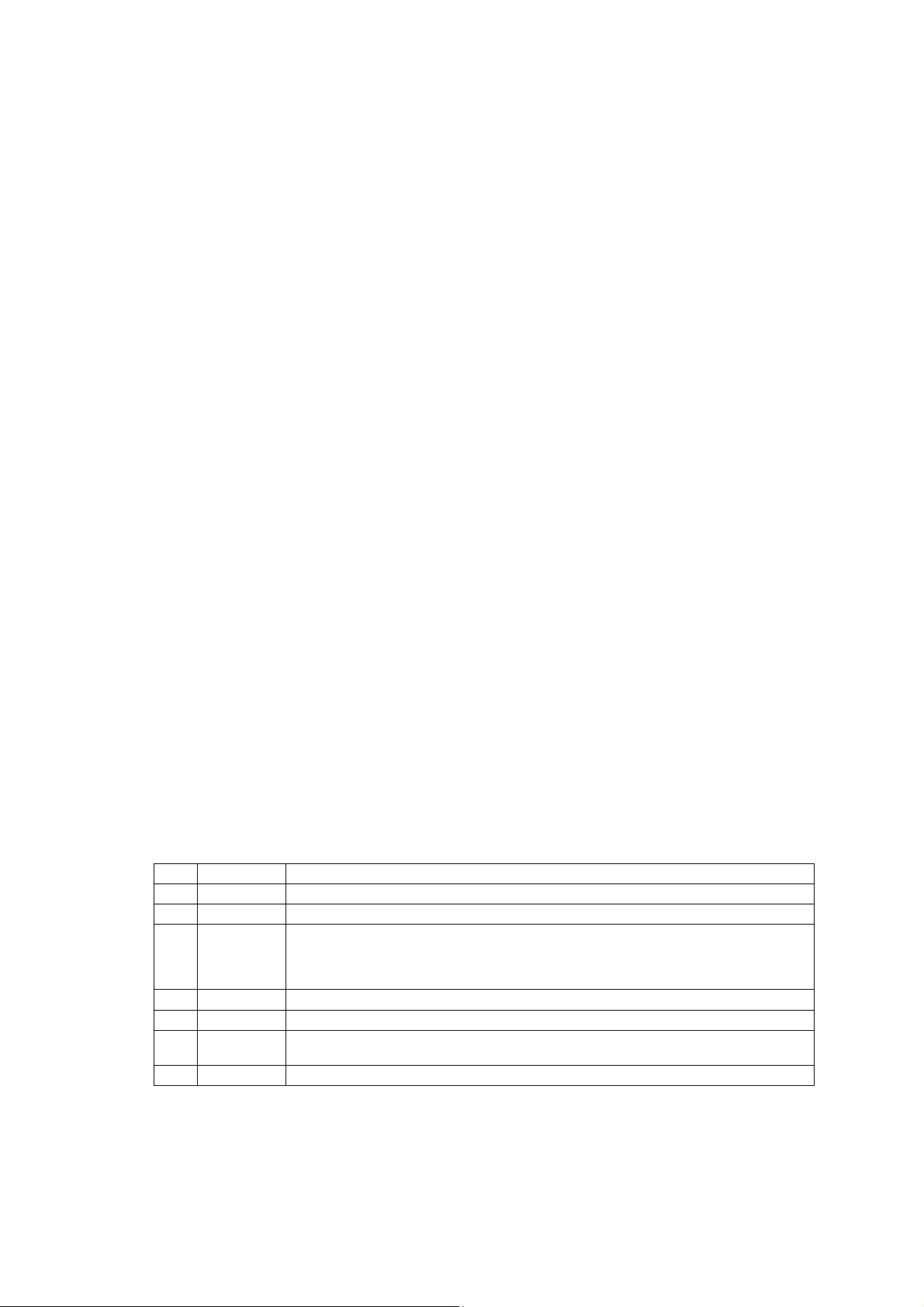
Table 2-1 Modbus Function Codes
. The following paragraphs outline some
Code (decimal) Meaning in Modbus Action
03 Read holding registers Read multiple registers
04 Read input registers Read multiple registers
06 Preset single register Write single register
16 Preset multiple registers Write multiple registers
081 Loop-back test Communications test
1
The EM720 supports only diagnostic code 0 - return query data.
2.4 Exception Responses
The instrument sends an exception response when an error is detected in the received
message. To indicate that the response is notification of an error, the high order bit of
the function code is set to 1.
Implemented exception response codes:
01 - Illegal function
02 - Illegal data address
03 - Illegal data value
04 - Device failure
When the character framing, parity, or redundancy check detects a communication
error, processing of the master's request stops. The instrument will not act on or
respond to the message.
2.5 Modbus Register Addresses
The EM720 Modbus registers are numbered in the range of 0 to 65535. From the
Modbus applications, the EM720 Modbus registers can be accessed by simulating
holding registers of the Modicon 584, 884 or 984 P rogrammable Controller, using a 5digit “4XXXX” or 6-digit “4XXXXX” addressing scheme.
10

To map the EM720 register address to the range of the Modbus holdi ng registers, add
a value of 40001 to the EM720 register address. When a register address exceeds
9999, use a 6-digit addressing scheme by adding 400001 to the EM720 register
address.
2.6 Data Formats
The EM720 uses three data formats to pass data between a master application and the
instrument: 16-bit short integer, 32-bit long integer and 32-bit modulo-10000 formats.
Binary values and counters are always transmitted in 32-bit registers, while analog
values can be read both in 32-bit and in 16-bit scaled registers.
Analog registers 256 through 308 and 6656 through 10935 contain scaled 16-bit
values.
2.6.1 16-bit Scaled Integer Format
16-bit scaled analog data is transmitted in a singl e 16-bit Mo dbus regi ster bei ng scale d
to the range of 0 to 9999. To get a true reading, a reverse conversi on should be done
using the following formula:
)LOHI(X
Y +
=
−×
9999
where:
Y - True reading in engineering units
X - Raw input data in the range of 0 to 9999
LO and HI - Data low and high scales in engineering units
LO
Refer to Section 4 “Data Scales and Units” for applicable data scales and measurement
units. The engineering scales are indicated for every scaled 16-bit register.
The default voltage scale in the device is 144V (120V+20%). It can be changed
through register 242 (see Section 3.1, Device Data Scales), or via the supplemental
PAS software. The recommended voltage scale is 120V+20% = 144V for using with
external PT’s, and 480V+25% = 600V for a direct connection to power line.
CONVERSION EXAMPLES
1. Voltage readings
a) Assume device settings (direct wiring): PT ratio = 1; Voltage scale = 600V (480V + 25%).
Voltage engineering scales (see Section 4) :
HI_ENG = Vmax = 600.0 × PT ratio = 600.0 × 1 = 600.0V
LO_ENG = 0V
If the raw data reading is 2000 then the voltage reading in engineering units will be as follows:
Volts reading = 2000 × (600.0 - 0)/(9999 - 0) + 0 = 120.0V
b) Assume device settings (wiring via PT): PT ratio = 14,400V : 120V = 120; Voltage scale =
144V.
Voltage engineering scales (see Section 4) :
HI_ENG = Vmax = 144.0 × PT ratio = 144 × 120 = 17,280V
LO_ENG = 0V
If the raw data reading is 8314 then the voltage reading in engineering units will be as follows:
Volts reading = 8314 × (17,280 - 0)/9999 + 0 = 14,368V
2. Current readings
Assume device settings: CT primary current = 200A.
11

Current engineering scales (see Section 4) :
HI_ENG = Imax = CT primary current × 2 = 200.00 × 2 = 400.00A
LO_ENG = 0A
If the raw data reading is 250 then the current reading in engineering units will be as follows:
Amps reading = 250 × (400.00 - 0)/(9999 - 0) + 0 = 10.00A
3. Power readings
a) Assume device settings (direct wiring): Wiring 4LL3; PT = 1; CT primary current = 200A;
Voltage scale = 600V.
Active power engineering scales (rounded to whole kW, see Section 4):
HI_ENG = Pmax = Vmax × Imax × 2 = (600.0 × 1) × (200.00 × 2) × 2 = 480,000 W = 480 kW
LO_ENG = -Pmax = -480 kW
If the raw data reading is 5500 then the power reading in engineering units will be as follows:
Watts reading = 5500 × (480 - (-480))/(9999 - 0) + (-480) = 48.1 kW
If the raw data reading is 500 then the power reading in engineering units will be as follows:
Watts reading = 500 × (480 - (-480))/(9999 - 0) + (-480) = -432.0 kW
b) Assume device settings (wiring via PT): Wiring 4LN3; PT = 120; CT primary current = 200A.
Active power engineering scales (rounded to whole kW, see Section 4):
HI_ENG = Pmax = Vmax × Imax × 3 = (600 × 120) × (200.00 × 2) × 3/1000 = 86,400 kW
LO_ENG = -Pmax = -86,400 kW
If the raw data reading is 5500 then the power reading in engineering units will be as follows:
Watts reading = 5500 × (86,400 - (-86,400))/(9999 - 0) + (-86,400) = 8,650 kW
If the raw data reading is 500 then the power reading in engineering units will be as follows:
Watts reading = 500 × (86,400 - (-86,400))/(9999 - 0) + (-86,400) = -77,759 kW
4. Power Factor readings
Power factor engineering scales (see Section 3 .3 ):
HI_ENG = 1.000.
LO_ENG = -1.000.
If the raw data reading is 8900 then the power factor in engineering units will be as follows:
Power factor reading = 8900 × (1.000 - (-1.000))/(9999 - 0) + (-1.000) = 0.78
2.6.2 32-bit Long Integer Format
32-bit long integer data is transmitted in two adjacent 16-bit Modbus registers as
unsigned (UINT32) or signed (INT32) whole numbers. The first register contains the
low-order word (lower 16 bits) and the second register contains the high or der word
(higher 16 bits). The low-order word always starts at an even Modbus address.
The value range for unsigned data is 0 to 4,294,967,295; for signed data the range is 2,147,483,648 to 2,147,483,647.
If your Modbus driver does not support a 32-bit long integer format, you can read the
two 16-bit registers separately, and then convert them into a 32-bi t value as follows
(using C notation):
32-bit value = (signed short) high_order_register × 65536L + (unsigned short) low_order_register
12
EXAMPLES
1. Unsigned 32-bit Values
If you read unsigned Voltage V1 of 69,000V from registers 13952-13953, then the register
readings will be as follows:

(13952) = 3464
(13953) = 1
The 32-bit value is (1 x 65536 + 3464) = 69000V.
2. Signed 32-bit Values
If you read signed kW of -789kW from registers 14336-14337, then the register readings will be:
(14336) = 64747 (unsigned)
(14337) = 65535 (unsigned) or -1(signed value).
To take the high order register as a signed value, compare it with 32767. If the value is less or
equal to 32767, use it as is. If it is greater than 32767, then this is a negative number in a two's
complement code (like in our example) - just subtract it from 65536 to get the original negative
value.
The 32-bit reading is (-1 x 65536 + 64747) = -789kW.
Fractional 32-bit data is transmitted using a decimal pre-multiplier to pass fractional
numbers in an integer format. Fractional numbers are pre-multiplied by 10 to the
power N, where N is the number of digits in the fractional part. For example, the
frequency reading of 50.01 Hz is transmitted as 5001, having been pre-multiplied by
100.
Whenever a data register contains a fractional number, the register measurement unit
is given with a multiplier ×0.1, ×0.01 or ×0.001, showing the weight of the least
significant decimal digit. To get an actual fractional number with specified precision,
multiply the register value by the given multiplier. To write a fractional number into
the register, divide the number by the given multiplier.
2.6.3 32-bit Modulo-10000 Format
Energy counters 287-294 and 301-302 are read in two contiguous 16-bit registers in a
modulo-10000 format. The first (low order) register contains the value mod 10000,
and the second (high order) register contains the value/10000. To get the tr ue energy
reading, the high order register value should be multiplied by 1 0,000 and add ed to th e
low order register.
2.7 User Assignable Registers
The EM720 has 120 user assignable registers in the address range of 0 to 119, any of
which you can map to any register address accessible in the instrument. Registers that
reside in different locations may be accessed by a single request by re-mapping them
to adjacent addresses in the user assignable registers area.
The actual addresses of the assignable registers, which are accesse d via addresses 0
through 119, are specified in the register map (registers 120 through 239), where
register 120 contains the actual address of the register accessed via register 0,
register 121 contains the actual address of the register accessed vi a register 1, and so
on. The assignable registers and the map registers themselves may not be re-mapped.
To build your own register map, write to map registers 120 to 239 the actual
addresses you want to read from or write to via the assignable area (registers 0 to
119). 32-bit long registers should always be ali gned at ev en ad dresses. For example, if
you want to read registers 7136 (1-second V1 voltage, scaled short integer) and
14720-14721 (kWh Import, long integer) via registers 0-2, do the following:
- write 14720 to register 120
- write 14721 to register 121
- write 7136 to register 122
Reading from registers 0-2 will return the kWh reading in regi sters 0 (low 16 bits) and
1 (high 16 bits), and the voltage reading in register 2.
13

2.8 Password Protection
The EM720 has a password protection for setups, cumulative registers and log files
from being changed or cleared via communications. Refer to the EM720 Operation
Manual for details.
A user password must be written into the 32-bit de vice authorization register (44378-
44379) before another write request is issued. If the correct password is not supplied,
the meter will respond to all write requests directed to the meter setup and reset
registers with the exception code 01 (illegal operation). It is recommended to clear the
authorization register after you have completed your changes in order to activate
password protection.
2.9 Data Recording and File Transfers
2.9.1 Log File Organization
Historical files are stored to the non-volatile flash memory. Memory is allocated for
each file statically when you set up your files and will not change unless you reorganize the files. The EM720 automatically performs de-fragmentation of the memory
each time you re-organize your files. This prevents possible leakage of memory caused
by fragmentation.
Data records in a file are arranged in the order of their recording. Each record has a
unique 16-bit sequence number that is incremented modulo 65536 with each new
record. The sequence number can be used to point to a particular record in the file, or
to check the sequence of records when uploading files from the device.
Each file has a write position pointer that indicates the place where the next record will
be recorded, and a read position pointer that indicates the place from where the
current record will be read. Both pointers show sequence numbers of the records they
point to rather than record offsets in the file.
After acknowledging a record you have read, the read pointer automatically advances
to the next record in the file. When the read pointer gets to the record to which the fi le
write pointer points, the end-of-file (EOF) flag is set. It is automatically cleared when a
new record is added to the file, or when you explicitly move the read pointer to any
record within a file.
If a file has a wrap-around attribute (circular file), the most recent records can
overwrite the oldest records. When this happens at the current read position, the read
pointer automatically advances forward in order to point to the oldest record in the file.
The EM720 keeps a separate read pointer for each communication port so that acces s
to the same file through a different port will not affect current active sessions for other
ports.
Multi-section Files
Log files can have one or more (up to 20) sections for multi-channel recording. An
ordinal file consists of a single section. Some files, such as daily profile log files and
waveform log files, are arranged as multi-section files.
A multi-section file is subdivided into multiple sections of the same structure, one
section per recording channel. The number of sections in each file is defined at the
time you set up your files and may not change unless you re-organize the file. Each
section within a multi-section file can be addressed by a section number, or by a
section channel ID.
A multi-section file has a single write position pointer for all sections and stores data in
all sections simultaneously. This means that records with the same sequence number
in all sections are associated with the same event. A multi-section file has also a single
read position pointer for all sections.
Data Log Files
Conventional data log files can store up to 16 measured parameters per a record. Any
data measured by the device can be stored in the log file. The number of parameters
14

that each record will hold and the list of parameters you want to be recorded in the file
can be selected through the Data log setup registers for a particular file.
Recording data to data log files can be triggered through the setpoints, either on a
time basis, or upon any event detected by the setpoints.
Billing/TOU Profile Data Log Files
Data log files #15 and #16 are factory configured for monthly and daily profile logs of
the energy usage and maximum demand registers. A profile log fil e is organized as a
multi-section file that has a separate section for each energy and maximum demand
register. See Sections 3.15-3.16 for more information on the file record s tructure. A
file record stores the summary data (total of all tariffs) and all tariff data for each
configured Billing/TOU register.
The number of sections is taken automatically from your Billing/TOU Registers setup.
Since each Billing/TOU energy register has a shadow maximum demand regi ster, the
number of sections in the file can be twice the number of the allocated Billing/TOU
registers.
Power Quality Statistics Log Files
Data log files #9 and #10 are configured to store the power quality statistics data on a
daily or weekly basis. They are organized as multi-section files. See Sections 3.11-3.14
for more information on the file record structure. You can review the list of parameters
recorded to the files through the file info request/response blocks using info requests
with variation 2 (see Section 3.10).
Waveform Log Files
Waveform log files are organized as multi-section files that store data for each
recording channel in a separate section. A waveform log file can record up to si x AC
channels simultaneously: three voltage and three current waveforms. The number of
sections in a file, or channels that a file can store, is defined when you set up the file.
The channels that a file will record are selected in the waveform log setup. All selected
channels are recorded in successive file sections.
A waveform file has a single read pointer for all sections, so that data from all channels
of a single record can be read together without repositioning the file pointer. When you
point to a particular file record, data from all sections related to the same event are all
available for a read. Moreover, the EM720 takes all channel data for the currently
accessed record to a separate buffer, so that even when the record is overwri tten at
the time of reading, you are still prevented from receiving partially updated data.
A single waveform record for a channel can contain up to 512 points of the sampled
input signal. Refer to the line frequency field in the channel header record to correctly
set up the time scale for the waveforms.
If a waveform log is configured to record more samples per event than a single record
can hold, the waveform recorder will store as many records per event as required to
record the entire event. All waveform records related to the event are merged in a
series and have the same series number, so that they can be plotted together. Each
record within a series has a unique serial number that allows tracking the sequence of
records in a series. A single waveform series can hold up to 81,920 points (2,560
cycles at a rate of 32 samples per cycle) of a sampled AC signal.
2.9.2 File Transfers
File transfer protocol provides both data transfer and information services. File transfer
is performed through two blocks of registers: a 32-word master request bl ock and a
288-word read-only file response block. After a master application has written the
request into the file request block, the requested data is available for a read through
the file response block registers. File transfer functions allow changing the file or
section position in order to point to the desired record.
The information services use separate 8-word file info request and 200-word file info
response blocks. The extended file information is available including current file
pointers’ positions, file contents, the number of records in the file, allocated file size,
time of the last file update, and more.
15

Common File Transfer
Log files can be read either in a sequence record-by-record, or in a random order. Each
Read-File request fills the file response block with the data of the record pointed to by
the file (or section) read pointer. If you want to begin reading a file from a particular
record, which sequence number is known, you can change the pointer position by
issuing the Set-File-Position request with the desired sequence number. If you want to
read a file from the beginning, send the Reset-File-Position request that moves the
pointer to the oldest file record. If you do not change the file position, then you will
continue reading the file from the record following the one you have read the last time
you accessed the file.
You need not explicitly move the file position to the following record if you want to
continue reading a file in sequence after you have uploaded the current record.
Instead, issue an acknowledgment request that automatically advances the file pointer
to the next record, and then read the record data through the file response block.
The file response block can contain more than one record. The number of records
available in the block and the file record size in words are always reported in the block
heading. There are no special rules on how to read records from the file transfer block.
You can read a single record or all records together, or begin reading from the last
record and end with the first record. However, you should remember: 1) after an
acknowledgment, the file position moves to the record following the last one you have
accessed in the file transfer block; and 2) data in the file transfer block does not
change until you either issue an acknowledgment, or explicitly change the file position
by the Set-File-Position or Reset-File-Position requests.
The file transfer is completed after you have read the last record of the file. Before
storing a file record to your database, always check bit 9 in the record status word,
which contains the end-of-file (EOF) flag. This bit set to 1 indicates that the fi le read
pointer does not point to any record within the file, and you should not store any
record that has this bit set. The EOF flag is set only after you have acknowledged the
last record of the file, so that testing for end-of-file requires one extra read. If you
wish to stop the transfer just after storing the last file record, acknowledge the record
and check bit 0 in the record status word. Bit 0 is set to 1 only once when you read the
last record of the file.
The following gives a summary of steps you should do to read an ordinal log file:
1. If you want to begin reading a file from a particular record or from the first record,
use either the Set-File-Position request with the desired record sequence number,
or the Reset-File-Position request. Preset a section number and channel ID to zero.
2. Write the Read-File request wi th a section number and channel ID set to zero.
3. Read the record data from the file response block.
4. Write an acknowledgment for the file. You need not fill all the request fields: onl y
the file function is required. The file pointer will be moved to the next file record.
5. Repeat steps 3-4 until all the file records are read.
Reading Multi-section Data Log Files
In a multi-section data log file, all user requests including an acknowledgment, the
Read-File, Set-File-Position and Reset-File-Position requests, relate to a particular file
section rather than to the file itself. The only request that affects the entire file is the
Erase-File that clears all the file sections together.
A file section can be requested either by a section number, or by a section channel ID.
If you use a channel ID, preset the section number field to 0xFFFF. If a section number
is specified, the channel ID field will not be checked. The device returns bot h fields in
the response block heading, so you can always identify what channel data is being
read from the present file section. If you want to know which channels are recorded to
the file sections, check the file channel mask in the file info block. This is a bitmap that
contains one in a bit position if a channel with an ID equal to the bit number is
recorded to the file, and contains zero if it is not.
The following gives a summary of steps for reading a multi-section data log file:
16

1. If you wish to begin reading a file section from a particular record or from the first
record, use either the Set-File-Position request with the desired record sequence
number, or the Reset-File-Position request. Specify either a section number, or the
channel ID for the section from where you want to read data. If you use a channel
ID, preset the section number field to 0xFFFF.
2. Write the Read-File request with the section number and channel ID as shown in
the previous step.
3. Read the record data from the file response block.
4. Write an acknowledgment for the file. The file section pointer will be moved to the
next record.
5. Repeat steps 3-4 until all the section records are read.
Reading Multi-section Waveform Files
Waveform files can be read as conventional multi-section files in the order described
above. Another way is to take advantage of the fact that waveform files have a single
read pointer for all file sections, so you can read records of all the channels related to
the same event at once without repositioning the file pointer. The following gives a
summary of steps for reading waveform files:
1. If you want to begin reading a file from a particular record or from the first record,
use either the Set-File-Position request with the desired record sequence number,
or the Reset-File-Position request. Preset the section field to zero.
2. Write the Read-File request. Address you request to the first file section (its
number is always zero), or to the first file channel (if you know channel’s ID). If
you use a channel ID, preset the section number field to 0xFFFF.
3. Read the channel’s data from the file response block. Store the recei ved record’s
sequence number.
4. Write the Read-File request for the next file section or channel using the stored
record sequence number. The file response block will be refilled wi th the data for
the requested channel that is related to the record with the same sequence
number.
5. Repeat st eps 3, 4 until all the channel records with the current sequence number
are read.
6. Write an acknowledgment. The file pointer will be moved to the next record.
Repeat steps 2-6 until all the file records are read.
Reading Real-time Waveforms
Real-time waveforms are accessed through the same transfer blocks just like the
waveform log files by addressing file 128. Writing the Read-File request for file 128
provides a simultaneous capture of 6 real-time waveform records – three voltage and
three current waveforms – into a communication buffer that can be read through the
common file response block. The following gives a summary of steps for reading realtime waveforms:
1. Write the Read-File request for file 128. Address you request to the first file section
(its number is always zero), or to the first file channel (if you know channel’s ID).
If you use a channel ID, preset the section number field to 0xFFFF.
2. Read the channel’s data from the file response block.
3. Write the Read-File request for the next file section or channel. The file response
block will be refilled with the data for the requested channel.
4. Repeat steps 3, 4 until all the channel records are read.
5. Write an acknowledgment to rel ease the buffer.
17

2.10 TCP Notification Client
The TCP notification client can establish connections with a remote Modbus/TCP server
and send notification messages either on events, or periodically on a time basis.
Notification messages are sent via a block of 24 Modbus registers using write function
16. The following table shows the message exchange structure.
Modbus
Register Offset
+0-1 Device serial number UINT32
+2-4 Device MAC address CHAR6
+5 Device address UINT16 1 for Ethernet,
+6-7 Device IP address UINT32 Network byte order
+8 Event type UINT16 See F22 in Section 5
+9 Event sequence number UINT16
+10-11 Start event timestamp, seconds UINT32 Local time since Jan 1, 1970
+12-13 Start event timestamp, seconds fraction, in
microseconds
+14-15 End event timestamp, seconds UINT32 Local time since Jan 1, 1970
+16-17 End event timestamp, seconds fraction, in
microseconds
+18 Not used UINT16 Written as 0
+19 Critical trigger ID UINT16 See Table below
+20-21 Critical trigger value UINT32 See Table below
+22-23 Reserved UINT32 Written as 0
Description Type Comment
COM2 port address for GPRS
UINT32
UINT32
The reported trigger type and value depend on the event source and are described in
the following table.
Event Source Trigger Type Trigger Value
Setpoint events Critical setpoint trigger caused setpoint
operation or release (see F12 in Section 5)
PQ events PQ event trigger. For polyphase events, the
worst phase is reported (see Generic Data in
Section 3.4)
Fault events Current phase with highest recorded fault
current (see Generic Data in Section 3.4)
Trigger entering or return value
Maximum fault magnitude on the
reported phase
Maximum fault current magnitude on the
reported phase
18
After receiving a write acknowledgement from a server, a TCP connection is still open
for 10 seconds (20 seconds via GPRS) to give the server an opportunity to access
meter registers through an open socket. It may help you access the meter from
outside your local network when the server is located on another network, or when
using wireless GPRS communications. The notification client will respond to all server
requests as if it were a regular incoming connection.
In case a client connection is not used for following data transfers, it is recommended
for the server to close the connection immediately after sending a write
acknowledgement; otherwise there will be a 10-second delay before the
next notification may be sent.
If there is no activity on the connection socket, it will be closed in 10 seconds. In the
event a connection attempt was unsuccessful, the notification client retries two more
times before announcing a connection failure.
The server’s IP address, port number and starting Modbus register address are
programmable in the meter. To configure and enable the notification client in your
meter via PAS, select Communication Setup in the Meter Setup menu, and click on the
TCP Notification Client Setup tab. See “Setting-up TCP Notification Client” in the meter
manual for more information on the client setup.

Client connections are triggered via programmable setpoints. To send event
notifications to a server, configure a setpoint to respond to desired triggers or to
periodic time events and add the "Send notification" action to the end of the set point
actions list.
Setpoint operation events triggered by regular analog and digital triggers are
reported twice - when the event starts and when it ends, except of the pulsed events
and time triggers that will be reported once. In the start notification message, the
event end timestamp is zeroed, and the critical trigger value indicates its entering
value, while the second notification message gives both the event start and end time
and shows the trigger return value.
In case of triggering notifications with events generated by the PQ and Fault recorders,
like the PQ EVENT, FAULT EVENT, EXTERNAL TRIGGER or FAULT DETECTED tri ggers,
the recorded power quality or/and corresponding fault events are reported instead of
setpoint-triggered notifications. Notification messages contain the fault event start and
end time, a critical phase and the maximum fault magnitude on the reported phase. If
regular triggers are added to the setpoint triggers list, then the setpoint operation
events will also be reported.
19

3 Modbus Register Map
3.1 Modbus Setup Registers
Address Point ID Description Options/Range Units Type R/W Notes
Modbus Assignable Registers
0-119
+0 Register 0 contents 0-65535 UINT16 R/W
+1 Register 1 contents 0-65535 UINT16 R/W
...
+119 Register 119 contents 0-65535 UINT16 R/W
Assignable Registers Map
120-239
+0 Mapped register 0 address 0-65535 UINT16 R/W
+1 Mapped register 1 address 0-65535 UINT16 R/W
+119 Mapped register 119 address 0-65535 UINT16 R/W
Modbus Conversion Scales
240 Low raw scale 0 UINT16 R
241 High raw scale 9999 UINT16 R
Device Data Scales
242 Voltage scale, in secondary volts 60-600 (default 144V) 1V UINT16 R/W
243 Current scale, in secondary amps 10-500 (default is CT secondary
current × Current Overload)
×0.1A
UINT16 R/W
20

3.2 16-bit Scaled Analog Registers and Energy Counters - Basic Register Set
Address Point ID Description
Low and High Scales
256-308
+0 0x1100 V1/V12 Voltage 0-Vmax U1 UINT16 R 1
+1 0x1101 V2/V23 Voltage 0-Vmax U1 UINT16 R 1
+2 0x1102 V3/V31 Voltage 0-Vmax U1 UINT16 R 1
+3 0x1103 I1 Current 0-Imax U2 UINT16 R
+4 0x1104 I2 Current 0-Imax U2 UINT16 R
+5 0x1105 I3 Current 0-Imax U2 UINT16 R
+6 0x1106 kW L1 -Pmax-Pmax U3 INT16 R
+7 0x1107 kW L2 -Pmax-Pmax U3 INT16 R
+8 0x1108 kW L3 -Pmax-Pmax U3 INT16 R
+9 0x1109 kvar L1 -Pmax-Pmax U3 INT16 R
+10 0x110A kvar L2 -Pmax-Pmax U3 INT16 R
+11 0x110B kvar L3 -Pmax-Pmax U3 INT16 R
+12 0x110C kVA L1 -Pmax-Pmax U3 UINT16 R
+13 0x110D kVA L2 -Pmax-Pmax U3 UINT16 R
+14 0x110E kVA L3 -Pmax-Pmax U3 UINT16 R
+15 0x110F Power factor L1 -1.000-1.000 0.001 INT16 R
+16 0x1110 Power factor L2 -1.000-1.000 0.001 INT16 R
+17 0x1111 Power factor L3 -1.000-1.000 0.001 INT16 R
+18 0x1403 Total PF -1.000-1.000 0.001 INT16 R
+19 0x1400 Total kW -Pmax-Pmax U3 INT16 R
+20 0x1401 Total kvar -Pmax-Pmax U3 INT16 R
+21 0x1402 Total kVA -Pmax-Pmax U3 UINT16 R
+22 0x1501 In (neutral) Current 0-Imax U4 UINT16 R
+23 0x1502 Frequency 45.00-65.00 0.01 Hz UINT16 R
+24 0x3709 Maximum kW import sliding window demand -Pmax-Pmax U3 UINT16 R
+25 0x160F kW import accumulated demand -Pmax-Pmax U3 UINT16 R
+26 0x370B Maximum kVA sliding window demand -Pmax-Pmax U3 UINT16 R
+27 0x1611 kVA accumulated demand -Pmax-Pmax U3 UINT16 R
+28 0x3703 I1 Maximum ampere demand 0-Imax U2 UINT16 R
+29 0x3704 I2 Maximum ampere demand 0-Imax U2 UINT16 R
+30 0x3705 I3 Maximum ampere demand 0-Imax U2 UINT16 R
+31 kWh import (low) 0-9999
+32 kWh import (high) 0-9999
+33 kWh export (low) 0-9999
+34 kWh export (high) 0-9999
+35 +kvarh net (low) 0-9999
+36 +kvarh net (high) 0-9999
+37 -kvarh net (low) 0-9999
2
Units2
×0.1 kWh
×1 MWh
×0.1 kWh
×1 MWh
×0.1 kvarh
×1 Mvarh
×0.1 kvarh
UINT16 R 6
UINT16 R 6
UINT16 R 6
UINT16 R 6
UINT16 R
UINT16 R
UINT16 R
Type R/W Notes
4, 6
4, 6
5, 6
21

Address Point ID Description
+38 -kvarh net (high) 0-9999
Low and High Scales
2
Units2
×1 Mvarh
Type R/W Notes
UINT16 R
5, 6
+39 0x1112 V1/V12 Voltage THD 0-999.9 0.1% UINT16 R 3
+40 0x1113 V2/V23 Voltage THD 0-999.9 0.1% UINT16 R 3
+41 0x1114 V3/V31 Voltage THD 0-999.9 0.1% UINT16 R 3
+42 0x1115 I1 Current THD 0-999.9 0.1% UINT16 R
+43 0x1116 I2 Current THD 0-999.9 0.1% UINT16 R
+44 0x1117 I3 Current THD 0-999.9 0.1% UINT16 R
+45 kVAh (low) 0-9999
+46 kVAh (high) 0-9999
×0.1 kVAh
×1 MVAh
UINT16 R 6
UINT16 R 6
3
3
3
+47 0x1609 Present kW import sliding window demand -Pmax-Pmax U3 UINT16 R
+48 0x160B Present kVA sliding window demand -Pmax-Pmax U3 UINT16 R
+49 0x1615 PF (import) at Max. kVA sliding window demand 0-1.000 0.001 UINT16 R
+50 0x111B I1 Current TDD 0-100.0 0.1% UINT16 R
+51 0x111C I2 Current TDD 0-100.0 0.1% UINT16 R
+52 0x111D I3 Current TDD 0-100.0 0.1% UINT16 R
3
3
3
NOTES:
1
When the 4LN3 or 3LN3 wiring mode is selected, the voltages will be line-to-neutral; for any other wiring mode, they will be line-to-line voltages.
2
All analog registers except of harmonics are 1- second average values. For volts, amps and power scales and units, refer to Section 4 ”Data Scales and Units”. For analog data scaling
formulas and examples, see Section 2.6.1, “16-bit Scaled Integer Format”.
3
On a 3-s interval.
4
Positive readings of kvarh net.
5
Negative readings of kvarh net.
6
If you use these energy registers instead of 32-bit registers, limit the energy roll value to 8 digits (see Device Options Setup) to avoid early overflow.
22
3.3 16-bit Scaled Analog Registers, Binary Registers and Counters
Address Point ID Description
3584 0x0000 None 0 UINT16 R 3616 0x0080 Setpoint Status 0x0000-0xFFFF UINT16 R Bitmap: 0=released, 1=operated
3648-3649 Special Inputs
+0 0x0100 Not used 0 UINT16 R
+1 0x0101 Phase rotation order 0=error, 1=positive (ABC),
3776 0x0300 Event Flags 0x0000-0x00FF UINT16 R Bitmap: 0=OFF, 1=ON 3968 0x0600 Digital Inputs 0x0000-0x00FF UINT16 R Bitmap: 0=open, 1=closed 4096 0x0800 Relay Outputs 0x0000-0x000F UINT16 R Bitmap: 0=open, 1=closed
4224-4239 Counters
+0,1 0x0A00 Counter #1 0-999,999,999 UINT32 R/W
+2,3 0x0A01 Counter #2 0-999,999,999 UINT32 R/W
+4,5 0x0A02 Counter #3 0-999,999,999 UINT32 R/W
+6,7 0x0A03 Counter #4 0-999,999,999 UINT32 R/W
+8,9 0x0A04 Counter #5 0-999,999,999 UINT32 R/W
+10,11 0x0A05 Counter #6 0-999,999,999 UINT32 R/W
+12,13 0x0A06 Counter #7 0-999,999,999 UINT32 R/W
+14,15 0x0A07 Counter #8 0-999,999,999 UINT32 R/W
4320-4344 1/2-Cycle Values
+0 0x0B80 V1 Voltage 0-Vmax U1 UINT16 R 1
+1 0x0B81 V2 Voltage 0-Vmax U1 UINT16 R 1
+2 0x0B82 V3 Voltage 0-Vmax U1 UINT16 R 1
+3 0x0B83 Not used 0 U1 UINT16 R
+4 0x0B84 V12 Voltage 0-Vmax U1 UINT16 R
+5 0x0B85 V23 Voltage 0-Vmax U1 UINT16 R
+5 0x0B86 V31 Voltage 0-Vmax U1 UINT16 R
+7 0x0B87 I1 Current 0-Imax U4 UINT16 R
+8 0x0B88 I2 Current 0-Imax U4 UINT16 R
+9 0x0B89 I3 Current 0-Imax U4 UINT16 R
+10 0x0B8A I4 Current 0-I4max U4 UINT16 R
+11 0x0B8B In Current 0-Imax U4 UINT16 R
+12 0x0B8C Not used 0 UINT16 R
+13 0x0B8D Not used 0 UINT16 R
+14 0x0B8E Not used 0 UINT16 R
+15 0x0B8F Not used 0 UINT16 R
+16 0x0B90 Not used 0 UINT16 R
+17 0x0B91 Zero-sequence voltage 0-Vmax U1 UINT16 R
+18 0x0B92 Zero-sequence current 0-Imax U4 UINT16 R
+19 0x0B93 Not used 0 UINT16 R
+20 0x0B94 Voltage unbalance 0-300.0 0.1% UINT16 R
Low and High Scales
2=negative (CBA)
3
Units3
Type R/W Notes
UINT16 R
23

Address Point ID Description
Low and High Scales
3
Units3
Type R/W Notes
+21 0x0B95 Current unbalance 0-300.0 0.1% UINT16 R
+22 0x0B96 Not used 0 UINT16 R
+23 0x0B97 Not used 0 UINT16 R
+24 0x0B98 Frequency (1-cycle) 0-100.00 0.01Hz UINT16 R
4352-4390 1-Cycle Phase Values
+0 0x0C00 V1/V12 Voltage 0-Vmax U1 UINT16 R 1
+1 0x0C01 V2/V23 Voltage 0-Vmax U1 UINT16 R 1
+2 0x0C02 V3/V31 Voltage 0-Vmax U1 UINT16 R 1
+3 0x0C03 I1 Current 0-Imax U4 UINT16 R
+4 0x0C04 I2 Current 0-Imax U4 UINT16 R
+5 0x0C05 I3 Current 0-Imax U4 UINT16 R
+6 0x0C06 kW L1 -Pmax-Pmax U3 INT16 R
+7 0x0C07 kW L2 -Pmax-Pmax U3 INT16 R
+8 0x0C08 kW L3 -Pmax-Pmax U3 INT16 R
+9 0x0C09 kvar L1 -Pmax-Pmax U3 INT16 R
+10 0x0C0A kvar L2 -Pmax-Pmax U3 INT16 R
+11 0x0C0B kvar L3 -Pmax-Pmax U3 INT16 R
+12 0x0C0C kVA L1 0-Pmax U3 UINT16 R
+13 0x0C0D kVA L2 0-Pmax U3 UINT16 R
+14 0x0C0E kVA L3 0-Pmax U3 UINT16 R
+15 0x0C0F Power factor L1 -1.000-1.000 0.001 INT16 R
+16 0x0C10 Power factor L2 -1.000-1.000 0.001 INT16 R
+17 0x0C11 Power factor L3 -1.000-1.000 0.001 INT16 R
+18 0x0C12 V1/V12 Voltage THD 0-999.9 0.1% UINT16 R
+19 0x0C13 V2/V23 Voltage THD 0-999.9 0.1% UINT16 R
+20 0x0C14 V3/V31 Voltage THD 0-999.9 0.1% UINT16 R
+21 0x0C15 I1 Current THD 0-999.9 0.1% UINT16 R
+22 0x0C16 I2 Current THD 0-999.9 0.1% UINT16 R
+23 0x0C17 I3 Current THD 0-999.9 0.1% UINT16 R
2, 5
2, 5
2, 5
5
5
5
+24 0x0C18 I1 K-Factor 1.0-999.9 0.1 UINT16 R 5
+25 0x0C19 I2 K-Factor 1.0-999.9 0.1 UINT16 R 5
+26 0x0C1A I3 K-Factor 1.0-999.9 0.1 UINT16 R 5
+27 0x0C1B I1 Current TDD 0-100.0 0.1% UINT16 R
+28 0x0C1C I2 Current TDD 0-100.0 0.1% UINT16 R
+29 0x0C1D I3 Current TDD 0-100.0 0.1% UINT16 R
5
5
5
+30 0x0C1E V12 Voltage 0-Vmax U1 UINT16 R
+31 0x0C1F V23 Voltage 0-Vmax U1 UINT16 R
+32 0x0C20 V31 Voltage 0-Vmax U1 UINT16 R
4416-4427 1-Cycle Low Phase Values
+0 0x0D00 Low voltage 0-Vmax U1 UINT16 R 1
+1 0x0D01 Low current 0-Imax U4 UINT16 R
+2 0x0D02 Low kW -Pmax-Pmax U3 INT16 R
+3 0x0D03 Low kvar -Pmax-Pmax U3 INT16 R
24

Address Point ID Description
Low and High Scales
3
Units3
Type R/W Notes
+4 0x0D04 Low kVA 0-Pmax U3 UINT16 R
+5 0x0D05 Low PF Lag 0-1.000 0.001 UINT16 R
+5 0x0D06 Low PF Lead 0-1.000 0.001 UINT16 R
+7 0x0D07 Low voltage THD 0-999.9 0.1% UINT16 R
+8 0x0D08 Low current THD 0-999.9 0.1% UINT16 R
+9 0x0D09 Low K-Factor 1.0-999.9 0.1 UINT16 R
+10 0x0D0A Low current TDD 0-100.0 0.1% UINT16 R
2, 5
5
5
5
+11 0x0D0B Low L-L voltage 0-Vmax U1 UINT16 R 5
4480-4491 1-Cycle High Phase Values
+0 0x0E00 High voltage 0-Vmax U1 UINT16 R 1
+1 0x0E01 High current 0-Imax U4 UINT16 R
+2 0x0E02 High kW -Pmax-Pmax U3 INT16 R
+3 0x0E03 High kvar -Pmax-Pmax U3 INT16 R
+4 0x0E04 High kVA 0-Pmax U3 UINT16 R
+5 0x0E05 High PF Lag 0-1.000 0.001 UINT16 R
+5 0x0E06 High PF Lead 0-1.000 0.001 UINT16 R
+7 0x0E07 High voltage THD 0-999.9 0.1% UINT16 R
+8 0x0E08 High current THD 0-999.9 0.1% UINT16 R
2, 5
5
+9 0x0E09 High K-Factor 1.0-999.9 0.1 UINT16 R 5
+10 0x0E0A High current TDD 0-100.0 0.1% UINT16 R
+11 0x0E0B High L-L voltage 0-Vmax U1 UINT16 R
5
5
4544-4556 1-Cycle Total Values
+0 0x0F00 Total kW -Pmax-Pmax U3 INT16 R
+1 0x0F01 Total kvar -Pmax-Pmax U3 INT16 R
+2 0x0F02 Total kVA 0-Pmax U3 UINT16 R
+3 0x0F03 Total PF -1.000-1.000 0.001 INT16 R
+4 0x0F04 Total PF lag 0-1.000 0.001 UINT16 R
+5 0x0F05 Total PF lead 0-1.000 0.001 UINT16 R
+5 0x0F06 Total kW import 0-Pmax U3 UINT16 R
+7 0x0F07 Total kW export 0-Pmax U3 UINT16 R
+8 0x0F08 Total kvar import 0-Pmax U3 UINT16 R
+9 0x0F09 Total kvar export 0-Pmax U3 UINT32 R
+10 0x0F0A 3-phase average L-N/L-L voltage 0-Vmax U1 UINT16 R
1
+11 0x0F0B 3-phase average L-L voltage 0-Vmax U1 UINT16 R
+12 0x0F0C 3-phase average current 0-Imax U2 UINT16 R
4608-4612 1-Cycle Auxiliary Values
+0 0x1000 I4 Current 0-I4max U4 UINT16 R
+1 0x1001 In (neutral) Current 0-Imax U4 UINT16 R
+2 0x1002 Frequency 0-Fmax 0.01Hz UINT16 R
+3 0x1003 Voltage unbalance 0-300.0 0.1% UINT16 R
+4 0x1004 Current unbalance 0-300.0 0.1% UINT16 R
+5 0x1005 Not used 0 UINT16 R
+6 0x1006 Not used 0 UINT16 R
25

Address Point ID Description
Low and High Scales
3
Units3
Type R/W Notes
4640-4655 Phasor
+0 0x1080 V1/V12 Voltage magnitude 0-Vmax U1 UINT16 R
+1 0x1081 V2/V23 Voltage magnitude 0-Vmax U1 UINT16 R
+2 0x1082 V3/V31 Voltage magnitude 0-Vmax U1 UINT16 R
2
2
2
+3 0x1083 Not used UINT16 R
+4 0x1084 I1 Current magnitude 0-Imax U4 UINT16 R
+5 0x1085 I2 Current magnitude 0-Imax U4 UINT16 R
+6 0x1086 I3 Current magnitude 0-Imax U4 UINT16 R
+7 0x1087 I4 Current magnitude 0-I4max U4 UINT16 R
+8 0x1088 V1/V12 Voltage angle -180.0-180.0 0.1º INT16 R
+9 0x1089 V2/V23 Voltage angle -180.0-180.0 0.1º INT16 R
+10 0x108A V3/V31 Voltage angle -180.0-180.0 0.1º INT16 R
2
2
2
+11 0x108B Not used INT16 R
+12 0x108C I1 Current angle -180.0-180.0 0.1º INT16 R
+13 0x108D I2 Current angle -180.0-180.0 0.1º INT16 R
+14 0x108E I3 Current angle -180.0-180.0 0.1º INT16 R
+15 0x108F I4 Current angle -180.0-180.0 0.1º INT16 R
4672-4710 1-Second Phase Values
+0 0x1100 V1/V12 Voltage 0-Vmax U1 UINT16 R 1
+1 0x1101 V2/V23 Voltage 0-Vmax U1 UINT16 R 1
+2 0x1102 V3/V31 Voltage 0-Vmax U1 UINT16 R 1
+3 0x1103 I1 Current 0-Imax U2 UINT16 R
+4 0x1104 I2 Current 0-Imax U2 UINT16 R
+5 0x1105 I3 Current 0-Imax U2 UINT16 R
+6 0x1106 kW L1 -Pmax-Pmax U3 INT16 R
+7 0x1107 kW L2 -Pmax-Pmax U3 INT16 R
+8 0x1108 kW L3 -Pmax-Pmax U3 INT16 R
+9 0x1109 kvar L1 -Pmax-Pmax U3 INT16 R
+10 0x110A kvar L2 -Pmax-Pmax U3 INT16 R
+11 0x110B kvar L3 -Pmax-Pmax U3 INT16 R
+12 0x110C kVA L1 0-Pmax U3 UINT16 R
+13 0x110D kVA L2 0-Pmax U3 UINT16 R
+14 0x110E kVA L3 0-Pmax U3 UINT16 R
+15 0x110F Power factor L1 -1.000-1.000 0.001 INT16 R
+16 0x1110 Power factor L2 -1.000-1.000 0.001 INT16 R
+17 0x1111 Power factor L3 -1.000-1.000 0.001 INT16 R
+18 0x1112 V1/V12 Voltage THD 0-999.9 0.1% UINT16 R
+19 0x1113 V2/V23 Voltage THD 0-999.9 0.1% UINT16 R
+20 0x1114 V3/V31 Voltage THD 0-999.9 0.1% UINT16 R
+21 0x1115 I1 Current THD 0-999.9 0.1% UINT16 R
+22 0x1116 I2 Current THD 0-999.9 0.1% UINT16 R
+23 0x1117 I3 Current THD 0-999.9 0.1% UINT16 R
2, 6
2, 6
2, 6
6
6
6
+24 0x1118 I1 K-Factor 1.0-999.9 0.1 UINT16 R 6
26

Address Point ID Description
Low and High Scales
3
Units3
Type R/W Notes
+25 0x1119 I2 K-Factor 1.0-999.9 0.1 UINT16 R 6
+26 0x111A I3 K-Factor 1.0-999.9 0.1 UINT16 R 6
+27 0x111B I1 Current TDD 0-100.0 0.1% UINT16 R
+28 0x111C I2 Current TDD 0-100.0 0.1% UINT16 R
+29 0x111D I3 Current TDD 0-100.0 0.1% UINT16 R
6
6
6
+30 0x111E V12 Voltage 0-Vmax U1 UINT16 R
+31 0x111F V23 Voltage 0-Vmax U1 UINT16 R
+32 0x1120 V31 Voltage 0-Vmax U1 UINT16 R
+33 0x1121 Not used 0 UINT16 R
+34 0x1122 Not used 0 UINT16 R
+35 0x1123 Not used 0 UINT16 R
+36 0x1124 V1x Voltage 0-Vmax U1 UINT16 R Transient recorder V1 channel
+37 0x1125 V2x Voltage 0-Vmax U1 UINT16 R Transient recorder V2 channel
+38 0x1126 V3x Voltage 0-Vmax U1 UINT16 R Transient recorder V3 channel
4736-4749 1-Second Low Phase Values
+0 0x1200 Low voltage 0-Vmax U1 UINT16 R 1
+1 0x1201 Low current 0-Imax U2 UINT16 R
+2 0x1202 Low kW -Pmax-Pmax U3 INT16 R
+3 0x1203 Low kvar -Pmax-Pmax U3 INT16 R
+4 0x1204 Low kVA 0-Pmax U3 UINT16 R
+5 0x1205 Low PF Lag 0-1.000 0.001 UINT16 R
+5 0x1206 Low PF Lead 0-1.000 0.001 UINT16 R
+7 0x1207 Low voltage THD 0-999.9 0.1% UINT16 R
+8 0x1208 Low current THD 0-999.9 0.1% UINT16 R
2, 6
6
+9 0x1209 Low K-Factor 1.0-999.9 0.1 UINT16 R 6
+10 0x120A Low current TDD 0-100.0 0.1% UINT16 R
6
+11 0x120B Low L-L voltage 0-Vmax U1 UINT16 R
4768-4783 3-Second Powers
+0 0x1280 kW L1 -Pmax-Pmax U3 INT16 R
+1 0x1281 kW L2 -Pmax-Pmax U3 INT16 R
+2 0x1282 kW L3 -Pmax-Pmax U3 INT16 R
+3 0x1283 kvar L1 -Pmax-Pmax U3 INT16 R
+4 0x1284 kvar L2 -Pmax-Pmax U3 INT16 R
+5 0x1285 kvar L3 -Pmax-Pmax U3 INT16 R
+6 0x1286 kVA L1 0-Pmax U3 UINT16 R
+7 0x1287 kVA L2 0-Pmax U3 UINT16 R
+8 0x1288 kVA L3 0-Pmax U3 UINT16 R
+9 0x1289 Power factor L1 -1.000-1.000 0.001 INT16 R
+10 0x128A Power factor L2 -1.000-1.000 0.001 INT16 R
+11 0x128B Power factor L3 -1.000-1.000 0.001 INT16 R
+12 0x128C Total kW -Pmax-Pmax U3 INT16 R
+13 0x128D Total kvar -Pmax-Pmax U3 INT16 R
+14 0x128E Total kVA 0-Pmax U3 UINT16 R
27

Address Point ID Description
Low and High Scales
3
Units3
Type R/W Notes
+15 0x128F Total PF -1.000-1.000 0.001 INT16 R
4800-4813 1-Second High Phase Values
+0 0x1300 High voltage 0-Vmax U1 UINT16 R 1
+1 0x1301 High current 0-Imax U2 UINT16 R
+2 0x1302 High kW -Pmax-Pmax U3 INT16 R
+3 0x1303 High kvar -Pmax-Pmax U3 INT16 R
+4 0x1304 High kVA 0-Pmax U3 UINT16 R
+5 0x1305 High PF Lag 0-1.000 0.001 UINT16 R
+5 0x1306 High PF Lead 0-1.000 0.001 UINT16 R
+7 0x1307 High voltage THD 0-999.9 0.1% UINT16 R
+8 0x1308 High current THD 0-999.9 0.1% UINT16 R
2, 6
6
+9 0x1309 High K-Factor 1.0-999.9 0.1 UINT16 R 6
+10 0x130A High current TDD 0-100.0 0.1% UINT16 R
6
+11 0x130B High L-L voltage 0-Vmax U1 UINT16 R
4864-4885 1-Second Total Values
+0 0x1400 Total kW -Pmax-Pmax U3 INT16 R
+1 0x1401 Total kvar -Pmax-Pmax U3 INT16 R
+2 0x1402 Total kVA 0-Pmax U3 UINT16 R
+3 0x1403 Total PF -1.000-1.000 0.001 INT16 R
+4 0x1404 Total PF lag 0-1.000 0.001 UINT16 R
+5 0x1405 Total PF lead 0-1.000 0.001 UINT16 R
+5 0x1406 Total kW import 0-Pmax U3 UINT16 R
+7 0x1407 Total kW export 0-Pmax U3 UINT16 R
+8 0x1408 Total kvar import 0-Pmax U3 UINT16 R
+9 0x1409 Total kvar export 0-Pmax U3 UINT16 R
+10 0x140A 3-phase average L-N/L-L voltage 0-Vmax U1 UINT16 R
1
+11 0x140B 3-phase average L-L voltage 0-Vmax U1 UINT16 R
+12 0x140C 3-phase average current 0-Imax U2 UINT16 R
+13 0x140D Not used 0 UINT16 R
+14 0x140E Total kW Fe losses -Pmax-Pmax U3 UINT16 R
+15 0x140F Total kW Cu losses -Pmax-Pmax U3 UINT16 R
+16 0x1410 Total kvar Fe losses -Pmax-Pmax U3 UINT16 R
+17 0x1411 Total kvar Cu losses -Pmax-Pmax U3 UINT16 R
+18 0x1412 Total uncompensated kW -Pmax-Pmax U3 INT16 R
+19 0x1413 Total uncompensated kvar -Pmax-Pmax U3 INT16 R
+20 0x1414 Total uncompensated kVA 0-Pmax U3 UINT16 R
+21 0x1415 Total uncompensated PF -1.000-1.000 0.001 INT16 R
4928-4937 1-Second Auxiliary Values
+0 0x1500 I4 Current 0-I4max U4 UINT16 R
+1 0x1501 In (neutral) Current 0-Imax U4 UINT16 R
+2 0x1502 Frequency 0-Fmax 0.01Hz UINT16 R
+3 0x1503 Voltage unbalance 0-300.0 0.1% UINT16 R
+4 0x1504 Current unbalance 0-300.0 0.1% UINT16 R
28

Address Point ID Description
Low and High Scales
3
Units3
Type R/W Notes
+5 0x1505 Battery DC voltage 0-9999.00 0.01V UINT16 R
+6 0x1506 Not used 0 UINT16 R
+7 0x1507 Not used 0 UINT16 R
+8 0x1508 V4x (neutral-ground) voltage 0-Vmax U1 UINT16 R Transient recorder Vn channel
+9 0x1509 Internal temperature -200.0 to 200.0 0.1ºC INT16 R
4960-4971 Present Harmonic Demands
+0 0x1580 V1/V12 THD demand 0-999.9 0.1% UINT16 R
+1 0x1581 V2/V23 THD demand 0-999.9 0.1% UINT16 R
+2 0x1582 V3/V31 THD demand 0-999.9 0.1% UINT16 R
2
2
2
+3 0x1583 Not used UINT16 R
+4 0x1584 I1 THD demand 0-999.9 0.1% UINT16 R
+5 0x1585 I2 THD demand 0-999.9 0.1% UINT16 R
+6 0x1586 I3 THD demand 0-999.9 0.1% UINT16 R
+7 0x1587 I4 THD demand 0-999.9 0.1% UINT16 R
+8 0x1588 I1 TDD demand 0-100.0 0.1% UINT16 R
+9 0x1589 I2 TDD demand 0-100.0 0.1% UINT16 R
+10 0x158A I3 TDD demand 0-100.0 0.1% UINT16 R
+11 0x158B I4 TDD demand 0-100.0 0.1% UINT16 R
4992-5021 Present Demands
+0 0x1600 V1/V12 Volt demand 0-Vmax U1 UINT16 R
+1 0x1601 V2/V23 Volt demand 0-Vmax U1 UINT16 R
+2 0x1602 V3/V31 Volt demand 0-Vmax U1 UINT16 R
2
2
2
+3 0x1603 I1 Ampere demand 0-Imax U2 UINT16 R
+4 0x1604 I2 Ampere demand 0-Imax U2 UINT16 R
+5 0x1605 I3 Ampere demand 0-Imax U2 UINT16 R
+6 0x1606 kW import block demand 0-Pmax U3 UINT16 R
+7 0x1607 kvar import block demand 0-Pmax U3 UINT16 R
+8 0x1608 kVA block demand 0-Pmax U3 UINT16 R
+9 0x1609 kW import sliding window demand 0-Pmax U3 UINT16 R
+10 0x160A kvar import sliding window demand 0-Pmax U3 UINT16 R
+11 0x160B kVA sliding window demand 0-Pmax U3 UINT16 R
+12 0x160C Not used UINT16 R
+13 0x160D Not used UINT16 R
+14 0x160E Not used UINT16 R
+15 0x160F kW import accumulated demand 0-Pmax U3 UINT16 R
+16 0x1610 kvar import accumulated demand 0-Pmax U3 UINT16 R
+17 0x1611 kVA accumulated demand 0-Pmax U3 UINT16 R
+18 0x1612 kW import predicted sliding window demand 0-Pmax U3 UINT16 R
+19 0x1613 kvar import predicted sliding window demand 0-Pmax U3 UINT16 R
+20 0x1614 kVA predicted sliding window demand 0-Pmax U3 UINT16 R
+21 0x1615 PF (import) at Max. kVA sliding window demand 0-1.000 0.001 UINT16 R
+22 0x1616 kW export block demand 0-Pmax U3 UINT16 R
+23 0x1617 kvar export block demand 0-Pmax U3 UINT16 R
29

Address Point ID Description
+24 0x1618 kW export sliding window demand 0-Pmax U3 UINT16 R
+25 0x1619 kvar export sliding window demand 0-Pmax U3 UINT16 R
+26 0x161A kW export accumulated demand 0-Pmax U3 UINT16 R
+27 0x161B kvar export accumulated demand 0-Pmax U3 UINT16 R
+28 0x161C kW export predicted sliding window demand 0-Pmax U3 UINT16 R
+29 0x161D kvar export predicted sliding window demand 0-Pmax U3 UINT16 R
+30 0x161E Not used 0 UINT16 R
+31 0x161F Not used 0 UINT16 R
+32 0x1620 Not used 0 UINT16 R
+33 0x1621 I4 ampere demand 0-Imax U4 UINT16 R
5056-5073 Instrumentation Total Energies
+0,1 0x1700 kWh import 0-999,999,999 0.1 kWh UINT32 R
+2,3 0x1701 kWh export 0-999,999,999 0.1 kWh UINT32 R
+4,5 0x1702 kWh net -999,999,999-999,999,999 0.1 kWh INT32 R
+6,7 0x1703 Not used R
+8,9 0x1704 kvarh import 0-999,999,999 0.1 kvarh UINT32 R
+10,11 0x1705 kvarh export 0-999,999,999 0.1 kvarh UINT32 R
+12,13 0x1706 kvarh net -999,999,999-999,999,999 0.1 kvarh INT32 R
+14,15 0x1707 Not used R
+16,17 0x1708 kVAh total 0-999,999,999 0.1 kVAh UINT32 R
+18,19 0x1709 Not used UINT32 R
+20,21 0x170A Not used UINT32 R
+22,23 0x170B kVAh import 0-999,999,999 0.1 kVAh UINT32 R
+24,25 0x170C kVAh export 0-999,999,999 0.1 kVAh UINT32 R
+26,27 0x170D Not used UINT32 R
+28,29 0x170E Not used UINT32 R
+30,31 0x170F Not used UINT32 R
+32,33 0x1710 Not used UINT32 R
+34,35 0x1711 Not used UINT32 R
+36,37 0x1712 kvarh Q1 0-999,999,999 0.1 kvarh UINT32 R
+38,39 0x1713 kvarh Q2 0-999,999,999 0.1 kvarh UINT32 R
+40,41 0x1714 kvarh Q3 0-999,999,999 0.1 kvarh UINT32 R
+42,43 0x1715 kvarh Q4 0-999,999,999 0.1 kvarh UINT32 R
5152-5161 Symmetrical Components
+0 0x1880 Positive-sequence voltage 0-Vmax U1 UINT16 R
+1 0x1881 Negative-sequence voltage 0-Vmax U1 UINT16 R
+2 0x1882 Zero-sequence voltage 0-Vmax U1 UINT16 R
+3 0x1883 Negative-sequence voltage unbalance 0-300.0 0.1% UINT16 R
+4 0x1884 Zero-sequence voltage unbalance 0-300.0 0.1% UINT16 R
+5 0x1885 Positive-sequence current 0-Imax U4 UINT16 R
+6 0x1886 Negative-sequence current 0-Imax U4 UINT16 R
+7 0x1887 Zero-sequence current 0-Imax U4 UINT16 R
+8 0x1888 Negative-sequence current unbalance 0-300.0 0.1% UINT16 R
Low and High Scales
3
Units3
Type R/W Notes
30

Address Point ID Description
Low and High Scales
3
Units3
Type R/W Notes
+9 0x1889 Zero-sequence current unbalance 0-300.0 0.1% UINT16 R
5184-5233 V1/V12 Harmonic Distortion
2
+0 0x1900 H01 Harmonic distortion 0-100.00 0.01% UINT16 R
+1 0x1901 H02 Harmonic distortion 0-100.00 0.01% UINT16 R
...
+49 0x1931 H50 Harmonic distortion 0-100.00 0.01% UINT16 R
5248-5297 V2/V23 Harmonic Distortion
2
+0 0x1A00 H01 Harmonic distortion 0-100.00 0.01% UINT16 R
+1 0x1A01 H02 Harmonic distortion 0-100.00 0.01% UINT16 R
...
+49 0x1A31 H50 Harmonic distortion 0-100.00 0.01% UINT16 R
5312-5361 V3/V31 Harmonic Distortion
2
+0 0x1B00 H01 Harmonic distortion 0-100.00 0.01% UINT16 R
+1 0x1B01 H02 Harmonic distortion 0-100.00 0.01% UINT16 R
...
+49 0x1B31 H50 Harmonic distortion 0-100.00 0.01% UINT16 R
5376-5425 I1 Harmonic Distortion
+0 0x1C00 H01 Harmonic distortion 0-100.00 0.01% UINT16 R
+1 0x1C01 H02 Harmonic distortion 0-100.00 0.01% UINT16 R
...
+49 0x1C31 H50 Harmonic distortion 0-100.00 0.01% UINT16 R
5440-5489 I2 Harmonic Distortion
+0 0x1D00 H01 Harmonic distortion 0-100.00 0.01% UINT16 R
+1 0x1D01 H02 Harmonic distortion 0-100.00 0.01% UINT16 R
...
+49 0x1D31 H50 Harmonic distortion 0-100.00 0.01% UINT16 R
5504-5553 I3 Harmonic Distortions
+0 0x1E00 H01 Harmonic distortion 0-100.00 0.01% UINT16 R
+1 0x1E01 H02 Harmonic distortion 0-100.00 0.01% UINT16 R
...
+49 0x1E31 H50 Harmonic distortion 0-100.00 0.01% UINT16 R
6336-6398 I4 Harmonic Distortion
+0 0x2B00 H01 Harmonic distortion 0-100.00 0.01% UINT16 R
+1 0x2B01 H02 Harmonic distortion 0-100.00 0.01% UINT16 R
...
+49 0x2B31 H50 Harmonic distortion 0-100.00 0.01% UINT16 R
6208-6225 Fundamental Phase Values
5
+0 0x2900 V1/V12 Voltage 0-Vmax U1 UINT16 R 2
+1 0x2901 V2/V23 Voltage 0-Vmax U1 UINT16 R 2
+2 0x2902 V3/V31 Voltage 0-Vmax U1 UINT16 R 2
+3 0x2903 I1 Current 0-Imax U4 UINT16 R
+4 0x2904 I2 Current 0-Imax U4 UINT16 R
+5 0x2905 I3 Current 0-Imax U4 UINT16 R
31

Address Point ID Description
Low and High Scales
3
Units3
Type R/W Notes
+6 0x2906 kW L1 -Pmax-Pmax U3 INT16 R
+7 0x2907 kW L2 -Pmax-Pmax U3 INT16 R
+8 0x2908 kW L3 -Pmax-Pmax U3 INT16 R
+9 0x2909 kvar L1 -Pmax-Pmax U3 INT16 R
+10 0x290A kvar L2 -Pmax-Pmax U3 INT16 R
+11 0x290B kvar L3 -Pmax-Pmax U3 INT16 R
+12 0x290C kVA L1 0-Pmax U3 UINT16 R
+13 0x290D kVA L2 0-Pmax U3 UINT16 R
+14 0x290E kVA L3 0-Pmax U3 UINT16 R
+15 0x290F Power factor L1 -1.000-1.000 0.001 INT16 R
+16 0x2910 Power factor L2 -1.000-1.000 0.001 INT16 R
+17 0x2911 Power factor L3 -1.000-1.000 0.001 INT16 R
6240-6245 Flicker 2
+0 0x2980 V1 Pst 0-100.00 0.01 UINT16 R
+1 0x2981 V2 Pst 0-100.00 0.01 UINT16 R
+2 0x2982 V3 Pst 0-100.00 0.01 UINT16 R
+3 0x2983 V1 Plt 0-100.00 0.01 UINT16 R
+4 0x2984 V2 Plt 0-100.00 0.01 UINT16 R
+5 0x2985 V3 Plt 0-100.00 0.01 UINT16 R
6272-6275 Fundamental Total Values
5
+0 0x2A00 Total fundamental kW -Pmax-Pmax U3 INT16 R
+1 0x2A01 Total fundamental kvar -Pmax-Pmax U3 INT16 R
+2 0x2A02 Total fundamental kVA 0-Pmax U3 UINT16 R
+3 0x2A03 Total fundamental PF -1.000-1.000 0.001 INT16 R
6400-6429 Minimum 1-Cycle P hase Values
+0 0x2C00 V1 Voltage 0-Vmax U1 UINT16 R 1
+1 0x2C01 V2 Voltage 0-Vmax U1 UINT16 R 1
+2 0x2C02 V3 Voltage 0-Vmax U1 UINT16 R 1
+3 0x2C03 I1 Current 0-Imax U4 UINT16 R
+4 0x2C04 I2 Current 0-Imax U4 UINT16 R
+5 0x2C05 I3 Current 0-Imax U4 UINT16 R
+6 0x2C06 kW L1 -Pmax-Pmax U3 INT16 R
+7 0x2C07 kW L2 -Pmax-Pmax U3 INT16 R
+8 0x2C08 kW L3 -Pmax-Pmax U3 INT16 R
+9 0x2C09 kvar L1 -Pmax-Pmax U3 INT16 R
+10 0x2C0A kvar L2 -Pmax-Pmax U3 INT16 R
+11 0x2C0B kvar L3 -Pmax-Pmax U3 INT16 R
+12 0x2C0C kVA L1 0-Pmax U3 UINT16 R
+13 0x2C0D kVA L2 0-Pmax U3 UINT16 R
+14 0x2C0E kVA L3 0-Pmax U3 UINT16 R
+15 0x2C0F Power factor L1 0-1.000 0.001 UINT16 R Absolute value
+16 0x2C10 Power factor L2 0-1.000 0.001 UINT16 R Absolute value
+17 0x2C11 Power factor L3 0-1.000 0.001 UINT16 R Absolute value
32

Address Point ID Description
Low and High Scales
+18 0x2C12 V1/V12 Voltage THD 0-9999 0.1% UINT16 R
+19 0x2C13 V2/V23 Voltage THD 0-9999 0.1% UINT16 R
+20 0x2C14 V3/V31 Voltage THD 0-999.9 0.1% UINT16 R
+21 0x2C15 I1 Current THD 0-999.9 0.1% UINT16 R
+22 0x2C16 I2 Current THD 0-999.9 0.1% UINT16 R
+23 0x2C17 I3 Current THD 0-999.9 0.1% UINT16 R
3
Units3
Type R/W Notes
2, 5
2, 5
2, 5
5
5
5
+24 0x2C18 I1 K-Factor 1.0-999.9 0.1 UINT16 R 5
+25 0x2C19 I2 K-Factor 1.0-999.9 0.1 UINT16 R 5
+26 0x2C1A I3 K-Factor 1.0-999.9 0.1 UINT16 R 5
+27 0x2C1B I1 Current TDD 0-100.0 0.1% UINT16 R
+28 0x2C1C I2 Current TDD 0-100.0 0.1% UINT16 R
+29 0x2C1D I3 Current TDD 0-100.0 0.1% UINT16 R
5
5
5
+30 0x2C1E V12 voltage 0-Vmax U1 UINT16 R
+31 0x2C1F V23 voltage 0-Vmax U1 UINT16 R
+32 0x2C20 V31 voltage 0-Vmax U1 UINT16 R
6464-6467 Minimum 1-Cycle Total Values
+0 0x2D00 Total kW -Pmax-Pmax U3 INT16 R
+1 0x2D01 Total kvar -Pmax-Pmax U3 INT16 R
+2 0x2D02 Total kVA 0-Pmax U3 UINT16 R
+3 0x2D03 Total PF 0-1.000 0.001 UINT16 R Absolute value
+4 0x2D04 Total PF lag 0-1.000 0.001 UINT16 R
+5 0x2D05 Total PF lead 0-1.000 0.001 UINT16 R
6528-6530 Minimum 1-Cycle Auxiliary Values
+0 0x2E00 I4 Current 0-I4max U4 UINT16 R
+1 0x2E01 In Current 0-Imax U4 UINT16 R
+2 0x2E02 Frequency 0-Fmax 0.01Hz UINT16 R
+3 0x2E03 Voltage unbalance 0-300.0 0.1% UINT16 R
+4 0x2E04 Current unbalance 0-300.0 0.1% UINT16 R
6912-6941 Maximum 1-Cycle Phase Values
+0 0x3400 V1 Voltage 0-Vmax U1 UINT16 R 1
+1 0x3401 V2 Voltage 0-Vmax U1 UINT16 R 1
+2 0x3402 V3 Voltage 0-Vmax U1 UINT16 R 1
+3 0x3403 I1 Current 0-Imax U2 UINT16 R
+4 0x3404 I2 Current 0-Imax U2 UINT16 R
+5 0x3405 I3 Current 0-Imax U2 UINT16 R
+6 0x3406 kW L1 -Pmax-Pmax U3 INT16 R
+7 0x3407 kW L2 -Pmax-Pmax U3 INT16 R
+8 0x3408 kW L3 -Pmax-Pmax U3 INT16 R
+9 0x3409 kvar L1 -Pmax-Pmax U3 INT16 R
+10 0x340A kvar L2 -Pmax-Pmax U3 INT16 R
+11 0x340B kvar L3 -Pmax-Pmax U3 INT16 R
+12 0x340C kVA L1 0-Pmax U3 UINT16 R
+13 0x340D kVA L2 0-Pmax U3 UINT16 R
33

Address Point ID Description
Low and High Scales
3
Units3
Type R/W Notes
+14 0x340E kVA L3 0-Pmax U3 UINT16 R
+15 0x340F Power factor L1 0-1.000 0.001 UINT16 R Absolute value
+16 0x3410 Power factor L2 0-1.000 0.001 UINT16 R Absolute value
+17 0x3411 Power factor L3 0-1.000 0.001 UINT16 R Absolute value
+18 0x3412 V1 Voltage THD 0-999.9 0.1% UINT16 R
+19 0x3413 V2 Voltage THD 0-999.9 0.1% UINT16 R
+20 0x3414 V3 Voltage THD 0-999.9 0.1% UINT16 R
+21 0x3415 I1 Current THD 0-999.9 0.1% UINT16 R
+22 0x3416 I2 Current THD 0-999.9 0.1% UINT16 R
+23 0x3417 I3 Current THD 0-999.9 0.1% UINT16 R
2, 5
2, 5
2, 5
5
5
5
+24 0x3418 I1 K-Factor 1.0-999.9 0.1 UINT16 R 5
+25 0x3419 I2 K-Factor 1.0-999.9 0.1 UINT16 R 5
+26 0x341A I3 K-Factor 1.0-999.9 0.1 UINT16 R 5
+27 0x341B I1 Current TDD 0-100.0 0.1% UINT16 R
+28 0x341C I2 Current TDD 0-100.0 0.1% UINT16 R
+29 0x341D I3 Current TDD 0-100.0 0.1% UINT16 R
5
5
5
+30 0x341E V12 voltage 0-Vmax U1 UINT16 R
+31 0x341F V23 voltage 0-Vmax U1 UINT16 R
+32 0x3420 V31 voltage 0-Vmax U1 UINT16 R
6976-6979 Maximum 1-Cycle Total Values
+0 0x3500 Total kW -Pmax-Pmax U3 INT16 R
+1 0x3501 Total kvar -Pmax-Pmax U3 INT16 R
+2 0x3502 Total kVA 0-Pmax U3 UINT16 R
+3 0x3503 Total PF 0-1.000 0.001 UINT16 R Absolute value
+4 0x3504 Total PF lag 0-1.000 0.001 UINT16 R
+5 0x3505 Total PF lead 0-1.000 0.001 UINT16 R
7040-7042 Maximum 1-Cycle Auxiliary Values
+0 0x3600 I4 Current 0-I4max U4 UINT16 R
+1 0x3601 In Current 0-Imax U4 UINT16 R
+2 0x3602 Frequency 0-Fmax 0.01Hz UINT16 R
+3 0x3603 Voltage unbalance 0-300.0 0.1% UINT16 R
+4 0x3604 Current unbalance 0-300.0 0.1% UINT16 R
7104-7124 Instrumentation Maximum Demands
+0 0x3700 V1/V12 Maximum volt demand 0-Vmax U1 UINT16 R
+1 0x3701 V2/V23 Maximum volt demand 0-Vmax U1 UINT16 R
+2 0x3702 V3/V31 Maximum volt demand 0-Vmax U1 UINT16 R
2
2
2
+3 0x3703 I1 Maximum ampere demand 0-Imax U2 UINT16 R
+4 0x3704 I2 Maximum ampere demand 0-Imax U2 UINT16 R
+5 0x3705 I3 Maximum ampere demand 0-Imax U2 UINT16 R
+6 0x3706 Not used UINT16 R
+7 0x3707 Not used UINT16 R
+8 0x3708 Not used UINT16 R
+9 0x3709 Maximum kW import sliding window demand 0-Pmax U3 UINT16 R
34

Address Point ID Description
Low and High Scales
3
Units3
Type R/W Notes
+10 0x370A Maximum kvar import sliding window demand 0-Pmax U3 UINT16 R
+11 0x370B Maximum kVA sliding window demand 0-Pmax U3 UINT16 R
+12 0x370C Not used UINT16 R
+13 0x370D Not used UINT16 R
+14 0x370E Not used UINT16 R
+15 0x370F Maximum kW export sliding window demand 0-Pmax U3 UINT16 R
+16 0x3710 Maximum kvar export sliding window demand 0-Pmax U3 UINT16 R
+17 0x3711 Not used 0 UINT16 R
+18 0x3712 Not used 0 UINT16 R
+19 0x3713 Not used 0 UINT16 R
+20 0x3714 I4 Maximum ampere demand 0-I4max U4 UINT16 R
7200-7211 Maximum Harmonic Demands
+0 0x3880 V1/V12 THD demand 0-999.9 0.1% UINT16 R
+1 0x3881 V2/V23 THD demand 0-999.9 0.1% UINT16 R
+2 0x3882 V3/V31 THD demand 0-999.9 0.1% UINT16 R
2
2
2
+3 0x3883 Not used UINT16 R
+4 0x3884 I1 THD demand 0-999.9 0.1% UINT16 R
+5 0x3885 I2 THD demand 0-999.9 0.1% UINT16 R
+6 0x3886 I3 THD demand 0-999.9 0.1% UINT16 R
+7 0x3887 I4 THD demand 0-999.9 0.1% UINT16 R
+8 0x3888 I1 TDD demand 0-100.0 0.1% UINT16 R
+9 0x3889 I2 TDD demand 0-100.0 0.1% UINT16 R
+10 0x388A I3 TDD demand 0-100.0 0.1% UINT16 R
+11 0x388B I4 TDD demand 0-100.0 0.1% UINT16 R
7424-7425 TOU Parameters
+0 0x3C00 Active tariff 0-7 UINT16 R/W
+1 0x3C01 Active profile 0-15:
UINT16 R
0-3 = Season 1 Profile #1-4,
4-7 = Season 2 Profile #1-4,
8-11 = Season 3 Profile #1-4,
12-15 = Season 4 Profile #1-4
7488-7503 Billing TOU Energy Register #1
+0,1 0x3D00 Tariff #1 register 0-999,999,999 0.1 kWh UINT32 R
+2,3 0x3D01 Tariff #2 register 0-999,999,999 0.1 kWh UINT32 R
… R
+14,15 0x3D07 Tariff #8 register 0-999,999,999 0.1 kWh UINT32 R
7552-7567 Billing TOU Energy Register #2
+0,1 0x3E00 Tariff #1 register 0-999,999,999 0.1 kWh UINT32 R
+2,3 0x3E01 Tariff #2 register 0-999,999,999 0.1 kWh UINT32 R
… R
+14,15 0x3E07 Tariff #8 register 0-999,999,999 0.1 kWh UINT32 R
7616-7631 Billing TOU Energy Register #3
+0,1 0x3F00 Tariff #1 register 0-999,999,999 0.1 kWh UINT32 R
35

Address Point ID Description
+2,3 0x3F01 Tariff #2 register 0-999,999,999 0.1 kWh UINT32 R
… R
+14,15 0x3F07 Tariff #8 register 0-999,999,999 0.1 kWh UINT32 R
7680-7695 Billing TOU Energy Register #4
+0,1 0x4000 Tariff #1 register 0-999,999,999 0.1 kWh UINT32 R
+2,3 0x4001 Tariff #2 register 0-999,999,999 0.1 kWh UINT32 R
… R
+14,15 0x4007 Tariff #8 register 0-999,999,999 0.1 kWh UINT32 R
7744-7759 Billing TOU Energy Register #5
+0,1 0x4100 Tariff #1 register 0-999,999,999 0.1 kWh UINT32 R
+2,3 0x4101 Tariff #2 register 0-999,999,999 0.1 kWh UINT32 R
… R
+14,15 0x4107 Tariff #8 register 0-999,999,999 0.1 kWh UINT32 R
7808-7823 Billing TOU Energy Register #6
+0,1 0x4200 Tariff #1 register 0-999,999,999 0.1 kWh UINT32 R
+2,3 0x4201 Tariff #2 register 0-999,999,999 0.1 kWh UINT32 R
… R
+14,15 0x4207 Tariff #8 register 0-999,999,999 0.1 kWh UINT32 R
7872-7887 Billing TOU Energy Register #7
+0,1 0x4300 Tariff #1 register 0-999,999,999 0.1 kWh UINT32 R
+2,3 0x4301 Tariff #2 register 0-999,999,999 0.1 kWh UINT32 R
… R
+14,15 0x4307 Tariff #8 register 0-999,999,999 0.1 kWh UINT32 R
7936-7951 Billing TOU Energy Register #8
+0,1 0x4400 Tariff #1 register 0-999,999,999 0.1 kWh UINT32 R
+2,3 0x4401 Tariff #2 register 0-999,999,999 0.1 kWh UINT32 R
… R
+14,15 0x4407 Tariff #8 register 0-999,999,999 0.1 kWh UINT32 R
8384-8399 Billing TOU Energy Register #9
+0,1 0x4B00 Tariff #1 register 0-999,999,999 0.1 kWh UINT32 R
+2,3 0x4B01 Tariff #2 register 0-999,999,999 0.1 kWh UINT32 R
… R
+14,15 0x4B07 Tariff #8 register 0-999,999,999 0.1 kWh UINT32 R
8448-8463 Billing TOU Energy Register #10
+0,1 0x4C00 Tariff #1 register 0-999,999,999 0.1 kWh UINT32 R
+2,3 0x4C01 Tariff #2 register 0-999,999,999 0.1 kWh UINT32 R
… R
+14,15 0x4C07 Tariff #8 register 0-999,999,999 0.1 kWh UINT32 R
8000-8007 Billing Summary Accumulated Demands
+0 0x4500 Summary register #1 demand 0-Pmax U3 UINT16 R
+1 0x4501 Summary register #2 demand 0-Pmax U3 UINT16 R
… R
+9 0x4509 Summary register #10 demand 0-Pmax U3 UINT16 R
Low and High Scales
3
Units3
Type R/W Notes
36

Address Point ID Description
8032-8039 Billing Summary Block Demands
+0 0x4580 Summary register #1 demand 0-Pmax U3 UINT16 R
+1 0x4581 Summary register #2 demand 0-Pmax U3 UINT16 R
… R
+9 0x4589 Summary register #10 demand 0-Pmax U3 UINT16 R
8064-8071 Billing Summary Sliding Window Demands
+0 0x4600 Summary register #1 demand 0-Pmax U3 UINT16 R
+1 0x4601 Summary register #2 demand 0-Pmax U3 UINT16 R
… R
+9 0x4609 Summary register #10 demand 0-Pmax U3 UINT16 R
8160-8167 Billing Summary Maximum Demands
+0 0x4780 Summary register #1 maximum demand 0-Pmax U3 UINT16 R
+1 0x4781 Summary register #2 maximum demand 0-Pmax U3 UINT16 R
… R
+9 0x4789 Summary register #10 maximum demand 0-Pmax U3 UINT16 R
8192-8199 Billing TOU Maximum Demand Register #1
+0 0x4800 Tariff #1 maximum demand 0-Pmax U3 UINT16 R
+1 0x4801 Tariff #2 maximum demand 0-Pmax U3 UINT16 R
… R
+7 0x4807 Tariff #8 maximum demand 0-Pmax U3 UINT16 R
8256-8263 Billing TOU Maximum Demand Register #2
+0 0x4900 Tariff #1 maximum demand 0-Pmax U3 UINT16 R
+1 0x4901 Tariff #2 maximum demand 0-Pmax U3 UINT16 R
… R
+7 0x4907 Tariff #8 maximum demand 0-Pmax U3 UINT16 R
8320-8327 Billing TOU Maximum Demand Register #3
+0 0x4A00 Tariff #1 maximum demand 0-Pmax U3 UINT16 R
+1 0x4A01 Tariff #2 maximum demand 0-Pmax U3 UINT16 R
… R
+7 0x4A07 Tariff #8 maximum demand 0-Pmax U3 UINT16 R
8224-8231 Billing TOU Maximum Demand Register #4
+0 0x4880 Tariff #1 maximum demand 0-Pmax U3 UINT16 R
+1 0x4881 Tariff #2 maximum demand 0-Pmax U3 UINT16 R
… R
+7 0x4887 Tariff #8 maximum demand 0-Pmax U3 UINT16 R
8288-8295 Billing TOU Maximum Demand Register #5
+0 0x4980 Tariff #1 maximum demand 0-Pmax U3 UINT16 R
+1 0x4981 Tariff #2 maximum demand 0-Pmax U3 UINT16 R
… R
+7 0x4987 Tariff #8 maximum demand 0-Pmax U3 UINT16 R
8352-8359 Billing TOU Maximum Demand Register #6
+0 0x4A80 Tariff #1 maximum demand 0-Pmax U3 UINT16 R
+1 0x4A81 Tariff #2 maximum demand 0-Pmax U3 UINT16 R
Low and High Scales
3
Units3
Type R/W Notes
37

Address Point ID Description
Low and High Scales
3
Units3
Type R/W Notes
… R
+7 0x4A87 Tariff #8 maximum demand 0-Pmax U3 UINT16 R
8896-8903 Billing TOU Maximum Demand Register #7
+0 0x5300 Tariff #1 maximum demand 0-Pmax U3 UINT16 R
+1 0x5301 Tariff #2 maximum demand 0-Pmax U3 UINT16 R
… R
+7 0x5307 Tariff #8 maximum demand 0-Pmax U3 UINT16 R
8928-8935 Billing TOU Maximum Demand Register #8
+0 0x5380 Tariff #1 maximum demand 0-Pmax U3 UINT16 R
+1 0x5381 Tariff #2 maximum demand 0-Pmax U3 UINT16 R
… R
+7 0x5387 Tariff #8 maximum demand 0-Pmax U3 UINT16 R
8960-8975 Billing TOU Maximum Demand Register #9
+0 0x5400 Tariff #1 maximum demand 0-Pmax U3 UINT16 R
+1 0x5401 Tariff #2 maximum demand 0-Pmax U3 UINT16 R
… R
+7 0x5407 Tariff #8 maximum demand 0-Pmax U3 UINT16 R
8992-9007 Billing TOU Maximum Demand Register #10
+0 0x5480 Tariff #1 maximum demand 0-Pmax U3 UINT16 R
+1 0x5481 Tariff #2 maximum demand 0-Pmax U3 UINT16 R
… R
+7 0x5487 Tariff #8 maximum demand 0-Pmax U3 UINT16 R
9984-10033 V1/V12 Harmonic Angles
2, 4
+0 0x6400 H01 Harmonic angle -180.0-180.0 0.1º INT16 R
+1 0x6401 H02 Harmonic angle -180.0-180.0 0.1º INT16 R
...
+49 0x6431 H50 Harmonic angle -180.0-180.0 0.1º INT16 R
10048-10097 V2/V23 Harmonic Angles
2, 4
+0 0x6500 H01 Harmonic angle -180.0-180.0 0.1º INT16 R
+1 0x6501 H02 Harmonic angle -180.0-180.0 0.1º INT16 R
...
+49 0x6531 H50 Harmonic angle -180.0-180.0 0.1º INT16 R
10112-10161 V3/V31 Harmonic Angles
2, 4
+0 0x6600 H01 Harmonic angle -180.0-180.0 0.1º INT16 R
+1 0x6601 H02 Harmonic angle -180.0-180.0 0.1º INT16 R
...
+49 0x6631 H50 Harmonic angle -180.0-180.0 0.1º INT16 R
10240-10289 I1 Harmonic Angles
4
+0 0x6800 H01 Harmonic angle -180.0-180.0 0.1º INT16 R
+1 0x6801 H02 Harmonic angle -180.0-180.0 0.1º INT16 R
...
+49 0x6831 H50 Harmonic angle -180.0-180.0 0.1º INT16 R
38

Address Point ID Description
Low and High Scales
10304-10353 I2 Harmonic Angles
3
Units3
Type R/W Notes
4
+0 0x6900 H01 Harmonic angle -180.0-180.0 0.1º INT16 R
+1 0x6901 H02 Harmonic angle -180.0-180.0 0.1º INT16 R
...
+49 0x6931 H50 Harmonic angle -180.0-180.0 0.1º INT16 R
10368-10417 I3 Harmonic Angles
4
+0 0x6A00 H01 Harmonic angle -180.0-180.0 0.1º INT16 R
+1 0x6A01 H02 Harmonic angle -180.0-180.0 0.1º INT16 R
...
+49 0x6A31 H50 Harmonic angle -180.0-180.0 0.1º INT16 R
10432-10481 I4 Harmonic Angles
4
+0 0x6B00 H01 Harmonic angle -180.0-180.0 0.1º INT16 R
+1 0x6B01 H02 Harmonic angle -180.0-180.0 0.1º INT16 R
...
+49 0x6B31 H50 Harmonic angle -180.0-180.0 0.1º INT16 R
10496-10520 0.2-Second RMS Values
+0 0x6C00 V1 voltage 0-Vmax U1 UINT16 R 1
+1 0x6C01 V2 voltage 0-Vmax U1 UINT16 R 1
+2 0x6C02 V3 voltage 0-Vmax U1 UINT16 R 1
+3 0x6C03 Not used 0 UINT16 R
+4 0x6C04 V12 voltage 0-Vmax U1 UINT16 R
+5 0x6C05 V23 voltage 0-Vmax U1 UINT16 R
+6 0x6C06 V31 voltage 0-Vmax U1 UINT16 R
+7 0x6C07 I1 current 0-Imax U4 UINT16 R
+8 0x6C08 I2 current 0-Imax U4 UINT16 R
+9 0x6C09 I3 current 0-Imax U4 UINT16 R
+10 0x6C0A I4 current 0-I4max U4 UINT16 R
+11 0x6C0B In current 0-Imax U4 UINT16 R
+12 0x6C0C Not used 0 UINT16 R
+13 0x6C0D Not used 0 UINT16 R
+14 0x6C0E Not used 0 UINT16 R
+15 0x6C0F Not used 0 UINT16 R
+16 0x6C10 Not used 0 UINT16 R
+17 0x6C11 Zero-sequence voltage 0-Vmax U1 UINT16 R
+18 0x6C12 Zero-sequence current 0-Imax U4 UINT16 R
+19 0x6C13 Not used 0 UINT16 R
+20 0x6C14 Voltage unbalance 0-300.0 0.1% UINT16 R
+21 0x6C15 Current unbalance 0-300.0 0.1% UINT16 R
+22 0x6C16 Not used 0 UINT16 R
+23 0x6C17 Not used 0 UINT16 R
+24 0x6C18 Frequency 0-100.00 0.01Hz UINT16 R
10528-10552 3-Second RMS Values
+0 0x6C80 V1 voltage 0-Vmax U1 UINT16 R 1
39

Address Point ID Description
+1 0x6C81 V2 voltage 0-Vmax U1 UINT16 R 1
+2 0x6C82 V3 voltage 0-Vmax U1 UINT16 R 1
+3 0x6C83 Not used 0 UINT16 R
+4 0x6C84 V12 voltage 0-Vmax U1 UINT16 R
+5 0x6C85 V23 voltage 0-Vmax U1 UINT16 R
+6 0x6C86 V31 voltage 0-Vmax U1 UINT16 R
+7 0x6C87 I1 current 0-Imax U4 UINT16 R
+8 0x6C88 I2 current 0-Imax U4 UINT16 R
+9 0x6C89 I3 current 0-Imax U4 UINT16 R
+10 0x6C8A I4 current 0-I4max U4 UINT16 R
+11 0x6C8B In current 0-Imax U4 UINT16 R
+12 0x6C8C Not used 0 UINT16 R
+13 0x6C8D Not used 0 UINT16 R
+14 0x6C8E Not used 0 UINT16 R
+15 0x6C8F Not used 0 UINT16 R
+16 0x6C90 Not used 0 UINT16 R
+17 0x6C91 Zero-sequence voltage 0-Vmax U1 UINT16 R
+18 0x6C92 Zero-sequence current 0-Imax U4 UINT16 R
+19 0x6C93 Not used 0 UINT16 R
+20 0x6C94 Voltage unbalance 0-300.0 0.1% UINT16 R
+21 0x6C95 Current unbalance 0-300.0 0.1% UINT16 R
+22 0x6C96 Not used 0 UINT16 R
+23 0x6C97 Not used 0 UINT16 R
+24 0x6C98 Frequency 0-100.00 0.01Hz UINT16 R
10560-10584 10-Minute RMS Values
+0 0x6D00 V1 voltage 0-Vmax U1 UINT16 R 1
+1 0x6D01 V2 voltage 0-Vmax U1 UINT16 R 1
+2 0x6D02 V3 voltage 0-Vmax U1 UINT16 R 1
+3 0x6D03 Not used 0 UINT16 R
+4 0x6D04 V12 voltage 0-Vmax U1 UINT16 R
+5 0x6D05 V23 voltage 0-Vmax U1 UINT16 R
+6 0x6D06 V31 voltage 0-Vmax U1 UINT16 R
+7 0x6D07 I1 current 0-Imax U4 UINT16 R
+8 0x6D08 I2 current 0-Imax U4 UINT16 R
+9 0x6D09 I3 current 0-Imax U4 UINT16 R
+10 0x6D0A I4 current 0-I4max U4 UINT16 R
+11 0x6D0B In current 0-Imax U4 UINT16 R
+12 0x6D0C Not used 0 UINT16 R
+13 0x6D0D Not used 0 UINT16 R
+14 0x6D0E Not used 0 UINT16 R
+15 0x6D0F Not used 0 UINT16 R
+16 0x6D10 Not used 0 UINT16 R
+17 0x6D11 Zero-sequence voltage 0-Vmax U1 UINT16 R
Low and High Scales
3
Units3
Type R/W Notes
40

Address Point ID Description
Low and High Scales
3
Units3
Type R/W Notes
+18 0x6D12 Zero-sequence current 0-Imax U4 UINT16 R
+19 0x6D13 Not used 0 UINT16 R
+20 0x6D14 Voltage unbalance 0-300.0 0.1% UINT16 R
+21 0x6D15 Current unbalance 0-300.0 0.1% UINT16 R
+22 0x6D16 Not used 0 UINT16 R
+23 0x6D17 Not used 0 UINT16 R
+24 0x6D18 Frequency 0-100.00 0.01Hz UINT16 R
10624-10655 0.2-Second Total Harmonics
+0 0x6E00 V1 THD 0-999.9 0.1% UINT16 R 2
+1 0x6E01 V2 THD 0-999.9 0.1% UINT16 R 2
+2 0x6E02 V3 THD 0-999.9 0.1% UINT16 R 2
+3 0x6E03 Not used 0 UINT16 R
+4 0x6E04 I1 THD 0-999.9 0.1% UINT16 R
+5 0x6E05 I2 THD 0-999.9 0.1% UINT16 R
+6 0x6E06 I3 THD 0-999.9 0.1% UINT16 R
+7 0x6E07 I4 THD 0-999.9 0.1% UINT16 R
+8 0x6E08 V1 interharmonics THD 0-999.9 0.1% UINT16 R
+9 0x6E09 V2 interharmonics THD 0-999.9 0.1% UINT16 R
+10 0x6E0A V3 interharmonics THD 0-999.9 0.1% UINT16 R
2
2
2
+11 0x6E0B Not used 0 UINT16 R
+12 0x6E0C I1 interharmonics THD 0-999.9 0.1% UINT16 R
+13 0x6E0D I2 interharmonics THD 0-999.9 0.1% UINT16 R
+14 0x6E0E I3 interharmonics THD 0-999.9 0.1% UINT16 R
+15 0x6E0F I4 interharmonics THD 0-999.9 0.1% UINT16 R
+16 0x6E10 I1 TDD 0-100.0 0.1% UINT16 R
+17 0x6E11 I2 TDD 0-100.0 0.1% UINT16 R
+18 0x6E12 I3 TDD 0-100.0 0.1% UINT16 R
+19 0x6E13 I4 TDD 0-100.0 0.1% UINT16 R
+20 0x6E14 I1 K-Factor 1.0-999.9 0.1 UINT16 R
+21 0x6E15 I2 K-Factor 1.0-999.9 0.1 UINT16 R
+22 0x6E16 I3 K-Factor 1.0-999.9 0.1 UINT16 R
+23 0x6E17 I4 K-Factor 1.0-999.9 0.1 UINT16 R
10656-10687 3-Second Total Harmonics
+0 0x6E80 V1 THD 0-999.9 0.1% UINT16 R 2
+1 0x6E81 V2 THD 0-999.9 0.1% UINT16 R 2
+2 0x6E82 V3 THD 0-999.9 0.1% UINT16 R 2
+3 0x6E83 Not used 0 UINT16 R
+4 0x6E84 I1 THD 0-999.9 0.1% UINT16 R
+5 0x6E85 I2 THD 0-999.9 0.1% UINT16 R
+6 0x6E86 I3 THD 0-999.9 0.1% UINT16 R
+7 0x6E87 I4 THD 0-999.9 0.1% UINT16 R
+8 0x6E88 V1 interharmonics THD 0-999.9 0.1% UINT16 R
+9 0x6E89 V2 interharmonics THD 0-999.9 0.1% UINT16 R
2
2
41
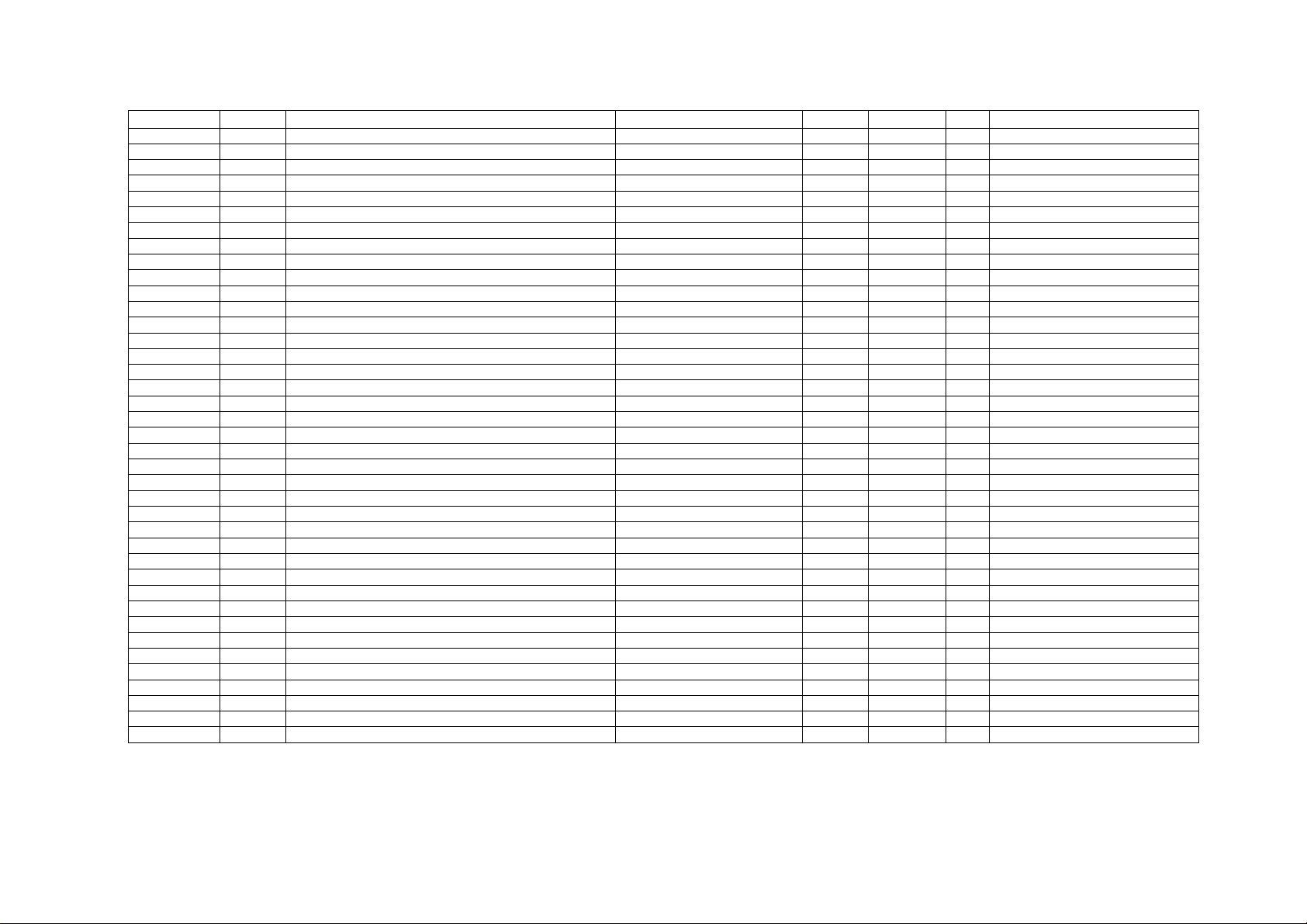
Address Point ID Description
Low and High Scales
+10 0x6E8A V3 interharmonics THD 0-999.9 0.1% UINT16 R
3
Units3
Type R/W Notes
2
+11 0x6E8B Not used 0 UINT16 R
+12 0x6E6E I1 interharmonics THD 0-999.9 0.1% UINT16 R
+13 0x6E8D I2 interharmonics THD 0-999.9 0.1% UINT16 R
+14 0x6E8E I3 interharmonics THD 0-999.9 0.1% UINT16 R
+15 0x6E8F I4 interharmonics THD 0-999.9 0.1% UINT16 R
+16 0x6E90 I1 TDD 0-100.0 0.1% UINT16 R
+17 0x6E91 I2 TDD 0-100.0 0.1% UINT16 R
+18 0x6E92 I3 TDD 0-100.0 0.1% UINT16 R
+19 0x6E93 I4 TDD 0-100.0 0.1% UINT16 R
+20 0x6E94 I1 K-Factor 1.0-999.9 0.1 UINT16 R
+21 0x6E95 I2 K-Factor 1.0-999.9 0.1 UINT16 R
+22 0x6E96 I3 K-Factor 1.0-999.9 0.1 UINT16 R
+23 0x6E97 I4 K-Factor 1.0-999.9 0.1 UINT16 R
10688-10719 10-Minute Total Harmonics
+0 0x6F00 V1 THD 0-999.9 0.1% UINT16 R 2
+1 0x6F01 V2 THD 0-999.9 0.1% UINT16 R 2
+2 0x6F02 V3 THD 0-999.9 0.1% UINT16 R 2
+3 0x6F03 Not used 0 0 UINT16 R
+4 0x6F04 I1 THD 0-999.9 0.1% UINT16 R
+5 0x6F05 I2 THD 0-999.9 0.1% UINT16 R
+6 0x6F06 I3 THD 0-999.9 0.1% UINT16 R
+7 0x6F07 I4 THD 0-999.9 0.1% UINT16 R
+8 0x6F08 V1 interharmonics THD 0-999.9 0.1% UINT16 R
+9 0x6F09 V2 interharmonics THD 0-999.9 0.1% UINT16 R
+10 0x6F0A V3 interharmonics THD 0-999.9 0.1% UINT16 R
2
2
2
+11 0x6F0B Not used 0 UINT16 R
+12 0x6F0C I1 interharmonics THD 0-999.9 0.1% UINT16 R
+13 0x6F0D I2 interharmonics THD 0-999.9 0.1% UINT16 R
+14 0x6F0E I3 interharmonics THD 0-999.9 0.1% UINT16 R
+15 0x6F0F I4 interharmonics THD 0-999.9 0.1% UINT16 R
+16 0x6F10 I1 TDD 0-100.0 0.1% UINT16 R
+17 0x6F11 I2 TDD 0-100.0 0.1% UINT16 R
+18 0x6F12 I3 TDD 0-100.0 0.1% UINT16 R
+19 0x6F13 I4 TDD 0-100.0 0.1% UINT16 R
+20 0x6F14 I1 K-Factor 1.0-999.9 0.1 UINT16 R
+21 0x6F15 I2 K-Factor 1.0-999.9 0.1 UINT16 R
+22 0x6F16 I3 K-Factor 1.0-999.9 0.1 UINT16 R
+23 0x6F17 I4 K-Factor 1.0-999.9 0.1 UINT16 R
NOTES:
1
When the 4LN3, 4LL3, 3LN3 or 3LL3 wiring mode is selected, the voltages will be line-to-neutral; for any other wiring mode, they will be line-to-line.
42

2
When the 4LN3 or 3LN3 wiring mode is selected, the voltages will be line-to-neutral; for any other wiring mode, th ey will be line-to-line voltages.
3
For volts, amps, power and frequency scales and units refer to Section 4 ”Data Scales and Units”. For analog data scaling formulas and examples, see Section 2.6.1, “16-bit Scaled Integer
Format”.
4
Harmonic angles are referenced to the fundamental voltage harmonic H01 on phase L1.
5
On a 0.2-s interval.
6
On a 3-s interval.
43

3.4 32-bit Analog Registers, Binary Registers and Counters
Address Point ID Description
11776-11777 0x0000 None 0 UINT32 R
11840 0x0080 Setpoint Status 0x00000000-0x0000FFFF UINT32 R Bitmap: 0=released, 1=operated
11904-11907 Special Inputs
+0,1 0x0100 Not used 0 UINT32 R
+2,3 0x0101 Phase rotation order 0=error, 1=positive (ABC),
12160-12161 0x0300 Event Flags 0x00000000-0x000000FF UINT32 R Bitmap: 0=OFF, 1=ON
Internal Pulsed Events 0x0400 kWh Import pulse 0/1 TRG 0x0401 kWh Export pulse 0/1 TRG 0x0402 kWh Total pulse 0/1 TRG 0x0403 kvarh Import pulse 0/1 TRG 0x0404 kvarh Export pulse 0/1 TRG 0x0405 kvarh Total pulse 0/1 TRG 0x0406 kVAh pulse 0/1 TRG 0x0407 Start of power demand interval pulse 0/1 TRG
0x0408 Start of tariff interval pulse 0/1 TRG 12544-12545 0x0600 Digital Inputs 0x00000000-0x000000FF UINT32 R Bitmap: 0=open, 1=closed 12800-12801 0x0800 Relay Outputs 0x00000000-0x0000000F UINT32 R Bitmap: 0=open, 1=closed
Internal Static Events
0x0900 Phase order error 0/1 TRG
0x0901 Positive phase order 0/1 TRG
0x0902 Negative phase order 0/1 TRG
0x0903 PQ event 0/1 TRG
0x0904 General fault event 0/1 TRG
0x0905 Fault detected 0/1 TRG
0x0906 External fault trigger 0/1 TRG
0x0907 Device fault 0/1 TRG
0x0908 No voltage 0/1 TRG 13056-13071 Counters
+0,1 0x0A00 Counter #1 0-999,999,999 UINT32 R/W
+2,3 0x0A01 Counter #2 0-999,999,999 UINT32 R/W
+4,5 0x0A02 Counter #3 0-999,999,999 UINT32 R/W
+6,7 0x0A03 Counter #4 0-999,999,999 UINT32 R/W
+8,9 0x0A04 Counter #5 0-999,999,999 UINT32 R/W
+10,11 0x0A05 Counter #6 0-999,999,999 UINT32 R/W
+12,13 0x0A06 Counter #7 0-999,999,999 UINT32 R/W
+14,15 0x0A07 Counter #8 0-999,999,999 UINT32 R/W
Time/Date 0x0B00 Not used 0 UINT32 TRG
Options/Range
2=negative (CBA)
3
Units3
UINT32 R
Type R/W Notes
44

Address Point ID Description
Options/Range
3
Units3
Type R/W Notes
0x0B01 Not used 0 UINT32 TRG
0x0B02 Day of week 1-7, 1 = Sun, 7 = Sat UINT32 TRG
0x0B03 Year 0-99 UINT32 TRG
0x0B04 Month 1-12 UINT32 TRG
0x0B05 Day of month 1-31 UINT32 TRG
0x0B06 Hours 0-23 UINT32 TRG
0x0B07 Minutes 0-59 UINT32 TRG
0x0B08 Seconds 0-59 UINT32 TRG
0x0B09 Minute interval 1,2,3,4,5,10,15,20,30,60 UINT32 TRG
13248-13297 1/2-Cycle Values
+0, 1 0x0B80 V1 Voltage 0-Vmax U1 UINT32 R
+2, 3 0x0B81 V2 Voltage 0-Vmax U1 UINT32 R
+4, 5 0x0B82 V3 Voltage 0-Vmax U1 UINT32 R
1
1
1
+6, 7 0x0B83 Not used 0 UINT32 R
+8, 9 0x0B84 V12 Voltage 0-Vmax U1 UINT32 R
+10, 11 0x0B85 V23 Voltage 0-Vmax U1 UINT32 R
+12, 13 0x0B86 V31 Voltage 0-Vmax U1 UINT32 R
+14, 15 0x0B87 I1 Current 0-Imax U4 UINT32 R
+16, 17 0x0B88 I2 Current 0-Imax U4 UINT32 R
+18, 19 0x0B89 I3 Current 0-Imax U4 UINT32 R
+20, 21 0x0B8A I4 Current 0-I4max U4 UINT32 R
+22, 23 0x0B8B In Current 0-Imax U4 UINT32 R
+24, 25 0x0B8C Not used 0 UINT32 R
+26, 27 0x0B8D Not used 0 UINT32 R
+28, 29 0x0B8E Not used 0 UINT32 R
+30, 31 0x0B8F Not used 0 UINT32 R
+32, 33 0x0B90 Not used 0 UINT32 R
+34, 35 0x0B91 Zero-sequence voltage 0-Vmax U1 UINT32 R
+36, 37 0x0B92 Zero-sequence current 0-Imax U4 UINT32 R
+38, 39 0x0B93 Not used 0 UINT32 R
+40, 41 0x0B94 Voltage unbalance 0-3000
+42, 43 0x0B95 Current unbalance 0-3000
×0.1%
×0.1%
UINT32 R
UINT32 R
+44, 45 0x0B96 Not used 0 UINT32 R
+46, 47 0x0B97 Not used 0 UINT32 R
+48, 49 0x0B98 Frequency (1-cycle) 0-10000
×0.01Hz
UINT32 R
13312-13377 1-Cycle Phase Values
+0,1 0x0C00 V1/V12 Voltage 0-Vmax U1 UINT32 R 1
+2,3 0x0C01 V2/V23 Voltage 0-Vmax U1 UINT32 R 1
+4,5 0x0C02 V3/V31 Voltage 0-Vmax U1 UINT32 R 1
+6,7 0x0C03 I1 Current 0-Imax U4 UINT32 R
+8,9 0x0C04 I2 Current 0-Imax U4 UINT32 R
+10,11 0x0C05 I3 Current 0-Imax U4 UINT32 R
+12,13 0x0C06 kW L1 -Pmax-Pmax U3 INT32 R
45

Address Point ID Description
Options/Range
3
Units3
Type R/W Notes
+14,15 0x0C07 kW L2 -Pmax-Pmax U3 INT32 R
+16,17 0x0C08 kW L3 -Pmax-Pmax U3 INT32 R
+18,19 0x0C09 kvar L1 -Pmax-Pmax U3 INT32 R
+20,21 0x0C0A kvar L2 -Pmax-Pmax U3 INT32 R
+22,23 0x0C0B kvar L3 -Pmax-Pmax U3 INT32 R
+24,25 0x0C0C kVA L1 0-Pmax U3 UINT32 R
+26,27 0x0C0D kVA L2 0-Pmax U3 UINT32 R
+28,29 0x0C0E kVA L3 0-Pmax U3 UINT32 R
+30,31 0x0C0F Power factor L1 -1000-1000
+32,33 0x0C10 Power factor L2 -1000-1000
+34,35 0x0C11 Power factor L3 -1000-1000
+36,37 0x0C12 V1/V12 Voltage THD 0-9999
+38,39 0x0C13 V2/V23 Voltage THD 0-9999
+40,41 0x0C14 V3/V31 Voltage THD 0-9999
+42,43 0x0C15 I1 Current THD 0-9999
+44,45 0x0C16 I2 Current THD 0-9999
+46,47 0x0C17 I3 Current THD 0-9999
+48,49 0x0C18 I1 K-Factor 10-9999
+50,51 0x0C19 I2 K-Factor 10-9999
+52,53 0x0C1A I3 K-Factor 10-9999
+54,55 0x0C1B I1 Current TDD 0-1000
+56,57 0x0C1C I2 Current TDD 0-1000
+58,59 0x0C1D I3 Current TDD 0-1000
×0.001
×0.001
×0.001
×0.1%
×0.1%
×0.1%
×0.1%
×0.1%
×0.1%
×0.1
×0.1
×0.1
×0.1%
×0.1%
×0.1%
INT32 R
INT32 R
INT32 R
UINT32 R
UINT32 R
UINT32 R
2, 5
2, 5
2, 5
UINT32 R 5
UINT32 R 5
UINT32 R 5
UINT32 R 5
UINT32 R 5
UINT32 R 5
UINT32 R 5
UINT32 R 5
UINT32 R 5
+60,61 0x0C1E V12 Voltage 0-Vmax U1 UINT32 R
+62,63 0x0C1F V23 Voltage 0-Vmax U1 UINT32 R
+64,65 0x0C20 V31 Voltage 0-Vmax U1 UINT32 R
13440-13463 1-Cycle Low Phase Values
+0,1 0x0D00 Low voltage 0-Vmax U1 UINT32 R 1
+2,3 0x0D01 Low current 0-Imax U4 UINT32 R
+4,5 0x0D02 Low kW -Pmax-Pmax U3 INT32 R
+6,7 0x0D03 Low kvar -Pmax-Pmax U3 INT32 R
+8,9 0x0D04 Low kVA 0-Pmax U3 UINT32 R
+10,11 0x0D05 Low PF Lag 0-1000
+12,13 0x0D06 Low PF Lead 0-1000
+14,15 0x0D07 Low voltage THD 0-9999
+16,17 0x0D08 Low current THD 0-9999
+18,19 0x0D09 Low K-Factor 10-9999
+20,21 0x0D0A Low current TDD 0-1000
×0.001
×0.001
×0.1%
×0.1%
×0.1
×0.1%
UINT32 R
UINT32 R
UINT32 R
2, 5
UINT32 R 5
UINT32 R 5
UINT32 R 5
+22,23 0x0D0B Low L-L voltage 0-Vmax U1 UINT32 R 5
13568-13591 1-Cycle High Phase Values
+0,1 0x0E00 High voltage 0-Vmax U1 UINT32 R 1
+2,3 0x0E01 High current 0-Imax U4 UINT32 R
+4,5 0x0E02 High kW -Pmax-Pmax U3 INT32 R
46

Address Point ID Description
Options/Range
3
Units3
Type R/W Notes
+6,7 0x0E03 High kvar -Pmax-Pmax U3 INT32 R
+8,9 0x0E04 High kVA 0-Pmax U3 UINT32 R
+10,11 0x0E05 High PF Lag 0-1000
+12,13 0x0E06 High PF Lead 0-1000
+14,15 0x0E07 High voltage THD 0-9999
+16,17 0x0E08 High current THD 0-9999
+18,19 0x0E09 High K-Factor 10-9999
+20,21 0x0E0A High current TDD 0-1000
×0.001
×0.001
×0.1%
×0.1%
×0.1
×0.1%
+22,23 0x0E0B High L-L voltage 0-Vmax U1 UINT32 R
UINT32 R
UINT32 R
UINT32 R
2, 5
UINT32 R 5
UINT32 R 5
UINT32 R 5
5
13696-13721 1-Cycle Total Values
+0,1 0x0F00 Total kW -Pmax-Pmax U3 INT32 R
+2,3 0x0F01 Total kvar -Pmax-Pmax U3 INT32 R
+4,5 0x0F02 Total kVA 0-Pmax U3 UINT32 R
+6,7 0x0F03 Total PF -1000-1000
+8,9 0x0F04 Total PF lag 0-1.000
+10,11 0x0F05 Total PF lead 0-1.000
×0.001
×0.001
×0.001
INT32 R
UINT16 R
UINT16 R
+12,13 0x0F06 Total kW import 0-Pmax U3 UINT32 R
+14,15 0x0F07 Total kW export 0-Pmax U3 UINT32 R
+16,17 0x0F08 Total kvar import 0-Pmax U3 UINT32 R
+18,19 0x0F09 Total kvar export 0-Pmax U3 UINT32 R
+20,21 0x0F0A 3-phase average L-N/L-L voltage 0-Vmax U1 UINT32 R
1
+22,23 0x0F0B 3-phase average L-L voltage 0-Vmax U1 UINT32 R
+24,25 0x0F0C 3-phase average current 0-Imax U2 UINT32 R
13824-13837 1-Cycle Auxiliary Values
+0,1 0x1000 I4 current 0-I4max U4 UINT32 R
+2,3 0x1001 In (neutral) Current 0-Imax U4 UINT32 R
+4,5 0x1002 Frequency 0-Fmax
+6,7 0x1003 Voltage unbalance 0-3000
+8,9 0x1004 Current unbalance 0-3000
×0.01Hz
×0.1%
×0.1%
UINT32 R
UINT32 R
UINT32 R
+10,11 0x1005 Not used 0 UINT32 R
+12,13 0x1006 Not used 0 UINT32 R
13888-13919 Phasor
+0,1 0x1080 V1/V12 Voltage magnitude 0-Vmax U1 UINT32 R
+2,3 0x1081 V2/V23 Voltage magnitude 0-Vmax U1 UINT32 R
+4,5 0x1082 V3/V31 Voltage magnitude 0-Vmax U1 UINT32 R
2
2
2
+6,7 0x1083 Not used UINT32 R
+8,9 0x1084 I1 Current magnitude 0-Imax U4 UINT32 R
+10,11 0x1085 I2 Current magnitude 0-Imax U4 UINT32 R
+12,13 0x1086 I3 Current magnitude 0-Imax U4 UINT32 R
+14,15 0x1087 I4 Current magnitude 0-I4max U4 UINT32 R
+16,17 0x1088 V1/V12 Voltage angle -1800-1800
+18,19 0x1089 V2/V23 Voltage angle -1800-1800
+20,21 0x108A V3/V31 Voltage angle -1800-1800
×0.1º
×0.1º
×0.1º
INT32 R 2
INT32 R 2
INT32 R 2
47

Address Point ID Description
Options/Range
3
Units3
Type R/W Notes
+22,23 0x108B Not used INT32 R
+24,25 0x108C I1 Current angle -1800-1800
+26,27 0x108D I2 Current angle -1800-1800
+28,29 0x108E I3 Current angle -1800-1800
+30,31 0x108F I4 Current angle -1800-1800
×0.1º
×0.1º
×0.1º
×0.1º
INT32 R
INT32 R
INT32 R
INT32 R
13952-14029 1-Second Phase Values
+0,1 0x1100 V1/V12 Voltage 0-Vmax U1 UINT32 R 1
+2,3 0x1101 V2/V23 Voltage 0-Vmax U1 UINT32 R 1
+4,5 0x1102 V3/V31 Voltage 0-Vmax U1 UINT32 R 1
+6,7 0x1103 I1 Current 0-Imax U2 UINT32 R
+8,9 0x1104 I2 Current 0-Imax U2 UINT32 R
+10,11 0x1105 I3 Current 0-Imax U2 UINT32 R
+12,13 0x1106 kW L1 -Pmax-Pmax U3 INT32 R
+14,15 0x1107 kW L2 -Pmax-Pmax U3 INT32 R
+16,17 0x1108 kW L3 -Pmax-Pmax U3 INT32 R
+18,19 0x1109 kvar L1 -Pmax-Pmax U3 INT32 R
+20,21 0x110A kvar L2 -Pmax-Pmax U3 INT32 R
+22,23 0x110B kvar L3 -Pmax-Pmax U3 INT32 R
+24,25 0x110C kVA L1 0-Pmax U3 UINT32 R
+26,27 0x110D kVA L2 0-Pmax U3 UINT32 R
+28,29 0x110E kVA L3 0-Pmax U3 UINT32 R
+30,31 0x110F Power factor L1 -1000-1000
+32,33 0x1110 Power factor L2 -1000-1000
+34,35 0x1111 Power factor L3 -1000-1000
+36,37 0x1112 V1/V12 Voltage THD 0-9999
+38,39 0x1113 V2/V23 Voltage THD 0-9999
+40,41 0x1114 V3/V31 Voltage THD 0-9999
+42,43 0x1115 I1 Current THD 0-9999
+44,45 0x1116 I2 Current THD 0-9999
+46,47 0x1117 I3 Current THD 0-9999
+48,49 0x1118 I1 K-Factor 10-9999
+50,51 0x1119 I2 K-Factor 10-9999
+52,53 0x111A I3 K-Factor 10-9999
+54,55 0x111B I1 Current TDD 0-1000
+56,57 0x111C I2 Current TDD 0-1000
+58,59 0x111D I3 Current TDD 0-1000
×0.001
×0.001
×0.001
×0.1%
×0.1%
×0.1%
×0.1%
×0.1%
×0.1%
×0.1
×0.1
×0.1
×0.1%
×0.1%
×0.1%
INT32 R
INT32 R
INT32 R
UINT32 R
UINT32 R
UINT32 R
2, 6
2, 6
2, 6
UINT32 R 6
UINT32 R 6
UINT32 R 6
UINT32 R 6
UINT32 R 6
UINT32 R 6
UINT32 R 6
UINT32 R 6
UINT32 R 6
+60,61 0x111E V12 Voltage 0-Vmax U1 UINT32 R
+62,63 0x111F V23 Voltage 0-Vmax U1 UINT32 R
+64,65 0x1120 V31 Voltage 0-Vmax U1 UINT32 R
+66,67 0x1121 Not used 0 UINT32 R
+68,69 0x1122 Not used 0 UINT32 R
+70,71 0x1123 Not used 0 UINT32 R
+72,73 0x1124 V1x Voltage 0-Vmax U1 UINT32 R Transient recorder V1 channel
48

Address Point ID Description
Options/Range
3
Units3
Type R/W Notes
+74,75 0x1125 V2x Voltage 0-Vmax U1 UINT32 R Transient recorder V2 channel
+76,77 0x1126 V3x Voltage 0-Vmax U1 UINT32 R Transient recorder V3 channel
14080-14103 1-Second Low Phase Values
+0,1 0x1200 Low voltage 0-Vmax U1 UINT32 R 1
+2,3 0x1201 Low current 0-Imax U2 UINT32 R
+4,5 0x1202 Low kW -Pmax-Pmax U3 INT32 R
+6,7 0x1203 Low kvar -Pmax-Pmax U3 INT32 R
+8,9 0x1204 Low kVA 0-Pmax U3 UINT32 R
+10,11 0x1205 Low PF Lag 0-1000
+12,13 0x1206 Low PF Lead 0-1000
+14,15 0x1207 Low voltage THD 0-9999
+16,17 0x1208 Low current THD 0-9999
+18,19 0x1209 Low K-Factor 10-9999
+20,21 0x120A Low current TDD 0-1000
×0.001
×0.001
×0.1%
×0.1%
×0.1
×0.1%
UINT32 R
UINT32 R
UINT32 R
2, 6
UINT32 R 6
UINT32 R 6
UINT32 R 6
+22,23 0x120B Low L-L voltage 0-Vmax U1 UINT32 R
14144-14175 3-Second Powers
+0,1 0x1280 kW L1 -Pmax-Pmax U3 INT32 R
+2,3 0x1281 kW L2 -Pmax-Pmax U3 INT32 R
+4,5 0x1282 kW L3 -Pmax-Pmax U3 INT32 R
+6,7 0x1283 kvar L1 -Pmax-Pmax U3 INT32 R
+8,9 0x1284 kvar L2 -Pmax-Pmax U3 INT32 R
+10,11 0x1285 kvar L3 -Pmax-Pmax U3 INT32 R
+12,13 0x1286 kVA L1 0-Pmax U3 UINT32 R
+14,15 0x1287 kVA L2 0-Pmax U3 UINT32 R
+16,17 0x1288 kVA L3 0-Pmax U3 UINT32 R
+18,19 0x1289 Power factor L1 -1000-1000
+20,21 0x128A Power factor L2 -1000-1000
+22,23 0x128B Power factor L3 -1000-1000
×0.001
×0.001
×0.001
INT32 R
INT32 R
INT32 R
+24,25 0x128C Total kW -Pmax-Pmax U3 INT32 R
+26,27 0x128D Total kvar -Pmax-Pmax U3 INT32 R
+28,29 0x128E Total kVA 0-Pmax U3 UINT32 R
+30,31 0x128F Total PF -1000-1000
×0.001
INT32 R
14208-14231 1-Second High Phase Values
+0,1 0x1300 High voltage 0-Vmax U1 UINT32 R 1
+2,3 0x1301 High current 0-Imax U2 UINT32 R
+4,5 0x1302 High kW -Pmax-Pmax U3 INT32 R
+6,7 0x1303 High kvar -Pmax-Pmax U3 INT32 R
+8,9 0x1304 High kVA 0-Pmax U3 UINT32 R
+10,11 0x1305 High PF Lag 0-1000
+12,13 0x1306 High PF Lead 0-1000
+14,15 0x1307 High voltage THD 0-9999
+16,17 0x1308 High current THD 0-9999
+18,19 0x1309 High K-Factor 10-9999
×0.001
×0.001
×0.1%
×0.1%
×0.1
UINT32 R
UINT32 R
UINT32 R
2, 6
UINT32 R 6
UINT32 R 6
49

Address Point ID Description
+20,21 0x130A High current TDD 0-1000
Options/Range
3
Units3
×0.1%
Type R/W Notes
UINT32 R 6
+22,23 0x130B High L-L voltage 0-Vmax U1 UINT32 R
14336-14379 1-Second Total Values
+0,1 0x1400 Total kW -Pmax-Pmax U3 INT32 R
+2,3 0x1401 Total kvar -Pmax-Pmax U3 INT32 R
+4,5 0x1402 Total kVA 0-Pmax U3 UINT32 R
+6,7 0x1403 Total PF -1000-1000
+8,9 0x1404 Total PF lag 0-1.000
+10,11 0x1405 Total PF lead 0-1.000
×0.001
×0.001
×0.001
INT32 R
UINT16 R
UINT16 R
+12,13 0x1406 Total kW import 0-Pmax U3 UINT32 R
+14,15 0x1407 Total kW export 0-Pmax U3 UINT32 R
+16,17 0x1408 Total kvar import 0-Pmax U3 UINT32 R
+18,19 0x1409 Total kvar export 0-Pmax U3 UINT32 R
+20,21 0x140A 3-phase average L-N/L-L voltage 0-Vmax U1 UINT32 R
1
+22,23 0x140B 3-phase average L-L voltage 0-Vmax U1 UINT32 R
+24,25 0x140C 3-phase average current 0-Imax U2 UINT32 R
+26,27 0x140D Not used 0 UINT32 R
+28,29 0x140E Total kW Fe losses -Pmax-Pmax U3 INT32 R
+30,31 0x140F Total kW Cu losses -Pmax-Pmax U3 INT32 R
+32,33 0x1410 Total kvar Fe losses -Pmax-Pmax U3 INT32 R
+34,35 0x1411 Total kvar Cu losses -Pmax-Pmax U3 INT32 R
+36,37 0x1412 Total uncompensated kW -Pmax-Pmax U3 INT32 R
+38,39 0x1413 Total uncompensated kvar -Pmax-Pmax U3 INT32 R
+40,41 0x1414 Total uncompensated kVA 0-Pmax U3 UINT32 R
+42,43 0x1415 Total uncompensated PF -1000-1000
×0.001
INT32 R
14400-14409 Uncompensated Total Energy
+0,1 0x1480 kWh uncompensated import 0-999,999,999 0.1 kWh UINT32 R
+2,3 0x1481 kWh uncompensated export 0-999,999,999 0.1 kWh UINT32 R
+4,5 0x1482 kvarh uncompensated import 0-999,999,999 0.1 kvarh UINT32 R
+6,7 0x1483 kvarh uncompensated export 0-999,999,999 0.1 kvarh UINT32 R
+8,9 0x1484 kVAh uncompensated total 0-999,999,999 0.1 kVAh UINT32 R
14464-14483 1-Second Auxiliary Values
+0,1 0x1500 I4 current 0-I4max U4 UINT32 R
+2,3 0x1501 In (neutral) Current 0-Imax U4 UINT32 R
+4,5 0x1502 Frequency 0-Fmax
+6,7 0x1503 Voltage unbalance 0-3000
+8,9 0x1504 Current unbalance 0-3000
+10,11 0x1505 Battery DC voltage 0-999900
×0.01Hz
×0.1%
×0.1%
×0.01V
UINT32 R
UINT32 R
UINT32 R
UINT32 R
+12,13 0x1506 Not used 0 UINT32 R
+14,15 0x1507 Not used 0 UINT32 R
+16,17 0x1508 V4x (neutral-ground) voltage 0-Vmax U1 UINT32 R Transient recorder Vn channel
+18,19 0x1509 Internal temperature -2000 to 2000
×0.1ºC
INT32 R
50

Address Point ID Description
Options/Range
3
Units3
Type R/W Notes
14528-14551 Present Harmonic Demands
+0,1 0x1580 V1/V12 THD demand 0-9999
+2,3 0x1581 V2/V23 THD demand 0-9999
+4,5 0x1582 V3/V31 THD demand 0-9999
×0.1%
×0.1%
×0.1%
UINT32 R 2
UINT32 R 2
UINT32 R 2
+6,7 0x1583 Not used 0 UINT32 R
+8,9 0x1584 I1 THD demand 0-9999
+10,11 0x1585 I2 THD demand 0-9999
+12,13 0x1586 I3 THD demand 0-9999
+14,15 0x1587 I4 THD demand 0-9999
+16,17 0x1588 I1 TDD demand 0-1000
+18,19 0x1589 I2 TDD demand 0-1000
+20,21 0x158A I3 TDD demand 0-1000
+22,23 0x158B I4 TDD demand 0-1000
×0.1%
×0.1%
×0.1%
×0.1%
×0.1%
×0.1%
×0.1%
×0.1%
UINT32 R
UINT32 R
UINT32 R
UINT32 R
UINT32 R
UINT32 R
UINT32 R
UINT32 R
14592-14659 Present Demands
+0,1 0x1600 V1/V12 Volt demand 0-Vmax U1 UINT32 R
+2,3 0x1601 V2/V23 Volt demand 0-Vmax U1 UINT32 R
+4,5 0x1602 V3/V31 Volt demand 0-Vmax U1 UINT32 R
2
2
2
+6,7 0x1603 I1 Ampere demand 0-Imax U2 UINT32 R
+8,9 0x1604 I2 Ampere demand 0-Imax U2 UINT32 R
+10,11 0x1605 I3 Ampere demand 0-Imax U2 UINT32 R
+12,13 0x1606 kW import block demand 0-Pmax U3 UINT32 R
+14,15 0x1607 kvar import block demand 0-Pmax U3 UINT32 R
+16,17 0x1608 kVA block demand 0-Pmax U3 UINT32 R
+18,19 0x1609 kW import sliding window demand 0-Pmax U3 UINT32 R
+20,21 0x160A kvar import sliding window demand 0-Pmax U3 UINT32 R
+22,23 0x160B kVA sliding window demand 0-Pmax U3 UINT32 R
+24,25 0x160C Not used 0 UINT32 R
+26,27 0x160D Not used 0 UINT32 R
+28,29 0x160E Not used 0 UINT32 R
+30,31 0x160F kW import accumulated demand 0-Pmax U3 UINT32 R
+32,33 0x1610 kvar import accumulated demand 0-Pmax U3 UINT32 R
+34,35 0x1611 kVA accumulated demand 0-Pmax U3 UINT32 R
+36,37 0x1612 kW import predicted sliding window demand 0-Pmax U3 UINT32 R
+38,39 0x1613 kvar import predicted sliding window demand 0-Pmax U3 UINT32 R
+40,41 0x1614 kVA predicted sliding window demand 0-Pmax U3 UINT32 R
+42,43 0x1615 PF (import) at Max. kVA sliding window demand 0-1000
×0.001
UINT32 R
+44,45 0x1616 kW export block demand 0-Pmax U3 UINT32 R
+46,47 0x1617 kvar export block demand 0-Pmax U3 UINT32 R
+48,49 0x1618 kW export sliding window demand 0-Pmax U3 UINT32 R
+50,51 0x1619 kvar export sliding window demand 0-Pmax U3 UINT32 R
+52,53 0x161A kW export accumulated demand 0-Pmax U3 UINT32 R
+54,55 0x161B kvar export accumulated demand 0-Pmax U3 UINT32 R
+56,57 0x161C kW export predicted sliding window demand 0-Pmax U3 UINT32 R
51

Address Point ID Description
+58,59 0x161D kvar export predicted sliding window demand 0-Pmax U3 UINT32 R
+60,61 0x161E Not used 0 UINT32 R
+62,63 0x161F Not used 0 UINT32 R
+64,65 0x1620 Not used 0 UINT32 R
+66,67 0x1621 I4 ampere demand 0-I4max U4 UINT32 R
14720-14737 Instrumentation To tal Energies
+0,1 0x1700 kWh import 0-999,999,999 0.1 kWh UINT32 R
+2,3 0x1701 kWh export 0-999,999,999 0.1 kWh UINT32 R
+4,5 0x1702 kWh net -999,999,999-999,999,999 0.1 kWh INT32 R
+6,7 0x1703 Not used 0 UINT32 R
+8,9 0x1704 kvarh import 0-999,999,999 0.1 kvarh UINT32 R
+10,11 0x1705 kvarh export 0-999,999,999 0.1 kvarh UINT32 R
+12,13 0x1706 kvarh net -999,999,999-999,999,999 0.1 kvarh INT32 R
+14,15 0x1707 Not used 0 UINT32 R
+16,17 0x1708 kVAh total 0-999,999,999 0.1 kVAh UINT32 R
+18,19 0x1709 Not used UINT32 R
+20,21 0x170A Not used UINT32 R
+22,23 0x170B kVAh import 0-999,999,999 0.1 kVAh UINT32 R
+24,25 0x170C kVAh export 0-999,999,999 0.1 kVAh UINT32 R
+26,27 0x170D Not used UINT32 R
+28,29 0x170E Not used UINT32 R
+30,31 0x170F Not used UINT32 R
+32,33 0x1710 Not used UINT32 R
+34,35 0x1711 Not used UINT32 R
+36,37 0x1712 kvarh Q1 0-999,999,999 0.1 kvarh UINT32 R
+38,39 0x1713 kvarh Q2 0-999,999,999 0.1 kvarh UINT32 R
+40,41 0x1714 kvarh Q3 0-999,999,999 0.1 kvarh UINT32 R
+42,43 0x1715 kvarh Q4 0-999,999,999 0.1 kvarh UINT32 R
14784-14803 Billing Summary (Total) Energy Registers
+0,1 0x1780 Summary energy register #1 0-999,999,999 0.1 kWh UINT32 R
+2,3 0x1781 Summary energy register #2 0-999,999,999 0.1 kWh UINT32 R
…
+18,19 0x1789 Summary energy register #10 0-999,999,999 0.1 kWh UINT32 R
14912-14931 Symmetrical Components
+0,1 0x1880 Positive-sequence voltage 0-Vmax U1 UINT32 R
+2,3 0x1881 Negative-sequence voltage 0-Vmax U1 UINT32 R
+4,5 0x1882 Zero-sequence voltage 0-Vmax U1 UINT32 R
+6,7 0x1883 Negative-sequence voltage unbalance 0-3000
+8,9 0x1884 Zero-sequence voltage unbalance 0-3000
+10,11 0x1885 Positive-sequence current 0-Imax U4 UINT32 R
+12,13 0x1886 Negative-sequence current 0-Imax U4 UINT32 R
+14,15 0x1887 Zero-sequence current 0-Imax U4 UINT32 R
+16,17 0x1888 Negative-sequence current unbalance 0-3000
Options/Range
3
Units3
×0.1%
×0.1%
×0.1%
Type R/W Notes
UINT32 R
UINT32 R
UINT32 R
52

Address Point ID Description
Options/Range
+18,19 0x1889 Zero-sequence current unbalance 0-3000
14976-15075 V1/V12 Harmonic Distortion
+0,1 0x1900 H01 Harmonic distortion 0-10000
+2,3 0x1901 H02 Harmonic distortion 0-10000
3
Units3
×0.1%
×0.01%
×0.01%
Type R/W Notes
UINT32 R
2
UINT32 R
UINT32 R
...
+98,99 0x1931 H50 Harmonic distortion 0-10000
×0.01%
15104-15203 V2/V23 Harmonic Distortion
+0,1 0x1A00 H01 Harmonic distortion 0-10000
+2,3 0x1A01 H02 Harmonic distortion 0-10000
×0.01%
×0.01%
UINT32 R
2
UINT32 R
UINT32 R
...
+98,99 0x1A31 H50 Harmonic distortion 0-10000
×0.01%
15232-15331 V3/V31 Harmonic Distortion
+0,1 0x1B00 H01 Harmonic distortion 0-10000
+2,3 0x1B01 H02 Harmonic distortion 0-10000
×0.01%
×0.01%
UINT32 R
2
UINT32 R
UINT32 R
...
+98,99 0x1B31 H50 Harmonic distortion 0-10000
×0.01%
UINT32 R
15360-15459 I1 Harmonic Distortion
+0,1 0x1C00 H01 Harmonic distortion 0-10000
+2,3 0x1C01 H02 Harmonic distortion 0-10000
×0.01%
×0.01%
UINT32 R
UINT32 R
...
+98,99 0x1C31 H50 Harmonic distortion 0-10000
×0.01%
UINT32 R
15488-15587 I2 Harmonic Distortion
+0,1 0x1D00 H01 Harmonic distortion 0-10000
+2,3 0x1D01 H02 Harmonic distortion 0-10000
×0.01%
×0.01%
UINT32 R
UINT32 R
...
+98,99 0x1D31 H50 Harmonic distortion 0-10000
×0.01%
UINT32 R
15616-15715 I3 Harmonic Distortion
+0,1 0x1E00 H01 Harmonic distortion 0-10000
+2,3 0x1E01 H02 Harmonic distortion 0-10000
×0.01%
×0.01%
UINT32 R
UINT32 R
...
+98,99 0x1E31 H50 Harmonic distortion 0-10000
×0.01%
UINT32 R
17280-17379 I4 Harmonic Distortion
+0,1 0x2B00 H01 Harmonic distortion 0-10000
+2,3 0x2B01 H02 Harmonic distortion 0-10000
×0.01%
×0.01%
UINT32 R
UINT32 R
...
+98,99 0x2B31 H50 Harmonic distortion 0-10000
×0.01%
17024-17059 Fundamental Phase Values
UINT32 R
5
+0,1 0x2900 V1/V12 Voltage 0-Vmax U1 UINT32 R 2
+2,3 0x2901 V2/V23 Voltage 0-Vmax U1 UINT32 R 2
+4,5 0x2902 V3/V31 Voltage 0-Vmax U1 UINT32 R 2
+6,7 0x2903 I1 Current 0-Imax U4 UINT32 R
+8,9 0x2904 I2 Current 0-Imax U4 UINT32 R
+10,11 0x2905 I3 Current 0-Imax U4 UINT32 R
53

Address Point ID Description
Options/Range
3
Units3
Type R/W Notes
+12,13 0x2906 kW L1 -Pmax-Pmax U3 INT32 R
+14,15 0x2907 kW L2 -Pmax-Pmax U3 INT32 R
+16,17 0x2908 kW L3 -Pmax-Pmax U3 INT32 R
+18,19 0x2909 kvar L1 -Pmax-Pmax U3 INT32 R
+20,21 0x290A kvar L2 -Pmax-Pmax U3 INT32 R
+22,23 0x290B kvar L3 -Pmax-Pmax U3 INT32 R
+24,25 0x290C kVA L1 0-Pmax U3 UINT32 R
+26,27 0x290D kVA L2 0-Pmax U3 UINT32 R
+28,29 0x290E kVA L3 0-Pmax U3 UINT32 R
+30,31 0x290F Power factor L1 -1000-1000
+32,33 0x2910 Power factor L2 -1000-1000
+34,35 0x2911 Power factor L3 -1000-1000
×0.001
×0.001
×0.001
INT32 R
INT32 R
INT32 R
17088-17099 Flicker 2
+0,1 0x2980 V1 Pst 0-10000
+2,3 0x2981 V2 Pst 0-10000
+4,5 0x2982 V3 Pst 0-10000
+6,7 0x2983 V1 Plt 0-10000
+8,9 0x2984 V2 Plt 0-10000
+10,11 0x2985 V3 Plt 0-10000
×0.01
×0.01
×0.01
×0.01
×0.01
×0.01
17152-17159 Fundamental Total Values
UINT32 R
UINT32 R
UINT32 R
UINT32 R
UINT32 R
UINT32 R
5
+0,1 0x2A00 Total fundamental kW -Pmax-Pmax U3 INT32 R
+2,3 0x2A01 Total fundamental kvar -Pmax-Pmax U3 INT32 R
+4,5 0x2A02 Total fundamental kVA 0-Pmax U3 UINT32 R
+6,7 0x2A03 Total fundamental PF -1000-1000
×0.001
INT32 R
17408-17473 Minimum 1-Cycle Phase Values
+0,1 0x2C00 V1/V12 Voltage 0-Vmax U1 UINT32 R 1
+2,3 0x2C01 V2/V23 Voltage 0-Vmax U1 UINT32 R 1
+4,5 0x2C02 V3/V31 Voltage 0-Vmax U1 UINT32 R 1
+6,7 0x2C03 I1 Current 0-Imax U4 UINT32 R
+8,9 0x2C04 I2 Current 0-Imax U4 UINT32 R
+10,11 0x2C05 I3 Current 0-Imax U4 UINT32 R
+12,13 0x2C06 kW L1 -Pmax-Pmax U3 INT32 R
+14,15 0x2C07 kW L2 -Pmax-Pmax U3 INT32 R
+16,17 0x2C08 kW L3 -Pmax-Pmax U3 INT32 R
+18,19 0x2C09 kvar L1 -Pmax-Pmax U3 INT32 R
+20,21 0x2C0A kvar L2 -Pmax-Pmax U3 INT32 R
+22,23 0x2C0B kvar L3 -Pmax-Pmax U3 INT32 R
+24,25 0x2C0C kVA L1 0-Pmax U3 UINT32 R
+26,27 0x2C0D kVA L2 0-Pmax U3 UINT32 R
+28,29 0x2C0E kVA L3 0-Pmax U3 UINT32 R
+30,31 0x2C0F Power factor L1 0-1000
+32,33 0x2C10 Power factor L2 0-1000
+34,35 0x2C11 Power factor L3 0-1000
×0.001
×0.001
×0.001
UINT32 R Absolute value
UINT32 R Absolute value
UINT32 R Absolute value
54

Address Point ID Description
+36,37 0x2C12 V1/V12 Voltage THD 0-9999
+38,39 0x2C13 V2/V23 Voltage THD 0-9999
+40,41 0x2C14 V3/V31 Voltage THD 0-9999
+42,43 0x2C15 I1 Current THD 0-9999
+44,45 0x2C16 I2 Current THD 0-9999
+46,47 0x2C17 I3 Current THD 0-9999
+48,49 0x2C18 I1 K-Factor 10-9999
+50,51 0x2C19 I2 K-Factor 10-9999
+52,53 0x2C1A I3 K-Factor 10-9999
+54,55 0x2C1B I1 Current TDD 0-1000
+56,57 0x2C1C I2 Current TDD 0-1000
+58,59 0x2C1D I3 Current TDD 0-1000
Options/Range
3
Units3
×0.1%
×0.1%
×0.1%
×0.1%
×0.1%
×0.1%
×0.1
×0.1
×0.1
×0.1%
×0.1%
×0.1%
Type R/W Notes
UINT32 R
UINT32 R
UINT32 R
2, 5
2, 5
2, 5
UINT32 R 5
UINT32 R 5
UINT32 R 5
UINT32 R 5
UINT32 R 5
UINT32 R 5
UINT32 R 5
UINT32 R 5
UINT32 R 5
+60,61 0x2C1E V12 voltage 0-Vmax U1 UINT32 R
+62,63 0x2C1F V23 voltage 0-Vmax U1 UINT32 R
+64,65 0x2C20 V31 voltage 0-Vmax U1 UINT32 R
17536-17547 Minimum 1-Cycle Total Values
+0,1 0x2D00 Total kW -Pmax-Pmax U3 INT32 R
+2,3 0x2D01 Total kvar -Pmax-Pmax U3 INT32 R
+4,5 0x2D02 Total kVA 0-Pmax U3 UINT32 R
+6,7 0x2D03 Total PF 0-1000
+8,9 0x2D04 Total PF lag 0-1000
+10,11 0x2D05 Total PF lead 0-1000
×0.001
×0.001
×0.001
UINT32 R Absolute value
UINT32 R
UINT32 R
17664-17673 Minimum 1-Cycle Auxiliary Values
+0,1 0x2E00 I4 current 0-I4max U4 UINT32 R
+2,3 0x2E01 In Current 0-Imax U4 UINT32 R
+4,5 0x2E02 Frequency 0-Fmax
+6,7 0x2E03 Voltage unbalance 0-3000
+8,9 0x2E04 Current unbalance 0-3000
×0.01Hz
×0.1%
×0.1%
UINT32 R
UINT32 R
UINT32 R
18432-18497 Maximum 1-Cycle Phase Values
+0,1 0x3400 V1/V12 Voltage 0-Vmax U1 UINT32 R 1
+2,3 0x3401 V2/V23 Voltage 0-Vmax U1 UINT32 R 1
+4,5 0x3402 V3/V31 Voltage 0-Vmax U1 UINT32 R 1
+6,7 0x3403 I1 Current 0-Imax U4 UINT32 R
+8,9 0x3404 I2 Current 0-Imax U4 UINT32 R
+10,11 0x3405 I3 Current 0-Imax U4 UINT32 R
+12,13 0x3406 kW L1 -Pmax-Pmax U3 INT32 R
+14,15 0x3407 kW L2 -Pmax-Pmax U3 INT32 R
+16,17 0x3408 kW L3 -Pmax-Pmax U3 INT32 R
+18,19 0x3409 kvar L1 -Pmax-Pmax U3 INT32 R
+20,21 0x340A kvar L2 -Pmax-Pmax U3 INT32 R
+22,23 0x340B kvar L3 -Pmax-Pmax U3 INT32 R
+24,25 0x340C kVA L1 0-Pmax U3 UINT32 R
+26,27 0x340D kVA L2 0-Pmax U3 UINT32 R
55

Address Point ID Description
Options/Range
3
Units3
Type R/W Notes
+28,29 0x340E kVA L3 0-Pmax U3 UINT32 R
+30,31 0x340F Power factor L1 0-1000
+32,33 0x3410 Power factor L2 0-1000
+34,35 0x3411 Power factor L3 0-1000
+36,37 0x3412 V1/V12 Voltage THD 0-9999
+38,39 0x3413 V2/V23 Voltage THD 0-9999
+40,41 0x3414 V3/V31 Voltage THD 0-9999
+42,43 0x3415 I1 Current THD 0-9999
+44,45 0x3416 I2 Current THD 0-9999
+46,47 0x3417 I3 Current THD 0-9999
+48,49 0x3418 I1 K-Factor 10-9999
+50,51 0x3419 I2 K-Factor 10-9999
+52,53 0x341A I3 K-Factor 10-9999
+54,55 0x341B I1 Current TDD 0-1000
+56,57 0x341C I2 Current TDD 0-1000
+58,59 0x341D I3 Current TDD 0-1000
×0.001
×0.001
×0.001
×0.1%
×0.1%
×0.1%
×0.1%
×0.1%
×0.1%
×0.1
×0.1
×0.1
×0.1%
×0.1%
×0.1%
UINT32 R Absolute value
UINT32 R Absolute value
UINT32 R Absolute value
UINT32 R
UINT32 R
UINT32 R
2, 5
2, 5
2, 5
UINT32 R 5
UINT32 R 5
UINT32 R 5
UINT32 R 5
UINT32 R 5
UINT32 R 5
UINT32 R 5
UINT32 R 5
UINT32 R 5
+60,61 0x341E V12 voltage 0-Vmax U1 UINT32 R
+62,63 0x341F V23 voltage 0-Vmax U1 UINT32 R
+64,65 0x3420 V31 voltage 0-Vmax U1 UINT32 R
18560-18571 Maximum 1-Cycle Total Values
+0,1 0x3500 Total kW -Pmax-Pmax U3 INT32 R
+2,3 0x3501 Total kvar -Pmax-Pmax U3 INT32 R
+4,5 0x3502 Total kVA 0-Pmax U3 UINT32 R
+6,7 0x3503 Total PF 0-1000
+8,9 0x3504 Total PF lag 0-1000
+10,11 0x3505 Total PF lead 0-1000
×0.001
×0.001
×0.001
UINT32 R Absolute value
UINT32 R
UINT32 R
18688-18697 Maximum 1-Cycle Auxiliary Values
+0,1 0x3600 I4 current 0-I4max U4 UINT32 R
+2,3 0x3601 In Current 0-Imax U4 UINT32 R
+4,5 0x3602 Frequency 0-Fmax
+6,7 0x3603 Voltage unbalance 0-3000
+8,9 0x3604 Current unbalance 0-3000
×0.01Hz
×0.1%
×0.1%
UINT32 R
UINT32 R
UINT32 R
18816-18857 Instrumentation Maximum Demands
+0,1 0x3700 V1/V12 Maximum volt demand 0-Vmax U1 UINT32 R
+2,3 0x3701 V2/V23 Maximum volt demand 0-Vmax U1 UINT32 R
+4,5 0x3702 V3/V31 Maximum volt demand 0-Vmax U1 UINT32 R
2
2
2
+6,7 0x3703 I1 Maximum ampere demand 0-Imax U2 UINT32 R
+8,9 0x3704 I2 Maximum ampere demand 0-Imax U2 UINT32 R
+10,11 0x3705 I3 Maximum ampere demand 0-Imax U2 UINT32 R
+12,13 0x3706 Not used UINT32 R
+14,15 0x3707 Not used UINT32 R
+16,17 0x3708 Not used UINT32 R
+18,19 0x3709 Maximum kW import sliding window demand 0-Pmax U3 UINT32 R
56

Address Point ID Description
+20,21 0x370A Maximum kvar import sliding window demand 0-Pmax U3 UINT32 R
+22,23 0x370B Maximum kVA sliding window demand 0-Pmax U3 UINT32 R
+24,25 0x3737 Not used UINT32 R
+26,27 0x370D Not used UINT32 R
+28,29 0x370E Not used UINT32 R
+30,31 0x370F Maximum kW export sliding window demand 0-Pmax U3 UINT32 R
+32,33 0x3710 Maximum kvar export sliding window demand 0-Pmax U3 UINT32 R
+34,35 0x3737 Not used 0 UINT32 R
+36,37 0x3712 Not used 0 UINT32 R
+38,39 0x3713 Not used 0 UINT32 R
+40,41 0x3714 I4 Maximum ampere demand 0-I4max U4 UINT32 R
19008-19031 Maximum Harmonic Demand s
+0,1 0x3880 V1/V12 THD demand 0-9999
+2,3 0x3881 V2/V23 THD demand 0-9999
+4,5 0x3882 V3/V31 THD demand 0-9999
+6,7 0x3883 Not used UINT32 R
+8,9 0x3884 I1 THD demand 0-9999
+10,11 0x3885 I2 THD demand 0-9999
+12,13 0x3886 I3 THD demand 0-9999
+14,15 0x3887 I4 THD demand 0-9999
+16,17 0x3888 I1 TDD demand 0-1000
+18,19 0x3889 I2 TDD demand 0-1000
+20,21 0x388A I3 TDD demand 0-1000
+22,23 0x388B I4 TDD demand 0-1000
19456-19459 TOU Parameters
+0,1 0x3C00 Active tariff 0-7 UINT32 R/W
+2,3 0x3C01 Active profile 0-15:
19584-19599 Billing TOU Energy Register #1
+0,1 0x3D00 Tariff #1 register 0-999,999,999 0.1 kWh UINT32 R
+2,3 0x3D01 Tariff #2 register 0-999,999,999 0.1 kWh UINT32 R
… R
+14,15 0x3D07 Tariff #8 register 0-999,999,999 0.1 kWh UINT32 R
19712-19727 Billing TOU Energy Register #2
+0,1 0x3E00 Tariff #1 register 0-999,999,999 0.1 kWh UINT32 R
+2,3 0x3E01 Tariff #2 register 0-999,999,999 0.1 kWh UINT32 R
… R
+14,15 0x3E07 Tariff #8 register 0-999,999,999 0.1 kWh UINT32 R
19840-19855 Billing TOU Energy Register #3
+0,1 0x3F00 Tariff #1 register 0-999,999,999 0.1 kWh UINT32 R
Options/Range
1-3 = Season 1 Profile #1-4,
4-7 = Season 2 Profile #1-4,
8-11 = Season 3 Profile #1-4,
12-15 = Season 4 Profile #1-4
3
Units3
×0.1%
×0.1%
×0.1%
×0.1%
×0.1%
×0.1%
×0.1%
×0.1%
×0.1%
×0.1%
×0.1%
UINT32 R
Type R/W Notes
UINT32 R 2
UINT32 R 2
UINT32 R 2
UINT32 R
UINT32 R
UINT32 R
UINT32 R
UINT32 R
UINT32 R
UINT32 R
UINT32 R
57

Address Point ID Description
+2,3 0x3F01 Tariff #2 register 0-999,999,999 0.1 kWh UINT32 R
… R
+14,15 0x3F07 Tariff #8 register 0-999,999,999 0.1 kWh UINT32 R
19968-19983 Billing TOU Energy Register #4
+0,1 0x4000 Tariff #1 register 0-999,999,999 0.1 kWh UINT32 R
+2,3 0x4001 Tariff #2 register 0-999,999,999 0.1 kWh UINT32 R
… R
+14,15 0x4007 Tariff #8 register 0-999,999,999 0.1 kWh UINT32 R
20096-20111 Billing TOU Energy Register #5
+0,1 0x4100 Tariff #1 register 0-999,999,999 0.1 kWh UINT32 R
+2,3 0x4101 Tariff #2 register 0-999,999,999 0.1 kWh UINT32 R
… R
+14,15 0x4107 Tariff #8 register 0-999,999,999 0.1 kWh UINT32 R
20224-20239 Billing TOU Energy Register #6
+0,1 0x4200 Tariff #1 register 0-999,999,999 0.1 kWh UINT32 R
+2,3 0x4201 Tariff #2 register 0-999,999,999 0.1 kWh UINT32 R
… R
+14,15 0x4207 Tariff #8 register 0-999,999,999 0.1 kWh UINT32 R
20352-20367 Billing TOU Energy Register #7
+0,1 0x4300 Tariff #1 register 0-999,999,999 0.1 kWh UINT32 R
+2,3 0x4301 Tariff #2 register 0-999,999,999 0.1 kWh UINT32 R
… R
+14,15 0x4307 Tariff #8 register 0-999,999,999 0.1 kWh UINT32 R
20480-20495 Billing TOU Energy Register #8
+0,1 0x4400 Tariff #1 register 0-999,999,999 0.1 kWh UINT32 R
+2,3 0x4401 Tariff #2 register 0-999,999,999 0.1 kWh UINT32 R
… R
+14,15 0x4407 Tariff #8 register 0-999,999,999 0.1 kWh UINT32 R
21376-21391 Billing TOU Energy Register #9
+0,1 0x4B00 Tariff #1 register 0-999,999,999 0.1 kWh UINT32 R
+2,3 0x4B01 Tariff #2 register 0-999,999,999 0.1 kWh UINT32 R
… R
+14,15 0x4B07 Tariff #8 register 0-999,999,999 0.1 kWh UINT32 R
21504-21519 Billing TOU Energy Register #10
+0,1 0x4C00 Tariff #1 register 0-999,999,999 0.1 kWh UINT32 R
+2,3 0x4C01 Tariff #2 register 0-999,999,999 0.1 kWh UINT32 R
… R
+14,15 0x4C07 Tariff #8 register 0-999,999,999 0.1 kWh UINT32 R
20608-20627 Billing Summary Accumulated Demands
+0,1 0x4500 Summary register #1 demand 0-Pmax U3 UINT32 R
+2,3 0x4501 Summary register #2 demand 0-Pmax U3 UINT32 R
… 0-Pmax U3 UINT32 R
+18,19 0x4509 Summary register #10 demand 0-Pmax U3 UINT32 R
Options/Range
3
Units3
Type R/W Notes
58
Address Point ID Description
20672-20691 Billing Summary Block Demands
+0,1 0x4580 Summary register #1 demand 0-Pmax U3 UINT32 R
+2,3 0x4581 Summary register #2 demand 0-Pmax U3 UINT32 R
… 0-Pmax U3 UINT32 R
+18,19 0x4589 Summary register #10 demand 0-Pmax U3 UINT32 R
20736-20755 Billing Summary Sliding Window Demands
+0,1 0x4600 Summary register #1 demand 0-Pmax U3 UINT32 R
+2,3 0x4601 Summary register #2 demand 0-Pmax U3 UINT32 R
… 0-Pmax U3 UINT32 R
+18,19 0x4609 Summary register #10 demand 0-Pmax U3 UINT32 R
20928-20979 Billing Summary (Total) Maximum Demands
+0,1 0x4780 Summary register #1 maximum demand 0-Pmax U3 UINT32 R
+2,3 0x4781 Summary register #2 maximum demand 0-Pmax U3 UINT32 R
… 0-Pmax U3 UINT32 R
+18,19 0x4789 Summary register #10 maximum demand 0-Pmax U3 UINT32 R
+20-31 0x478A-
0x478F
+32,33 0x4790 Summary register #1 cumulative maximum demand 0-999,999,999 U3 UINT32 R
+34,35 0x4791 Summary register #2 cumulative maximum demand 0-999,999,999 U3 UINT32 R
…
+50,51 0x4789 Summary register #10 cumulative maximum demand 0-999,999,999 U3 UINT32 R
20992-21043 Billing TOU Maximum Demand Register #1
+0,1 0x4800 Tariff #1 maximum demand 0-Pmax U3 UINT32 R
+2,3 0x4801 Tariff #2 maximum demand 0-Pmax U3 UINT32 R
… R
+14,15 0x4807 Tariff #8 maximum demand 0-Pmax U3 UINT32 R
+16-31 0x4808-
0x480F
+32,33 0x4810 Tariff #1 cumulative maximum demand 0-999,999,999 U3 UINT32 R
+34,35 0x4811 Tariff #2 cumulative maximum demand 0-999,999,999 U3 UINT32 R
… R
+50,51 0x4817 Tariff #8 cumulative maximum demand 0-999,999,999 U3 UINT32 R
21120-21171 Billing TOU Maximum Demand Register #2
+0,1 0x4900 Tariff #1 maximum demand 0-Pmax U3 UINT32 R
+2,3 0x4901 Tariff #2 maximum demand 0-Pmax U3 UINT32 R
… R
+14,15 0x4907 Tariff #8 maximum demand 0-Pmax U3 UINT32 R
+16-31 0x4908-
0x490F
+32,33 0x4910 Tariff #1 cumulative maximum demand 0-999,999,999 U3 UINT32 R
+34,35 0x4911 Tariff #2 cumulative maximum demand 0-999,999,999 U3 UINT32 R
… R
+50,51 0x4917 Tariff #8 cumulative maximum demand 0-999,999,999 U3 UINT32 R
Reserved
Reserved
Reserved
Options/Range
3
Units3
Type R/W Notes
59

Address Point ID Description
21248-21299 Billing TOU Maximum Demand Register #3
+0,1 0x4A00 Tariff #1 maximum demand 0-Pmax U3 UINT32 R
+2,3 0x4A01 Tariff #2 maximum demand 0-Pmax U3 UINT32 R
… R
+14,15 0x4A07 Tariff #8 maximum demand 0-Pmax U3 UINT32 R
+16-31 0x4A08-
0x4A0F
+32,33 0x4A10 Tariff #1 cumulative maximum demand 0-999,999,999 U3 UINT32 R
+34,35 0x4A11 Tariff #2 cumulative maximum demand 0-999,999,999 U3 UINT32 R
… R
+50,51 0x4A17 Tariff #8 cumulative maximum demand 0-999,999,999 U3 UINT32 R
21056-21107 Billing TOU Maximum Demand Register #4
+0,1 0x4880 Tariff #1 maximum demand 0-Pmax U3 UINT32 R
+2,3 0x4881 Tariff #2 maximum demand 0-Pmax U3 UINT32 R
… R
+14,15 0x4887 Tariff #8 maximum demand 0-Pmax U3 UINT32 R
+16-31 0x4888-
0x488F
+32,33 0x4890 Tariff #1 cumulative maximum demand 0-999,999,999 U3 UINT32 R
+34,35 0x4891 Tariff #2 cumulative maximum demand 0-999,999,999 U3 UINT32 R
… R
+50,51 0x4897 Tariff #8 cumulative maximum demand 0-999,999,999 U3 UINT32 R
21184-21235 Billing TOU Maximum Demand Register #5
+0,1 0x4980 Tariff #1 maximum demand 0-Pmax U3 UINT32 R
+2,3 0x4981 Tariff #2 maximum demand 0-Pmax U3 UINT32 R
… R
+14,15 0x4987 Tariff #8 maximum demand 0-Pmax U3 UINT32 R
+16-31 0x4988-
0x498F
+32,33 0x4990 Tariff #1 cumulative maximum demand 0-999,999,999 U3 UINT32 R
+34,35 0x4991 Tariff #2 cumulative maximum demand 0-999,999,999 U3 UINT32 R
… R
+50,51 0x4997 Tariff #8 cumulative maximum demand 0-999,999,999 U3 UINT32 R
21312-21363 Billing TOU Maximum Demand Register #6
+0,1 0x4A80 Tariff #1 maximum demand 0-Pmax U3 UINT32 R
+2,3 0x4A81 Tariff #2 maximum demand 0-Pmax U3 UINT32 R
… R
+14,15 0x4A87 Tariff #8 maximum demand 0-Pmax U3 UINT32 R
+16-31 0x4A88-
0x4A8F
+32,33 0x4A90 Tariff #1 cumulative maximum demand 0-999,999,999 U3 UINT32 R
+34,35 0x4A91 Tariff #2 cumulative maximum demand 0-999,999,999 U3 UINT32 R
… R
Reserved
Reserved
Reserved
Reserved
Options/Range
3
Units3
Type R/W Notes
60

Address Point ID Description
+50,51 0x4A97 Tariff #8 cumulative maximum demand 0-999,999,999 U3 UINT32 R
22400-22451 Billing TOU Maximum Demand Register #7
+0,1 0x5300 Tariff #1 maximum demand 0-Pmax U3 UINT32 R
+2,3 0x5301 Tariff #2 maximum demand 0-Pmax U3 UINT32 R
… R
+14,15 0x5307 Tariff #8 maximum demand 0-Pmax U3 UINT32 R
+16-31 0x5308-
0x530F
+32,33 0x5310 Tariff #1 cumulative maximum demand 0-999,999,999 U3 UINT32 R
+34,35 0x5311 Tariff #2 cumulative maximum demand 0-999,999,999 U3 UINT32 R
… R
+50,51 0x5317 Tariff #8 cumulative maximum demand 0-999,999,999 U3 UINT32 R
22464-22515 Billing TOU Maximum Demand Register #8
+0,1 0x5380 Tariff #1 maximum demand 0-Pmax U3 UINT32 R
+2,3 0x5381 Tariff #2 maximum demand 0-Pmax U3 UINT32 R
… R
+14,15 0x5387 Tariff #8 maximum demand 0-Pmax U3 UINT32 R
+16-31 0x5388-
0x538F
+32,33 0x5390 Tariff #1 cumulative maximum demand 0-999,999,999 U3 UINT32 R
+34,35 0x5391 Tariff #2 cumulative maximum demand 0-999,999,999 U3 UINT32 R
… R
+50,51 0x5397 Tariff #8 cumulative maximum demand 0-999,999,999 U3 UINT32 R
22528-22579 Billing TOU Maximum Demand Register #9
+0,1 0x5400 Tariff #1 register 0-Pmax U3 UINT32 R
+2,3 0x5401 Tariff #2 register 0-Pmax U3 UINT32 R
… R
+14,15 0x5407 Tariff #8 register 0-Pmax U3 UINT32 R
+16-31 0x5408-
0x540F
+32,33 0x5410 Tariff #1 cumulative maximum demand 0-999,999,999 U3 UINT32 R
+34,35 0x5411 Tariff #2 cumulative maximum demand 0-999,999,999 U3 UINT32 R
… R
+50,51 0x5417 Tariff #8 cumulative maximum demand 0-999,999,999 U3 UINT32 R
22592-22643 Billing TOU Maximum Demand Register #10
+0,1 0x5480 Tariff #1 register 0-Pmax U3 UINT32 R
+2,3 0x5481 Tariff #2 register 0-Pmax U3 UINT32 R
… R
+14,15 0x5487 Tariff #8 register 0-Pmax U3 UINT32 R
+16-31 0x5488-
0x548F
+32,33 0x5490 Tariff #1 cumulative maximum demand 0-999,999,999 U3 UINT32 R
+34,35 0x5491 Tariff #2 cumulative maximum demand 0-999,999,999 U3 UINT32 R
Reserved
Reserved
Reserved
Reserved
Options/Range
3
Units3
Type R/W Notes
61

Address Point ID Description
Options/Range
3
Units3
Type R/W Notes
… R
+50,51 0x5497 Tariff #8 cumulative maximum demand 0-999,999,999 U3 UINT32 R
24576-24675 V1/V12 Harmonic Angles
+0,1 0x6400 H01 Harmonic angle -1800-1800
+2,3 0x6401 H02 Harmonic angle -1800-1800
×0.1º
×0.1º
INT32 R
INT32 R
2, 4
...
+98,99 0x6431 H50 Harmonic angle -1800-1800
×0.1º
24704-24803 V2/V23 Harmonic Angles
+0,1 0x6500 H01 Harmonic angle -1800-1800
+2,3 0x6501 H02 Harmonic angle -1800-1800
×0.1º
×0.1º
INT32 R
2, 4
INT32 R
INT32 R
...
+98,99 0x6531 H50 Harmonic angle -1800-1800
×0.1º
24832-24931 V3/V31 Harmonic Angles
+0,1 0x6600 H01 Harmonic angle -1800-1800
+2,3 0x6601 H02 Harmonic angle -1800-1800
×0.1º
×0.1º
INT32 R
2, 4
INT32 R
INT32 R
...
+98,99 0x6631 H50 Harmonic angle -1800-1800
×0.1º
25088-25187 I1 Harmonic Angles
+0,1 0x6800 H01 Harmonic angle -1800-1800
+2,3 0x6801 H02 Harmonic angle -1800-1800
×0.1º
×0.1º
INT32 R
4
INT32 R
INT32 R
...
+98,99 0x6831 H50 Harmonic angle -1800-1800
×0.1º
25216-25315 I2 Harmonic Angles
+0,1 0x6900 H01 Harmonic angle -1800-1800
+2,3 0x6901 H02 Harmonic angle -1800-1800
×0.1º
×0.1º
INT32 R
4
INT32 R
INT32 R
...
+98,99 0x6931 H50 Harmonic angle -1800-1800
×0.1º
25344-25443 I3 Harmonic Angles
+0,1 0x6A00 H01 Harmonic angle -1800-1800
+2,3 0x6A01 H02 Harmonic angle -1800-1800
×0.1º
×0.1º
INT32 R
4
INT32 R
INT32 R
...
+98,99 0x6A31 H50 Harmonic angle -1800-1800
×0.1º
25472-25571 I4 Harmonic Angles
+0,1 0x6B00 H01 Harmonic angle -1800-1800
+2,3 0x6B01 H02 Harmonic angle -1800-1800
×0.1º
×0.1º
INT32 R
4
INT32 R
INT32 R
...
+98,99 0x6B31 H50 Harmonic angle -1800-1800
×0.1º
INT32 R
25600-25649 0.2-Second RMS Values
+0, 1 0x6C00 V1 voltage 0-Vmax U1 UINT32 R
+2, 3 0x6C01 V2 voltage 0-Vmax U1 UINT32 R
+4, 5 0x6C02 V3 voltage 0-Vmax U1 UINT32 R
+6, 7 0x6C03 Not used 0 UINT32 R
1
1
1
1
+8, 9 0x6C04 V12 voltage 0-Vmax U1 UINT32 R
62

Address Point ID Description
Options/Range
3
Units3
Type R/W Notes
+10, 11 0x6C05 V23 voltage 0-Vmax U1 UINT32 R
+12, 13 0x6C06 V31 voltage 0-Vmax U1 UINT32 R
+14, 15 0x6C07 I1 current 0-Imax U4 UINT32 R
+16, 17 0x6C08 I2 current 0-Imax U4 UINT32 R
+18, 19 0x6C09 I3 current 0-Imax U4 UINT32 R
+20, 21 0x6C0A I4 current 0-I4max U4 UINT32 R
+22, 23 0x6C0B In current 0-Imax U4 UINT32 R
+24, 25 0x6C0C Not used 0 UINT32 R
+26, 27 0x6C0D Not used 0 UINT32 R
+28, 29 0x6C0E Not used 0 UINT32 R
+30, 31 0x6C0F Not used 0 UINT32 R
+32, 33 0x6C10 Not used 0 UINT32 R
+34, 35 0x6C11 Zero-sequence voltage 0-Vmax U1 UINT32 R
+36, 37 0x6C12 Zero-sequence current 0-Imax U4 UINT32 R
+38, 39 0x6C13 Not used 0 UINT32 R
+40, 41 0x6C14 Voltage unbalance 0-3000
+42, 43 0x6C15 Current unbalance 0-3000
×0.1%
×0.1%
UINT32 R
UINT32 R
+44, 45 0x6C16 Not used 0 UINT32 R
+46, 47 0x6C17 Not used 0 UINT32 R
+48, 49 0x6C18 Frequency 0-10000
×0.01Hz
UINT32 R
25664-25713 3-Second RMS Values
+0, 1 0x6C80 V1 voltage 0-Vmax U1 UINT32 R
+2, 3 0x6C81 V2 voltage 0-Vmax U1 UINT32 R
+4, 5 0x6C82 V3 voltage 0-Vmax U1 UINT32 R
1
1
1
+6, 7 0x6C83 Not used 0 UINT32 R
+8, 9 0x6C84 V12 voltage 0-Vmax U1 UINT32 R
+10, 11 0x6C85 V23 voltage 0-Vmax U1 UINT32 R
+12, 13 0x6C86 V31 voltage 0-Vmax U1 UINT32 R
+14, 15 0x6C87 I1 current 0-Imax U4 UINT32 R
+16, 17 0x6C88 I2 current 0-Imax U4 UINT32 R
+18, 19 0x6C89 I3 current 0-Imax U4 UINT32 R
+20, 21 0x6C8A I4 current 0-I4max U4 UINT32 R
+22, 23 0x6C8B In current 0-Imax U4 UINT32 R
+24, 25 0x6C8C Not used 0 UINT32 R
+26, 27 0x6C8D Not used 0 UINT32 R
+28, 29 0x6C8E Not used 0 UINT32 R
+30, 31 0x6C8F Not used 0 UINT32 R
+32, 33 0x6C90 Not used 0 UINT32 R
+34, 35 0x6C91 Zero-sequence voltage 0-Vmax U1 UINT32 R
+36, 37 0x6C92 Zero-sequence current 0-Imax U4 UINT32 R
+38, 39 0x6C93 Not used 0 UINT32 R
+40, 41 0x6C94 Voltage unbalance 0-3000
+42, 43 0x6C95 Current unbalance 0-3000
×0.1%
×0.1%
UINT32 R
UINT32 R
63

Address Point ID Description
Options/Range
3
Units3
Type R/W Notes
+44, 45 0x6C96 Not used 0 UINT32 R
+46, 47 0x6C97 Not used 0 UINT32 R
+48, 49 0x6C98 Frequency 0-10000
×0.01Hz
UINT32 R
25728-25777 10-Minute RMS Values
+0, 1 0x6D00 V1 voltage 0-Vmax U1 UINT32 R
+2, 3 0x6D01 V2 voltage 0-Vmax U1 UINT32 R
+4, 5 0x6D02 V3 voltage 0-Vmax U1 UINT32 R
1
1
1
+6, 7 0x6D03 Not used 0 UINT32 R
+8, 9 0x6D04 V12 voltage 0-Vmax U1 UINT32 R
+10, 11 0x6D05 V23 voltage 0-Vmax U1 UINT32 R
+12, 13 0x6D06 V31 voltage 0-Vmax U1 UINT32 R
+14, 15 0x6D07 I1 current 0-Imax U4 UINT32 R
+16, 17 0x6D08 I2 current 0-Imax U4 UINT32 R
+18, 19 0x6D09 I3 current 0-Imax U4 UINT32 R
+20, 21 0x6D0A I4 current 0-I4max U4 UINT32 R
+22, 23 0x6D0B In current 0-Imax U4 UINT32 R
+24, 25 0x6D0C Not used 0 UINT32 R
+26, 27 0x6D0D Not used 0 UINT32 R
+28, 29 0x6D0E Not used 0 UINT32 R
+30, 31 0x6D0F Not used 0 UINT32 R
+32, 33 0x6D10 Not used 0 UINT32 R
+34, 35 0x6D11 Zero-sequence voltage 0-Vmax U1 UINT32 R
+36, 37 0x6D12 Zero-sequence current 0-Imax U4 UINT32 R
+38, 39 0x6D13 Not used 0 UINT32 R
+40, 41 0x6D14 Voltage unbalance 0-3000
+42, 43 0x6D15 Current unbalance 0-3000
×0.1%
×0.1%
UINT32 R
UINT32 R
+44, 45 0x6D16 Not used 0 UINT32 R
+46, 47 0x6D17 Not used 0 UINT32 R
+48, 49 0x6D18 Frequency 0-10000
×0.01Hz
UINT32 R
25856-25903 0.2-Second Total Harmonics
+0, 1 0x6E00 V1 THD 0-9999
+2, 3 0x6E01 V2 THD 0-9999
+4, 5 0x6E02 V3 THD 0-9999
×0.1%
×0.1%
×0.1%
UINT32 R 2
UINT32 R 2
UINT32 R 2
+6, 7 0x6E03 Not used 0 UINT32 R
+8, 9 0x6E04 I1 THD 0-9999
+10, 11 0x6E05 I2 THD 0-9999
+12, 13 0x6E06 I3 THD 0-9999
+14, 15 0x6E07 I4 THD 0-9999
+16, 17 0x6E08 V1 interharmonics THD 0-9999
+18, 19 0x6E09 V2 interharmonics THD 0-9999
+20, 21 0x6E0A V3 interharmonics THD 0-9999
×0.1%
×0.1%
×0.1%
×0.1%
×0.1%
×0.1%
×0.1%
UINT32 R
UINT32 R
UINT32 R
UINT32 R
UINT32 R 2
UINT32 R 2
UINT32 R 2
+22, 23 0x6E0B Not used 0 UINT32 R
+24, 25 0x6E0C I1 interharmonics THD 0-9999
×0.1%
UINT32 R
64

Address Point ID Description
+26, 27 0x6E0D I2 interharmonics THD 0-9999
+28, 29 0x6E0E I3 interharmonics THD 0-9999
+30, 31 0x6E0F I4 interharmonics THD 0-9999
+32, 33 0x6E10 I1 TDD 0-1000
+34, 35 0x6E11 I2 TDD 0-1000
+36, 37 0x6E12 I3 TDD 0-1000
+38, 39 0x6E13 I4 TDD 0-1000
+40, 41 0x6E14 I1 K-Factor 10-9999
+42, 43 0x6E15 I2 K-Factor 10-9999
+44, 45 0x6E16 I3 K-Factor 10-9999
+46, 47 0x6E17 I4 K-Factor 10-9999
25920-25967 3-Second Total Harmonics
+0, 1 0x6E80 V1 THD 0-9999
+2, 3 0x6E81 V2 THD 0-9999
+4, 5 0x6E82 V3 THD 0-9999
+6, 7 0x6E83 Not used 0 UINT32 R
+8, 9 0x6E84 I1 THD 0-9999
+10, 11 0x6E85 I2 THD 0-9999
+12, 13 0x6E86 I3 THD 0-9999
+14, 15 0x6E87 I4 THD 0-9999
+16, 17 0x6E88 V1 interharmonics THD 0-9999
+18, 19 0x6E89 V2 interharmonics THD 0-9999
+20, 21 0x6E8A V3 interharmonics THD 0-9999
+22, 23 0x6E8B Not used 0 UINT32 R
+24, 25 0x6E6E I1 interharmonics THD 0-9999
+26, 27 0x6E8D I2 interharmonics THD 0-9999
+28, 29 0x6E8E I3 interharmonics THD 0-9999
+30, 31 0x6E8F I4 interharmonics THD 0-9999
+32, 33 0x6E90 I1 TDD 0-1000
+34, 35 0x6E91 I2 TDD 0-1000
+36, 37 0x6E92 I3 TDD 0-1000
+38, 39 0x6E93 I4 TDD 0-1000
+40, 41 0x6E94 I1 K-Factor 10-9999
+42, 43 0x6E95 I2 K-Factor 10-9999
+44, 45 0x6E96 I3 K-Factor 10-9999
+46, 47 0x6E97 I4 K-Factor 10-9999
25984-26031 10-Minute Total Harmonics
+0, 1 0x6F00 V1 THD 0-9999
+2, 3 0x6F01 V2 THD 0-9999
+4, 5 0x6F02 V3 THD 0-9999
+6, 7 0x6F03 Not used 0 UINT32 R
+8, 9 0x6F04 I1 THD 0-9999
Options/Range
3
Units3
×0.1%
×0.1%
×0.1%
×0.1%
×0.1%
×0.1%
×0.1%
×0.1
×0.1
×0.1
×0.1
×0.1%
×0.1%
×0.1%
×0.1%
×0.1%
×0.1%
×0.1%
×0.1%
×0.1%
×0.1%
×0.1%
×0.1%
×0.1%
×0.1%
×0.1%
×0.1%
×0.1%
×0.1%
×0.1
×0.1
×0.1
×0.1
×0.1%
×0.1%
×0.1%
×0.1%
Type R/W Notes
UINT32 R
UINT32 R
UINT32 R
UINT32 R
UINT32 R
UINT32 R
UINT32 R
UINT32 R
UINT32 R
UINT32 R
UINT32 R
UINT32 R 2
UINT32 R 2
UINT32 R 2
UINT32 R
UINT32 R
UINT32 R
UINT32 R
UINT32 R 2
UINT32 R 2
UINT32 R 2
UINT32 R
UINT32 R
UINT32 R
UINT32 R
UINT32 R
UINT32 R
UINT32 R
UINT32 R
UINT32 R
UINT32 R
UINT32 R
UINT32 R
UINT32 R 2
UINT32 R 2
UINT32 R 2
UINT32 R
65

Address Point ID Description
+10, 11 0x6F05 I2 THD 0-9999
+12, 13 0x6F06 I3 THD 0-9999
+14, 15 0x6F07 I4 THD 0-9999
+16, 17 0x6F08 V1 interharmonics THD 0-9999
+18, 19 0x6F09 V2 interharmonics THD 0-9999
+20, 21 0x6F0A V3 interharmonics THD 0-9999
+22, 23 0x6F0B Not used 0 UINT32 R
+24, 25 0x6F0C I1 interharmonics THD 0-9999
+26, 27 0x6F0D I2 interharmonics THD 0-9999
+28, 29 0x6F0E I3 interharmonics THD 0-9999
+30, 31 0x6F0F I4 interharmonics THD 0-9999
+32, 33 0x6F10 I1 TDD 0-1000
+34, 35 0x6F11 I2 TDD 0-1000
+36, 37 0x6F12 I3 TDD 0-1000
+38, 39 0x6F13 I4 TDD 0-1000
+40, 41 0x6F14 I1 K-Factor 10-9999
+42, 43 0x6F15 I2 K-Factor 10-9999
+44, 45 0x6F16 I3 K-Factor 10-9999
+46, 47 0x6F17 I4 K-Factor 10-9999
27136-27215 Present EN 50160:2007 PQ Values
+0,1 0x7800 V1 Voltage variation, +/-%Un 0.01% INT32 R Last 10-min measurement
+2,3 0x7801 V2 Voltage variation, +/-%Un 0.01% INT32 R ”
+4,5 0x7802 V3 Voltage variation, +/-%Un 0.01% INT32 R ”
+6,7 0x7803 Not used 0.01% INT32 R ”
+8,9 0x7804 V1 Voltage change, %Un 0.01% UINT32 R Last 1-hour measurement
+10,11 0x7805 Repetition rate of V1 voltage changes, 1/min
+12,13 0x7806 V2 Voltage change, %Un 0.01% UINT32 R ”
+14,15 0x7807 Repetition rate of V2 voltage changes, 1/min
+16,17 0x7808 V3 Voltage change, %Un 0.01% UINT32 R ”
+18,19 0x7809 Repetition rate of V3 voltage changes, 1/min
+20,21 0x780A V1 Voltage Pst 0.01 UINT32 R Last 10-min measurement
+22,23 0x780B V2 Voltage Pst 0.01 UINT32 R ”
+24,25 0x780C V3 Voltage Pst 0.01 UINT32 R ”
+26,27 0x780D V1 Voltage Plt 0.01 UINT32 R Last 2-hour measurement
+28,29 0x780E V2 Voltage Plt 0.01 UINT32 R ”
+30,31 0x780F V3 Voltage Plt 0.01 UINT32 R ”
+32,33 0x7810 V1 Voltage THD, % 0.1% UINT32 R Last 10-min measurement
+34,35 0x7811 V2 Voltage THD, % 0.1% UINT32 R ”
+36,37 0x7812 V3 Voltage THD, % 0.1% UINT32 R ”
+38,39 0x7813 Negative-sequence voltage unbalance, % 0.1% UINT32 R ”
+40,41 0x7814 Not used 0.1% UINT32 R ”
+42,43 0x7815 Frequency variation, +/-Hz 0.01 Hz INT32 R Last 10-s measurement
+44,45 0x7816 Short voltage interruption, V1 residual voltage, %Un 0.01% UINT32 R
Options/Range
3
Units3
×0.1%
×0.1%
×0.1%
×0.1%
×0.1%
×0.1%
×0.1%
×0.1%
×0.1%
×0.1%
×0.1%
×0.1%
×0.1%
×0.1%
×0.1
×0.1
×0.1
×0.1
1/min × 0.01
1/min × 0.01
1/min × 0.01
Type R/W Notes
UINT32 R
UINT32 R
UINT32 R
UINT32 R 2
UINT32 R 2
UINT32 R 2
UINT32 R
UINT32 R
UINT32 R
UINT32 R
UINT32 R
UINT32 R
UINT32 R
UINT32 R
UINT32 R
UINT32 R
UINT32 R
UINT32 R
UINT32 R ”
UINT32 R ”
UINT32 R ”
66

Address Point ID Description
+46,47 0x7817 Short voltage interruption, V2 residual voltage, %Un 0.01% UINT32 R
+48,49 0x7818 Short voltage interruption, V3 residual voltage, %Un 0.01% UINT32 R
+50,51 0x7819 Short voltage interruption, duration ms UINT32 R
+52,53 0x781A Voltage dip, V1 residual voltage, %Un 0.01% UINT32 R
+54,55 0x781B Voltage dip, V2 residual voltage, %Un 0.01% UINT32 R
+56,57 0x781C Voltage dip, V3 residual voltage, %Un 0.01% UINT32 R
+58,59 0x781D Voltage dip, duration ms UINT32 R
+60,61 0x781E Voltage swell, V1 voltage, %Un 0.01% UINT32 R
+62,63 0x781F Voltage swell, V2 voltage, %Un 0.01% UINT32 R
+64,65 0x7820 Voltage swell, V2 voltage, %Un 0.01% UINT32 R
+66,67 0x7821 Voltage swell, duration ms UINT32 R
+68,69 0x7822 V1 Transient overvoltage, %Un peak 0.01% UINT32 R
+70,71 0x7823 V1 Transient duration µs UINT32 R
+72,73 0x7824 V2 Transient overvoltage, %Un peak 0.01% UINT32 R
+74,75 0x7825 V2 Transient duration µs UINT32 R
+76,77 0x7826 V3 Transient overvoltage, %Un peak 0.01% UINT32 R
+78,79 0x7827 V3 Transient duration µs UINT32 R
27136-27215 Present EN 50160:2010 PQ Values
+0,1 0x7800 V1 Voltage variation, +/-%Un 0.01% INT32 R Last 10-min measurement
+2,3 0x7801 V2 Voltage variation, +/-%Un 0.01% INT32 R ”
+4,5 0x7802 V3 Voltage variation, +/-%Un 0.01% INT32 R ”
+6,7 0x7803 Not used 0.01% INT32 R ”
+8,9 0x7804 V1 Voltage change, %Un 0.01% UINT32 R Last 1-hour measurement
+10,11 0x7805 Not used
+12,13 0x7806 V2 Voltage change, %Un 0.01% UINT32 R ”
+14,15 0x7807 Not used
+16,17 0x7808 V3 Voltage change, %Un 0.01% UINT32 R ”
+18,19 0x7809 Not used
+20,21 0x780A V1 Voltage Pst 0.01 UINT32 R Last 10-min measurement
+22,23 0x780B V2 Voltage Pst 0.01 UINT32 R ”
+24,25 0x780C V3 Voltage Pst 0.01 UINT32 R ”
+26,27 0x780D V1 Voltage Plt 0.01 UINT32 R Last 2-hour measurement
+28,29 0x780E V2 Voltage Plt 0.01 UINT32 R ”
+30,31 0x780F V3 Voltage Plt 0.01 UINT32 R ”
+32,33 0x7810 V1 Voltage THD, % 0.1% UINT32 R Last 10-min measurement
+34,35 0x7811 V2 Voltage THD, % 0.1% UINT32 R ”
+36,37 0x7812 V3 Voltage THD, % 0.1% UINT32 R ”
+38,39 0x7813 Negative-sequence voltage unbalance, % 0.1% UINT32 R ”
+40,41 0x7814 Not used 0.1% UINT32 R ”
+42,43 0x7815 Frequency variation, +/-%Fn 0.01% INT32 R Last 10-s measurement
+44,45 0x7816 Short voltage interruption, V1 residual voltage, %Un 0.01% UINT32 R
+46,47 0x7817 Short voltage interruption, V2 residual voltage, %Un 0.01% UINT32 R
+48,49 0x7818 Short voltage interruption, V3 residual voltage, %Un 0.01% UINT32 R
Options/Range
3
Units3
1/min × 0.01
1/min × 0.01
1/min × 0.01
Type R/W Notes
UINT32 R ”
UINT32 R ”
UINT32 R ”
67

Address Point ID Description
+50,51 0x7819 Short voltage interruption, duration ms UINT32 R
+52,53 0x781A Voltage dip, V1 residual voltage, %Un 0.01% UINT32 R
+54,55 0x781B Voltage dip, V2 residual voltage, %Un 0.01% UINT32 R
+56,57 0x781C Voltage dip, V3 residual voltage, %Un 0.01% UINT32 R
+58,59 0x781D Voltage dip, duration ms UINT32 R
+60,61 0x781E Voltage swell, V1 voltage, %Un 0.01% UINT32 R
+62,63 0x781F Voltage swell, V2 voltage, %Un 0.01% UINT32 R
+64,65 0x7820 Voltage swell, V2 voltage, %Un 0.01% UINT32 R
+66,67 0x7821 Voltage swell, duration ms UINT32 R
+68,69 0x7822 V1 Transient overvoltage, %Un peak 0.01% UINT32 R
+70,71 0x7823 V1 Transient duration µs UINT32 R
+72,73 0x7824 V2 Transient overvoltage, %Un peak 0.01% UINT32 R
+74,75 0x7825 V2 Transient duration µs UINT32 R
+76,77 0x7826 V3 Transient overvoltage, %Un peak 0.01% UINT32 R
+78,79 0x7827 V3 Transient duration µs UINT32 R
Generic TOU Energy Registers Point references 0x7000 Tariff #1 register 0-999,999,999 0.1 kWh UINT32 0x7001 Tariff #2 register 0-999,999,999 0.1 kWh UINT32 … 0x7007 Tariff #8 register 0-999,999,999 0.1 kWh UINT32 Generic TOU Maximum Demand Registers Point references 0x7100 Tariff #1 register 0-Pmax U3 UINT32 0x7101 Tariff #2 register 0-Pmax U3 UINT32 … 0x7107 Tariff #8 register 0-Pmax U3 UINT32 Generic Data Point references 0x7400 V1 voltage 0-Vmax U1 UINT32 7 0x7401 V2 voltage 0-Vmax U1 UINT32 7 0x7402 V3 voltage 0-Vmax U1 UINT32 7 0x7403 V4 (neutral-ground) voltage 0-Vmax U1 UINT32 0x7404 V12 voltage 0-Vmax U1 UINT32 0x7405 V23 voltage 0-Vmax U1 UINT32 0x7406 V31 voltage 0-Vmax U1 UINT32 0x7407 I1 current 0-Imax U4 UINT32 0x7408 I2 current 0-Imax U4 UINT32 0x7409 I3 current 0-Imax U4 UINT32 0x740A I4 current 0-I4max U4 UINT32 0x740B In current 0-Imax U4 UINT32 0x7411 Zero-sequence voltage 0-Vmax U1 UINT32 0x7412 Zero-sequence current 0-Imax U4 UINT32 0x7414 Voltage unbalance 0-3000 0x7415 Current unbalance 0-3000 0x7418 Frequency 0-10000
Options/Range
3
Units3
×0.1%
×0.1%
×0.01Hz
Type R/W Notes
UINT32
UINT32
UINT32
68

Address Point ID Description
0x7419 V1 THD 0-9999
0x741A V2 THD 0-9999
0x741B V3 THD 0-9999
0x741D I1 THD 0-9999
0x741E I2 THD 0-9999
0x741F I3 THD 0-9999
0x7420 I4 THD 0-9999
0x7421 V1 interharmonics THD 0-9999
0x7422 V2 interharmonics THD 0-9999
0x7423 V3 interharmonics THD 0-9999
0x7425 I1 interharmonics THD 0-9999
0x7426 I2 interharmonics THD 0-9999
0x7427 I3 interharmonics THD 0-9999
0x7428 I4 interharmonics THD 0-9999
0x7429 I1 TDD 0-1000
0x742A I2 TDD 0-1000
0x742B I3 TDD 0-1000
0x742C I4 TDD 0-1000
0x742D I1 K-Factor 10-9999
0x742E I2 K-Factor 10-9999
0x742F I3 K-Factor 10-9999
0x7430 I4 K-Factor 10-9999
0x750F V1 impulsive voltage 0-Vmax U1 UINT32
0x7510 V2 impulsive voltage 0-Vmax U1 UINT32
0x7511 V3 impulsive voltage 0-Vmax U1 UINT32
0x7512 Vn (neutral-ground) impulsive voltage 0-Vmax U1 UINT32
0x7513 V12 impulsive voltage 0-Vmax U1 UINT32
0x7514 V23 impulsive voltage 0-Vmax U1 UINT32
0x7515 V31 impulsive voltage 0-Vmax U1 UINT32
0x7516 Vn (neutral-ground) voltage 0-Vmax U1 UINT32
0x1900 V1 H01 Harmonic voltage, %Un 0-10000
0x1901 V1 H02 Harmonic voltage, %Un 0-10000
...
0x1931 V1 H50 Harmonic voltage, %Un 0-10000
0x1A00 V2 H01 Harmonic voltage, %Un 0-10000
0x1A01 V2 H02 Harmonic voltage, %Un 0-10000
...
0x1A31 V2 H50 Harmonic voltage, %Un 0-10000
0x1B00 V3 H01 Harmonic voltage, %Un 0-10000
0x1B01 V3 H02 Harmonic voltage, %Un 0-10000
...
0x1B31 V3 H50 Harmonic voltage, %Un 0-10000
0x2980 V1 Pst 0-2000
Options/Range
3
Units3
×0.1%
×0.1%
×0.1%
×0.1%
×0.1%
×0.1%
×0.1%
×0.1%
×0.1%
×0.1%
×0.1%
×0.1%
×0.1%
×0.1%
×0.1%
×0.1%
×0.1%
×0.1%
×0.1
×0.1
×0.1
×0.1
×0.01%
×0.01%
×0.01%
×0.01%
×0.01%
×0.01%
×0.01%
×0.01%
×0.01%
×0.01
Type R/W Notes
UINT32 2
UINT32 2
UINT32 2
UINT32
UINT32
UINT32
UINT32
UINT32 2
UINT32 2
UINT32 2
UINT32
UINT32
UINT32
UINT32
UINT32
UINT32
UINT32
UINT32
UINT32
UINT32
UINT32
UINT32
UINT32 2
UINT32 2
UINT32 2
UINT32 2
UINT32 2
UINT32 2
UINT32 2
UINT32 2
UINT32 2
UINT32 2
69

Address Point ID Description
0x2981 V2 Pst 0-2000
0x2982 V3 Pst 0-2000
0x2983 V1 Plt 0-2000
0x2984 V2 Plt 0-2000
0x2985 V3 Plt 0-2000
0x5B02 V1 dV%, voltage change on phase V1, dV/Un% 0-10000
0x5B04 V2 dV%, voltage change on phase V2, dV/Un% 0-10000
0x5B06 V3 dV%, voltage change on phase V3, dV/Un% 0-10000
0x6005 V1 Frq1 %Un, 1st signaling voltage magnitude V1 0-10000
0x6006 V1 Frq2 %Un, 2nd signaling voltage magnitude V1 0-10000
0x6007 V1 Frq3 %Un, 3rd signaling voltage magnitude V1 0-10000
0x6008 V1 Frq4 %Un, 4th signaling voltage magnitude V1 0-10000
0x600A V2 Frq1 %Un, 1st signaling voltage magnitude V2 0-10000
0x600B V2 Frq2 %Un, 2nd signaling voltage magnitude V2 0-10000
0x600C V2 Frq3 %Un, 3rd signaling voltage magnitude V2 0-10000
0x600D V2 Frq4 %Un, 4th signaling voltage magnitude V2 0-10000
0x600F V3 Frq1 %Un, 1st signaling voltage magnitude V3 0-10000
0x6010 V3 Frq2 %Un, 2nd signaling voltage magnitude V3 0-10000
0x6011 V3 Frq3 %Un, 3rd signaling voltage magnitude V3 0-10000
0x6012 V3 Frq4 %Un, 4th signaling voltage magnitude V3 0-10000
Options/Range
3
Units3
×0.01
×0.01
×0.01
×0.01
×0.01
×0.01%
×0.01%
×0.01%
×0.01%
×0.01%
×0.01%
×0.01%
×0.01%
×0.01%
×0.01%
×0.01%
×0.01%
×0.01%
×0.01%
×0.01%
Type R/W Notes
UINT32 2
UINT32 2
UINT32 2
UINT32 2
UINT32 2
UINT32 2
UINT32 2
UINT32 2
UINT32 2
UINT32 2
UINT32 2
UINT32 2
UINT32 2
UINT32 2
UINT32 2
UINT32 2
UINT32 2
UINT32 2
UINT32 2
UINT32 2
NOTES:
1
When the 4LN3, 4LL3, 3LN3 or 3LL3 wiring mode is selected, the voltages will be line-to-neutral; for any other wiring mode, they will be line-to-line.
2
When the 4LN3 or 3LN3 wiring mode is selected, the voltages will be line-to-neutral; for any other wiring mode, th ey will be line-to-line voltages.
3
For volts, amps, power and frequency scales and units, refer to Section 4 ”Data Scales and Units”.
4
Harmonic angles are referenced to the fundamental voltage harmonic H01 on phase L1.
5
On a 0.2-s interval.
6
On a 3-s interval.
7
a) In event log files represent line-to-neutral voltages;
b) In data log files represent line-to-neutral voltages in 4LN3, 4LL3, 3LN3 and 3LL3 wiring modes, and line-to-line voltages in other wiring modes.
70

3.5 Minimum/Maximum Log Registers
Address Point ID Description
Options/Range/Format
35840-35971 Minimum Phase Values
+0,1
+2,3
+4,5
+6,7
+8,9
+10,11
+12,13
+14,15
+16,17
+18,19
+20,21
+22,23
+24,25
+26,27
+28,29
+30,31
+32,33
+34,35
+36,37
+38,39
+40,41
+42,43
+44,45
+46,47
+48,49
+50,51
+52,53
+54,55
+56,57
+58,59
+60,61
+62,63
+64,65
+66,67
+68,69
+70,71
+72,73
+74,75
0x2C00 Min. V1/V12 Voltage
Timestamp
0x2C01 Min. V2/V23 Voltage
Timestamp
0x2C02 Min. V3/V31 Voltage
Timestamp
0x2C03 Min. I1 Current
Timestamp
0x2C04 Min. I2 Current
Timestamp
0x2C05 Min. I3 Current
Timestamp
0x2C06 Min. kW L1
Timestamp
0x2C07 Min. kW L2
Timestamp
0x2C08 Min. kW L3
Timestamp
0x2C09 Min. kvar L1
Timestamp
0x2C0A Min. kvar L2
Timestamp
0x2C0B Min. kvar L3
Timestamp
0x2C0C Min. kVA L1
Timestamp
0x2C0D Min. kVA L2
Timestamp
0x2C0E Min. kVA L3
Timestamp
0x2C0F Min. Power factor L1
Timestamp
0x2C10 Min. Power factor L2
Timestamp
0x2C11 Min. Power factor L3
Timestamp
0x2C12 Min. V1/V12 Voltage THD
Timestamp
0-Vmax
F1
0-Vmax
F1
0-Vmax
F1
0-Imax
F1
0-Imax U4
0-Imax U4
-Pmax-Pmax U3
-Pmax-Pmax U3
-Pmax-Pmax U3
-Pmax-Pmax U3
-Pmax-Pmax U3
-Pmax-Pmax U3
0-Pmax U3
0-Pmax U3
0-Pmax U3
0-1000
0-1000
0-1000
0-9999
+76,77 0x2C13 Min. V2/V23 Voltage THD 0-9999
3
Units3
U1
sec
U1
sec
U1
sec
U4
sec
sec
sec
sec
sec
sec
sec
sec
sec
sec
sec
sec
×0.001
sec
×0.001
sec
×0.001
sec
×0.1%
sec
×0.1%
Type R/W Notes
UINT32
UINT32
UINT32
UINT32
UINT32
UINT32
UINT32
UINT32
UINT32
UINT32
UINT32
UINT32
INT32
INT32
INT32
INT32
INT32
INT32
INT32
INT32
INT32
INT32
INT32
INT32
UINT32
UINT32
UINT32
UINT32
UINT32
UINT32
UINT32
UINT32
UINT32
UINT32
UINT32
UINT32
UINT32
UINT32
UINT32 R
R
R
R
R
R
R
R
R
R
R
R
R
R
R
R
R
R
R
R
R
R
R
R
R
R
R
R
R
R
R
R
R
R
R
R
R
R
R
1
1
1
Absolute value
Absolute value
Absolute value
2, 4
2, 4
71

Address Point ID Description
Options/Range/Format
3
Units3
Type R/W Notes
+78,79 Timestamp sec UINT32 R
+80,81
+82,83
+84,85
+86,87
+88,89
+90,91
+92,93
+94,95
+96,97
+98,99
+100,101
+102,103
+104,105
+106,107
+108,109
+110,111
+112,113
+114,115
+116,117
+118,119
+120,121
+122,123
+124,125
+126,127
+128,129
+130,131
0x2C14 Min. V3/V31 Voltage THD
Timestamp
0x2C15 Min. I1 Current T HD
Timestamp
0x2C16 Min. I2 Current T HD
Timestamp
0x2C17 Min. I3 Current T HD
Timestamp
0x2C18 Min. I1 K-Factor
Timestamp
0x2C19 Min. I2 K-Factor
Timestamp
0x2C1A Min. I3 K-Factor
Timestamp
0x2C1B Min. I1 Current TDD
Timestamp
0x2C1C Min. I2 Current TDD
Timestamp
0x2C1D Min. I3 Current TDD
Timestamp
0x2C1E Min. V12 voltage
Timestamp
0x2C1F Min. V23 voltage
Timestamp
0x2C20 Min. V31 voltage
Timestamp
0-9999
×0.1%
sec
0-9999
×0.1%
sec
0-9999
×0.1%
sec
0-9999
×0.1%
sec
10-9999
×0.1
sec
10-9999
×0.1
sec
10-9999
×0.1
sec
0-1000
×0.1%
sec
0-1000
×0.1%
sec
0-1000 x0.1%
sec
0-Vmax U1
sec
0-Vmax U1
sec
0-Vmax U1
sec
UINT32
UINT32
UINT32
UINT32
UINT32
UINT32
UINT32
UINT32
UINT32
UINT32
UINT32
UINT32
UINT32
UINT32
UINT32
UINT32
UINT32
UINT32
UINT32
UINT32
UINT32
UINT32
UINT32
UINT32
UINT32
UINT32
2, 4
R
R
4
R
R
4
R
R
4
R
R
4
R
R
4
R
R
4
R
R
4
R
R
4
R
R
4
R
R
R
R
R
R
R
R
36096-36119 Minimum Total Values
+0,1
+2,3
+4,5
+6,7
+8,9
+10,11
+12,13
+14,15
+16,17
+18,19
+20,21
+22,23
0x2D00 Min. Total kW
Timestamp
0x2D01 Min. Total kvar
Timestamp
0x2D02 Min. Total kVA
Timestamp
0x2D03 Min. Total PF
Timestamp
0x2D04 Min. Total PF lag
Timestamp
0x2D05 Min. Total PF lead
Timestamp
-Pmax-Pmax U3
sec
-Pmax-Pmax U3
sec
0-Pmax U3
sec
-1000-1000
×0.001
sec
0-1000
×0.001
sec
0-1000
×0.001
sec
INT32
UINT32
INT32
UINT32
UINT32
UINT32
INT32
UINT32
UINT32
UINT32
UINT32
UINT32
R
R
R
R
R
R
R
R
R
R
R
R
36352-36371 Minimum Auxiliary Values
+0,1
0x2E00 Min. I4 current
+2,3
Timestamp
0-I4max U4
sec
UINT32
UINT32
R
R
+4,5 0x2E01 Min. In Current 0-Imax U4 UINT32 R
72

Address Point ID Description
Options/Range/Format
3
Units3
Type R/W Notes
+6,7 Timestamp sec UINT32 R
+8,9
+10,11
+12,13
+14,15
+16,17
+18,19
0x2E03 Min. Voltage unbalance
0x2E04 Min. Current unbalance
Timestamp
Timestamp
Timestamp
36864-36995 Maximum Phase Values
+0,1
0x3400 Max. V1/V12 Voltage
0x2E02 Min. Frequency
+2,3
+4,5
+6,7
+8,9
+10,11
+12,13
+14,15
+16,17
+18,19
+20,21
+22,23
+24,25
+26,27
+28,29
+30,31
+32,33
+34,35
+36,37
+38,39
+40,41
+42,43
+44,45
+46,47
+48,49
+50,51
+52,53
+54,55
+56,57
+58,59
+60,61
+62,63
+64,65
+66,67
+68,69
+70,71
0x3401 Max. V2/V23 Voltage
0x3402 Max. V3/V31 Voltage
0x3403 Max. I1 Current
0x3404 Max. I2 Current
0x3405 Max. I3 Current
0x3406 Max. kW L1
0x3407 Max. kW L2
0x3408 Max. kW L3
0x3409 Max. kvar L1
0x340A Max. kvar L2
0x340B Max. kvar L3
0x340C Max. kVA L1
0x340D Max. kVA L2
0x340E Max. kVA L3
0x340F Max. Power factor L1
0x3410 Max. Power factor L2
0x3411 Max. Power factor L3
Timestamp
Timestamp
Timestamp
Timestamp
Timestamp
Timestamp
Timestamp
Timestamp
Timestamp
Timestamp
Timestamp
Timestamp
Timestamp
Timestamp
Timestamp
Timestamp
Timestamp
Timestamp
0-Fmax
×0.01Hz
sec
0-3000
×0.1%
sec
0-3000
×0.1%
sec
0-Vmax
U1
sec
0-Vmax U1
sec
0-Vmax U1
sec
0-Imax U4
sec
0-Imax U4
sec
0-Imax U4
sec
-Pmax-Pmax U3
sec
-Pmax-Pmax U3
sec
-Pmax-Pmax U3
sec
-Pmax-Pmax U3
sec
-Pmax-Pmax U3
sec
-Pmax-Pmax U3
sec
0-Pmax U3
sec
0-Pmax U3
sec
0-Pmax U3
sec
0-1000
×0.001
sec
0-1000
×0.001
sec
0-1000
×0.001
sec
UINT32
UINT32
UINT32
UINT32
UINT32
UINT32
UINT32
UINT32
UINT32
UINT32
UINT32
UINT32
UINT32
UINT32
UINT32
UINT32
UINT32
UINT32
INT32
INT32
INT32
INT32
INT32
INT32
INT32
INT32
INT32
INT32
INT32
INT32
UINT32
UINT32
UINT32
UINT32
UINT32
UINT32
UINT32
UINT32
UINT32
UINT32
UINT32
UINT32
R
R
R
R
R
R
R
R
R
R
R
R
R
R
R
R
R
R
R
R
R
R
R
R
R
R
R
R
R
R
R
R
R
R
R
R
R
R
R
R
R
R
1
1
1
Absolute value
Absolute value
Absolute value
73
Address Point ID Description
+72,73
+74,75
+76,77
+78,79
+80,81
+82,83
+84,85
+86,87
+88,89
+90,91
+92,93
+94,95
+96,97
+98,99
+100,101
+102,103
+104,105
+106,107
+108,109
+110,111
+112,113
+114,115
+116,117
+118,119
+120,121
+122,123
+124,125
+126,127
+128,129
+130,131
0x3412 Max. V1/V12 Voltage THD
Timestamp
0x3413 Max. V2/V23 Voltage THD
Timestamp
0x3414 Max. V3/V31 Voltage THD
Timestamp
0x3415 Max. I1 Current THD
Timestamp
0x3416 Max. I2 Current THD
Timestamp
0x3417 Max. I3 Current THD
Timestamp
0x3418 Max. I1 K-Factor
Timestamp
0x3419 Max. I2 K-Factor
Timestamp
0x341A Max. I3 K-Factor
Timestamp
0x341B Max. I1 Current TDD
Timestamp
0x341C Max. I2 Current TDD
Timestamp
0x341D Max. I3 Current TDD
Timestamp
0x341E Max. V12 voltage
Timestamp
0x341F Max. V23 voltage
Timestamp
0x3420 Max. V31 voltage
Timestamp
Options/Range/Format
0-9999
0-9999
0-9999
0-9999
0-9999
0-9999
10-9999
10-9999
10-9999
0-1000
0-1000
0-1000
0-Vmax U1
0-Vmax U1
0-Vmax U1
3
Units3
×0.1%
sec
×0.1%
sec
×0.1%
sec
×0.1%
sec
×0.1%
sec
×0.1%
sec
×0.1
sec
×0.1
sec
×0.1
sec
×0.1%
sec
×0.1%
sec
×0.1%
sec
sec
sec
sec
Type R/W Notes
UINT32
UINT32
UINT32
UINT32
UINT32
UINT32
UINT32
UINT32
UINT32
UINT32
UINT32
UINT32
UINT32
UINT32
UINT32
UINT32
UINT32
UINT32
UINT32
UINT32
UINT32
UINT32
UINT32
UINT32
UINT32
UINT32
UINT32
UINT32
UINT32
UINT32
2, 4
R
R
2, 4
R
R
2, 4
R
R
4
R
R
4
R
R
4
R
R
4
R
R
4
R
R
4
R
R
4
R
R
4
R
R
4
R
R
R
R
R
R
R
R
37120-37143 Maximum Total Values
+0,1
+2,3
+4,5
+6,7
+8,9
+10,11
+12,13
+14,15
+16,17
+18,19
+20,21
+22,23
0x3500 Max. Total kW
Timestamp
0x3501 Max. Total kvar
Timestamp
0x3502 Max. Total kVA
Timestamp
0x3503 Max. Total PF
Timestamp
0x3504 Max. Total PF lag
Timestamp
0x3505 Max. Total PF lead
Timestamp
-Pmax-Pmax U3
sec
-Pmax-Pmax U3
sec
0-Pmax U3
sec
-1000-1000
×0.001
sec
0-1000
×0.001
sec
0-1000
×0.001
sec
INT32
UINT32
INT32
UINT32
UINT32
UINT32
INT32
UINT32
UINT32
UINT32
UINT32
UINT32
R
R
R
R
R
R
R
R
R
R
R
R
74
Address Point ID Description
Options/Range/Format
3
Units3
Type R/W Notes
37376-37395 Maximum Auxiliary Values
+0,1
+2,3
+4,5
+6,7
+8,9
+10,11
+12,13
+14,15
+16,17
+18,19
0x3600 Max. I4 current
Timestamp
0x3601 Max. In Current
Timestamp
0x3602 Max. Frequency
Timestamp
0x3603 Max. Voltage unbalance
Timestamp
0x3604 Max. Current unbalance
Timestamp
0-I4max U4
sec
0-Imax U4
sec
0-Fmax
×0.01Hz
sec
0-3000
×0.1%
sec
0-3000
×0.1%
sec
UINT32
UINT32
UINT32
UINT32
UINT32
UINT32
UINT32
UINT32
UINT32
UINT32
R
R
R
R
R
R
R
R
R
R
37504-37543 Billing Summary Maximum Demands
+0,1
0x4780 Summary register #1 Maximum Demand
+2,3
+4,5
0x4781 Summary register #2 Maximum Demand
+6,7
Timestamp
Timestamp
0-Pmax U3 UINT32 R
0-Pmax U3 UINT32 R
…
+36,37
+38,39
37632-37715 Engineering Maximum Demands
+10,11
+12,13
+14,15
+16,17
+18,19
+20,21
+22,23
+24,25
+26,27
+28,29
+30,31
+32,33
+34,35
+36,37
+38,39
+40,41
+42,43
+44,45
+46,47
0x4789 Summary register #10 Maximum Demand
Timestamp
+0,1
0x3700 V1/V12 Maximum volt demand
+2,3
+4,5
0x3701 V2/V23 Maximum volt demand
+6,7
+8,9
0x3702 V3/V31 Maximum volt demand
Timestamp
Timestamp
Timestamp
0x3703 I1 Maximum ampere demand
Timestamp
0x3704 I2 Maximum ampere demand
Timestamp
0x3705 I3 Maximum ampere demand
Timestamp
0x3706 Not used
Timestamp
0x3707 Not used
Timestamp
0x3708 Not used
Timestamp
0x3709 Maximum kW import sliding window demand
Timestamp
0x370A Maximum kvar import sliding window demand
Timestamp
0x370B Maximum kVA sliding window demand
Timestamp
0-Pmax U3 UINT32 R
0-Vmax U1
sec
0-Vmax U1
sec
0-Vmax U1
sec
0-Imax U2
sec
0-Imax U2
sec
0-Imax U2
sec
UINT32
UINT32
UINT32
UINT32
UINT32
UINT32
UINT32
UINT32
UINT32
UINT32
UINT32
UINT32
UINT32
UINT32
UINT32
UINT32
UINT32
UINT32
0-Pmax U3
sec
0-Pmax U3
sec
0-Pmax U3
sec
UINT32
UINT32
UINT32
UINT32
UINT32
UINT32
1
R
R
R
R
R
1
1
R
R
R
R
R
R
R
R
R
R
R
R
R
R
R
R
R
R
R
75

Address Point ID Description
+48,49
+50,51
+52,53
+54,55
+56,57
+58,59
+60,61
+62,63
+64,65
+66,67
+68,69
+70,71
+72,73
+74,75
+76,77
+78,79
+80,81
+82,83
0x3737 Not used
Timestamp
0x370D Not used
Timestamp
0x370E Not used
Timestamp
0x370F Maximum kW export sliding window demand
Timestamp
0x3710 Maximum kvar export sliding window demand
Timestamp
0x3737 Not used
Timestamp
0x3712 Not used
Timestamp
0x3713 Not used
Timestamp
0x3714 I4 Maximum ampere demand
Timestamp
Options/Range/Format
UINT32
UINT32
UINT32
0-Pmax U3
0-Pmax U3
0 UINT32
0 UINT32
0 UINT32
0-I4max U4
38016-38063 Maximum Harmonic Demand s
+0,1
+2,3
+4,5
+6,7
+8,9
+10,11
+12,13
0x3880 V1/V12 THD demand
Timestamp
0x3881 V2/V23 THD demand
Timestamp
0x3882 V3/V31 THD demand
Timestamp
0x3883 Not used UINT32
0-9999
0-9999
0-9999
+14,15
+16,17
+18,19
+20,21
+22,23
+24,25
+26,27
+28,29
+30,31
+32,33
+34,35
+36,37
+38,39
+40,41
+42,43
+44,45
+46,47
0x3884 I1 THD demand
Timestamp
0x3885 I2 THD demand
Timestamp
0x3886 I3 THD demand
Timestamp
0x3887 I4 THD demand
Timestamp
0x3888 I1 TDD demand
Timestamp
0x3889 I2 TDD demand
Timestamp
0x388A I3 TDD demand
Timestamp
0x388B I4 TDD demand
Timestamp
0-9999
0-9999
0-9999
0-9999
0-1000
0-1000
0-1000
0-1000
3
Units3
sec
sec
sec
×0.1%
sec
×0.1%
sec
×0.1%
sec
×0.1%
sec
×0.1%
sec
×0.1%
sec
×0.1%
sec
×0.1%
sec
×0.1%
sec
×0.1%
sec
×0.1%
sec
Type R/W Notes
R
UINT32
UINT32
UINT32
UINT32
UINT32
UINT32
UINT32
UINT32
UINT32
UINT32
UINT32
UINT32
UINT32
UINT32
UINT32
UINT32
UINT32
UINT32
UINT32
UINT32
UINT32
UINT32
UINT32
UINT32
UINT32
UINT32
UINT32
UINT32
UINT32
UINT32
UINT32
UINT32
UINT32
UINT32
UINT32
R
R
R
R
R
R
R
R
R
R
R
R
R
R
R
R
R
2
R
R
R
R
R
2
2
R
R
R
R
R
R
R
R
R
R
R
R
R
R
R
R
R
R
R
76
Address Point ID Description
38144-38175 Billing TOU Maximum Demand Register #1
+0,1
0x4800 Tariff #1 maximum demand
+2,3
+4,5
0x4801 Tariff #2 maximum demand
+6,7
… R
+28,29
+30,31
38400-38431 Billing TOU Maximum Demand Register #2
+28,29
+30,31
38656-38687 Billing TOU Maximum Demand Register #3
+28,29
+30,31
38272-38313 Billing TOU Maximum Demand Register #4
+28,29
+30,31
38528-38559 Billing TOU Maximum Demand Register #5
+28,29
+30,31
38784-38815 Billing TOU Maximum Demand Register #6
0x4807 Tariff #8 maximum demand
+0,1
0x4900 Tariff #1 maximum demand
+2,3
+4,5
0x4901 Tariff #2 maximum demand
+6,7
… R
0x4907 Tariff #8 maximum demand
+0,1
0x4A00 Tariff #1 maximum demand
+2,3
+4,5
0x4A01 Tariff #2 maximum demand
+6,7
… R
0x4A07 Tariff #8 maximum demand
+0,1
0x4880 Tariff #1 maximum demand
+2,3
+4,5
0x4881 Tariff #2 maximum demand
+6,7
… R
0x4887 Tariff #8 maximum demand
+0,1
0x4980 Tariff #1 maximum demand
+2,3
+4,5
0x4981 Tariff #2 maximum demand
+6,7
… R
0x4987 Tariff #8 maximum demand
+0,1
0x4A80 Tariff #1 maximum demand
+2,3
+4,5 0x4A81 Tariff #2 maximum demand 0-Pmax U3 UINT32 R
Timestamp
Timestamp
Timestamp
Timestamp
Timestamp
Timestamp
Timestamp
Timestamp
Timestamp
Timestamp
Timestamp
Timestamp
Timestamp
Timestamp
Timestamp
Timestamp
Options/Range/Format
0-Pmax U3
0-Pmax U3
0-Pmax U3
0-Pmax U3
0-Pmax U3
0-Pmax U3
0-Pmax U3
0-Pmax U3
0-Pmax U3
0-Pmax U3
0-Pmax U3
0-Pmax U3
0-Pmax U3
0-Pmax U3
0-Pmax U3
0-Pmax U3
3
Units3
sec
sec
sec
sec
sec
sec
sec
sec
sec
sec
sec
sec
sec
sec
sec
sec
Type R/W Notes
UINT32
UINT32
UINT32
UINT32
UINT32
UINT32
UINT32
UINT32
UINT32
UINT32
UINT32
UINT32
UINT32
UINT32
UINT32
UINT32
UINT32
UINT32
UINT32
UINT32
UINT32
UINT32
UINT32
UINT32
UINT32
UINT32
UINT32
UINT32
UINT32
UINT32
UINT32
UINT32
R
R
R
R
R
R
R
R
R
R
R
R
R
R
R
R
R
R
R
R
R
R
R
R
R
R
R
R
R
R
R
R
77

Address Point ID Description
Options/Range/Format
3
Units3
Type R/W Notes
+6,7 Timestamp sec UINT32 R
… R
+28,29
+30,31
0x4A87 Tariff #8 maximum demand
Timestamp
0-Pmax U3
sec
UINT32
UINT32
R
R
38912-38943 Billing TOU Maximum Demand Register #7
+0,1
0x5300 Tariff #1 maximum demand
+2,3
+4,5
0x5301 Tariff #2 maximum demand
+6,7
Timestamp
Timestamp
0-Pmax U3
sec
0-Pmax U3
sec
UINT32
UINT32
UINT32
UINT32
R
R
R
R
… R
+28,29
+30,31
0x5307 Tariff #8 maximum demand
Timestamp
0-Pmax
U3
sec
UINT32
UINT32
R
R
39040-39071 Billing TOU Maximum Demand Register #8
+0,1
0x5380 Tariff #1 maximum demand
+2,3
+4,5
0x5381 Tariff #2 maximum demand
+6,7
Timestamp
Timestamp
0-Pmax U3
sec
0-Pmax U3
sec
UINT32
UINT32
UINT32
UINT32
R
R
R
R
… R
+28,29
+30,31
0x5387 Tariff #8 maximum demand
Timestamp
0-Pmax U3
sec
UINT32
UINT32
R
R
39168-39299 Billing TOU Maximum Demand Register #9
+0,1
0x5400 Tariff #1 register
+2,3
+4,5
0x5401 Tariff #2 register
+6,7
Timestamp
Timestamp
0-Pmax U3
sec
0-Pmax U3
sec
UINT32
UINT32
UINT32
UINT32
R
R
R
R
… R
+28,29
+30,31
0x5407 Tariff #8 register
Timestamp
0-Pmax U3
sec
UINT32
UINT32
R
R
39296-39327 Billing TOU Maximum Demand Register #10
+0,1
0x5480 Tariff #1 register
+2,3
+4,5
0x5481 Tariff #2 register
+6,7
Timestamp
Timestamp
0-Pmax U3
sec
0-Pmax U3
sec
UINT32
UINT32
UINT32
UINT32
R
R
R
R
… R
+28,29
+30,31
0x5487 Tariff #8 register
Timestamp
0-Pmax U3
sec
UINT32
UINT32
R
R
NOTES:
1
When the 4LN3, 4LL3, 3LN3 or 3LL3 wiring mode is selected, the voltages will be line-to-neutral; for any other wiring mode, they will be line-to-line.
2
When the 4LN3 or 3LN3 wiring mode is selected, the voltages will be line-to-neutral; for any other wiring mode, th ey will be line-to-line voltages.
3
For volts, amps, power and frequency scales and units, refer to Section 4 ”Data Scales and Units”.
4
On a 0.2-s interval.
78
3.6 Billing Period Data
Address Point ID Description Options/Range Units Type R/W Notes
40410 Billing period counter 0-99 UINT16 R
40411 Number of available billing periods 0-4 UINT16 R
40412-41135 Present billing period data 41136-41859 Previous (most recent) billing period data 41860-42583 Second previous billing period data 42584-43307 Third previous billing period data 43308-44031 Fourth previous billing period data
+0-723 Billing period data structure
+0,1 Billing period timestamp F1 UINT32 R
+2,3 Billing period duration seconds UINT32 R
+4,5 0x1780 Register 1 total energy 0-999,999,999 0.1 kWh UINT32 R
+6,7 0x1781 Register 2 total energy 0-999,999,999 0.1 kWh UINT32 R
+8,9 0x1782 Register 3 total energy 0-999,999,999 0.1 kWh UINT32 R
+10,11 0x1783 Register 4 total energy 0-999,999,999 0.1 kWh UINT32 R
+12,13 0x1784 Register 5 total energy 0-999,999,999 0.1 kWh UINT32 R
+14,15 0x1785 Register 6 total energy 0-999,999,999 0.1 kWh UINT32 R
+16,17 0x1786 Register 7 total energy 0-999,999,999 0.1 kWh UINT32 R
+18,19 0x1787 Register 8 total energy 0-999,999,999 0.1 kWh UINT32 R
+20,21 0x1788 Register 9 total energy 0-999,999,999 0.1 kWh UINT32 R
+22,23 0x1789 Register 10 total energy 0-999,999,999 0.1 kWh UINT32 R
+24,25 0x4780 Register 1 total maximum demand 0-Pmax U3 UINT32 R
+26,27 0x7700 Register 1 total maximum demand timestamp F1 UINT32 R
+28,29 0x4781 Register 2 total maximum demand 0-Pmax U3 UINT32 R
+30,31 0x7700 Register 2 total maximum demand timestamp F1 UINT32 R
+32,33 0x4782 Register 3 total maximum demand 0-Pmax U3 UINT32 R
+34,35 0x7700 Register 3 total maximum demand timestamp F1 UINT32 R
+36,37 0x4783 Register 4 total maximum demand 0-Pmax U3 UINT32 R
+38,39 0x7700 Register 4 total maximum demand timestamp F1 UINT32 R
+40,41 0x4784 Register 5 total maximum demand 0-Pmax U3 UINT32 R
+42,43 0x7700 Register 5 total maximum demand timestamp F1 UINT32 R
+44,45 0x4785 Register 6 total maximum demand 0-Pmax U3 UINT32 R
+46,47 0x7700 Register 6 total maximum demand timestamp F1 UINT32 R
+48,49 0x4786 Register 7 total maximum demand 0-Pmax U3 UINT32 R
+50,51 0x7700 Register 7 total maximum demand timestamp F1 UINT32 R
+52,53 0x4787 Register 8 total maximum demand 0-Pmax U3 UINT32 R
+54,55 0x7700 Register 8 total maximum demand timestamp F1 UINT32 R
+56,57 0x4788 Register 9 total maximum demand 0-Pmax U3 UINT32 R
+58,59 0x7700 Register 9 total maximum demand timestamp F1 UINT32 R
+60,61 0x4789 Register 10 total maximum demand 0-Pmax U3 UINT32 R
+62,63 0x7700 Register 10 total maximum demand timestamp F1 UINT32 R
+64,65 0x4790 Register 1 total cumulative maximum demand 0-999,999,999 U3 UINT32 R
79

Address Point ID Description Options/Range Units Type R/W Notes
+66,67 0x4791 Register 2 total cumulative maximum demand 0-999,999,999 U3 UINT32 R
+68,69 0x4792 Register 3 total cumulative maximum demand 0-999,999,999 U3 UINT32 R
+70,71 0x4793 Register 4 total cumulative maximum demand 0-999,999,999 U3 UINT32 R
+72,73 0x4794 Register 5 total cumulative maximum demand 0-999,999,999 U3 UINT32 R
+74,75 0x4795 Register 6 total cumulative maximum demand 0-999,999,999 U3 UINT32 R
+76,77 0x4796 Register 7 total cumulative maximum demand 0-999,999,999 U3 UINT32 R
+78,79 0x4797 Register 8 total cumulative maximum demand 0-999,999,999 U3 UINT32 R
+80,81 0x4798 Register 9 total cumulative maximum demand 0-999,999,999 U3 UINT32 R
+82,83 0x4799 Register 10 total cumulative maximum demand 0-999,999,999 U3 UINT32 R
+84,85 0x3D00 Register 1 tariff #1 energy 0-999,999,999 0.1 kWh UINT32 R
+86,87 0x3D01 Register 1 tariff #2 energy 0-999,999,999 0.1 kWh UINT32 R
+88,89 0x3D02 Register 1 tariff #3 energy 0-999,999,999 0.1 kWh UINT32 R
+90,91 0x3D03 Register 1 tariff #4 energy 0-999,999,999 0.1 kWh UINT32 R
+92,93 0x3D04 Register 1 tariff #5 energy 0-999,999,999 0.1 kWh UINT32 R
+94,95 0x3D05 Register 1 tariff #6 energy 0-999,999,999 0.1 kWh UINT32 R
+96,97 0x3D06 Register 1 tariff #7 energy 0-999,999,999 0.1 kWh UINT32 R
+98,99 0x3D07 Register 1 tariff #8 energy 0-999,999,999 0.1 kWh UINT32 R
+100,101 0x3E00 Register 2 tariff #1 energy 0-999,999,999 0.1 kWh UINT32 R
+102,103 0x3E01 Register 2 tariff #2 energy 0-999,999,999 0.1 kWh UINT32 R
+104,105 0x3E02 Register 2 tariff #3 energy 0-999,999,999 0.1 kWh UINT32 R
+106,107 0x3E03 Register 2 tariff #4 energy 0-999,999,999 0.1 kWh UINT32 R
+108,109 0x3E04 Register 2 tariff #5 energy 0-999,999,999 0.1 kWh UINT32 R
+110,111 0x3E05 Register 2 tariff #6 energy 0-999,999,999 0.1 kWh UINT32 R
+112,113 0x3E06 Register 2 tariff #7 energy 0-999,999,999 0.1 kWh UINT32 R
+114,115 0x3E07 Register 2 tariff #8 energy 0-999,999,999 0.1 kWh UINT32 R
+116,117 0x3F00 Register 3 tariff #1 energy 0-999,999,999 0.1 kWh UINT32 R
+118,119 0x3F01 Register 3 tariff #2 energy 0-999,999,999 0.1 kWh UINT32 R
+120,121 0x3F02 Register 3 tariff #3 energy 0-999,999,999 0.1 kWh UINT32 R
+122,123 0x3F03 Register 3 tariff #4 energy 0-999,999,999 0.1 kWh UINT32 R
+124,125 0x3F04 Register 3 tariff #5 energy 0-999,999,999 0.1 kWh UINT32 R
+126,127 0x3F05 Register 3 tariff #6 energy 0-999,999,999 0.1 kWh UINT32 R
+128,129 0x3F06 Register 3 tariff #7 energy 0-999,999,999 0.1 kWh UINT32 R
+130,131 0x3F07 Register 3 tariff #8 energy 0-999,999,999 0.1 kWh UINT32 R
+132,133 0x4000 Register 4 tariff #1 energy 0-999,999,999 0.1 kWh UINT32 R
+134,135 0x4001 Register 4 tariff #2 energy 0-999,999,999 0.1 kWh UINT32 R
+136,137 0x4002 Register 4 tariff #3 energy 0-999,999,999 0.1 kWh UINT32 R
+138,139 0x4003 Register 4 tariff #4 energy 0-999,999,999 0.1 kWh UINT32 R
+140,141 0x4004 Register 4 tariff #5 energy 0-999,999,999 0.1 kWh UINT32 R
+142,143 0x4005 Register 4 tariff #6 energy 0-999,999,999 0.1 kWh UINT32 R
+144,145 0x4006 Register 4 tariff #7 energy 0-999,999,999 0.1 kWh UINT32 R
+146,147 0x4007 Register 4 tariff #8 energy 0-999,999,999 0.1 kWh UINT32 R
+148,149 0x4100 Register 5 tariff #1 energy 0-999,999,999 0.1 kWh UINT32 R
80

Address Point ID Description Options/Range Units Type R/W Notes
+150,151 0x4101 Register 5 tariff #2 energy 0-999,999,999 0.1 kWh UINT32 R
+152,153 0x4102 Register 5 tariff #3 energy 0-999,999,999 0.1 kWh UINT32 R
+154,155 0x4103 Register 5 tariff #4 energy 0-999,999,999 0.1 kWh UINT32 R
+156,157 0x4104 Register 5 tariff #5 energy 0-999,999,999 0.1 kWh UINT32 R
+158,159 0x4105 Register 5 tariff #6 energy 0-999,999,999 0.1 kWh UINT32 R
+160,161 0x4106 Register 5 tariff #7 energy 0-999,999,999 0.1 kWh UINT32 R
+162,163 0x4107 Register 5 tariff #8 energy 0-999,999,999 0.1 kWh UINT32 R
+164,165 0x4200 Register 6 tariff #1 energy 0-999,999,999 0.1 kWh UINT32 R
+166,167 0x4201 Register 6 tariff #2 energy 0-999,999,999 0.1 kWh UINT32 R
+168,169 0x4202 Register 6 tariff #3 energy 0-999,999,999 0.1 kWh UINT32 R
+170,171 0x4203 Register 6 tariff #4 energy 0-999,999,999 0.1 kWh UINT32 R
+172,173 0x4204 Register 6 tariff #5 energy 0-999,999,999 0.1 kWh UINT32 R
+174,175 0x4205 Register 6 tariff #6 energy 0-999,999,999 0.1 kWh UINT32 R
+176,177 0x4206 Register 6 tariff #7 energy 0-999,999,999 0.1 kWh UINT32 R
+178,179 0x4207 Register 6 tariff #8 energy 0-999,999,999 0.1 kWh UINT32 R
+180,181 0x4300 Register 7 tariff #1 energy 0-999,999,999 0.1 kWh UINT32 R
+182,183 0x4301 Register 7 tariff #2 energy 0-999,999,999 0.1 kWh UINT32 R
+184,185 0x4302 Register 7 tariff #3 energy 0-999,999,999 0.1 kWh UINT32 R
+186,187 0x4303 Register 7 tariff #4 energy 0-999,999,999 0.1 kWh UINT32 R
+188,189 0x4304 Register 7 tariff #5 energy 0-999,999,999 0.1 kWh UINT32 R
+190,191 0x4305 Register 7 tariff #6 energy 0-999,999,999 0.1 kWh UINT32 R
+192,193 0x4306 Register 7 tariff #7 energy 0-999,999,999 0.1 kWh UINT32 R
+194,195 0x4307 Register 7 tariff #8 energy 0-999,999,999 0.1 kWh UINT32 R
+196,197 0x4400 Register 8 tariff #1 energy 0-999,999,999 0.1 kWh UINT32 R
+198,199 0x4401 Register 8 tariff #2 energy 0-999,999,999 0.1 kWh UINT32 R
+200,201 0x4402 Register 8 tariff #3 energy 0-999,999,999 0.1 kWh UINT32 R
+202,203 0x4403 Register 8 tariff #4 energy 0-999,999,999 0.1 kWh UINT32 R
+204,205 0x4404 Register 8 tariff #5 energy 0-999,999,999 0.1 kWh UINT32 R
+206,207 0x4405 Register 8 tariff #6 energy 0-999,999,999 0.1 kWh UINT32 R
+208,209 0x4406 Register 8 tariff #7 energy 0-999,999,999 0.1 kWh UINT32 R
+210,211 0x4407 Register 8 tariff #8 energy 0-999,999,999 0.1 kWh UINT32 R
+212,213 0x4B00 Register 9 tariff #1 energy 0-999,999,999 0.1 kWh UINT32 R
+214,215 0x4B01 Register 9 tariff #2 energy 0-999,999,999 0.1 kWh UINT32 R
+216,217 0x4B02 Register 9 tariff #3 energy 0-999,999,999 0.1 kWh UINT32 R
+218,219 0x4B03 Register 9 tariff #4 energy 0-999,999,999 0.1 kWh UINT32 R
+220,221 0x4B04 Register 9 tariff #5 energy 0-999,999,999 0.1 kWh UINT32 R
+222,223 0x4B05 Register 9 tariff #6 energy 0-999,999,999 0.1 kWh UINT32 R
+224,225 0x4B06 Register 9 tariff #7 energy 0-999,999,999 0.1 kWh UINT32 R
+226,227 0x4B07 Register 9 tariff #8 energy 0-999,999,999 0.1 kWh UINT32 R
+228,229 0x4C00 Register 10 tariff #1 energy 0-999,999,999 0.1 kWh UINT32 R
+230,231 0x4C01 Register 10 tariff #2 energy 0-999,999,999 0.1 kWh UINT32 R
+232,233 0x4C02 Register 10 tariff #3 energy 0-999,999,999 0.1 kWh UINT32 R
+234,235 0x4C03 Register 10 tariff #4 energy 0-999,999,999 0.1 kWh UINT32 R
81

Address Point ID Description Options/Range Units Type R/W Notes
+236,237 0x4C04 Register 10 tariff #5 energy 0-999,999,999 0.1 kWh UINT32 R
+238,239 0x4C05 Register 10 tariff #6 energy 0-999,999,999 0.1 kWh UINT32 R
+240,241 0x4C06 Register 10 tariff #7 energy 0-999,999,999 0.1 kWh UINT32 R
+242,243 0x4C07 Register 10 tariff #8 energy 0-999,999,999 0.1 kWh UINT32 R
+244,245 0x4800 Register 1 tariff #1 maximum demand 0-Pmax U3 UINT32 R
+246,247 0x7701 Register 1 tariff #1 maximum demand timestamp F1 UINT32 R
+248,249 0x4801 Register 1 tariff #2 maximum demand 0-Pmax U3 UINT32 R
+250,251 0x7702 Register 1 tariff #2 maximum demand timestamp F1 UINT32 R
+252,253 0x4802 Register 1 tariff #3 maximum demand 0-Pmax U3 UINT32 R
+254,255 0x7703 Register 1 tariff #3 maximum demand timestamp F1 UINT32 R
+256,257 0x4803 Register 1 tariff #4 maximum demand 0-Pmax U3 UINT32 R
+258,259 0x7704 Register 1 tariff #4 maximum demand timestamp F1 UINT32 R
+260,261 0x4804 Register 1 tariff #5 maximum demand 0-Pmax U3 UINT32 R
+262,263 0x7705 Register 1 tariff #5 maximum demand timestamp F1 UINT32 R
+264,265 0x4805 Register 1 tariff #6 maximum demand 0-Pmax U3 UINT32 R
+266,267 0x7786 Register 1 tariff #6 maximum demand timestamp F1 UINT32 R
+268,269 0x4806 Register 1 tariff #7 maximum demand 0-Pmax U3 UINT32 R
+270,271 0x7707 Register 1 tariff #7 maximum demand timestamp F1 UINT32 R
+272,273 0x4807 Register 1 tariff #8 maximum demand 0-Pmax U3 UINT32 R
+274,275 0x7708 Register 1 tariff #8 maximum demand timestamp F1 UINT32 R
+276,277 0x4900 Register 2 tariff #1 maximum demand 0-Pmax U3 UINT32 R
+278,279 0x7701 Register 2 tariff #1 maximum demand timestamp F1 UINT32 R
+280,281 0x4901 Register 2 tariff #2 maximum demand 0-Pmax U3 UINT32 R
+282,283 0x7702 Register 2 tariff #2 maximum demand timestamp F1 UINT32 R
+284,285 0x4902 Register 2 tariff #3 maximum demand 0-Pmax U3 UINT32 R
+286,287 0x7703 Register 2 tariff #3 maximum demand timestamp F1 UINT32 R
+288,289 0x4903 Register 2 tariff #4 maximum demand 0-Pmax U3 UINT32 R
+290,291 0x7704 Register 2 tariff #4 maximum demand timestamp F1 UINT32 R
+292,293 0x4904 Register 2 tariff #5 maximum demand 0-Pmax U3 UINT32 R
+294,295 0x7705 Register 2 tariff #5 maximum demand timestamp F1 UINT32 R
+296,297 0x4905 Register 2 tariff #6 maximum demand 0-Pmax U3 UINT32 R
+298,299 0x7786 Register 2 tariff #6 maximum demand timestamp F1 UINT32 R
+300,301 0x4906 Register 2 tariff #7 maximum demand 0-Pmax U3 UINT32 R
+302,303 0x7707 Register 2 tariff #7 maximum demand timestamp F1 UINT32 R
+304,305 0x4907 Register 2 tariff #8 maximum demand 0-Pmax U3 UINT32 R
+306,307 0x7708 Register 2 tariff #8 maximum demand timestamp F1 UINT32 R
+308,309 0x4A00 Register 3 tariff #1 maximum demand 0-Pmax U3 UINT32 R
+310,311 0x7701 Register 3 tariff #1 maximum demand timestamp F1 UINT32 R
+312,313 0x4A01 Register 3 tariff #2 maximum demand 0-Pmax U3 UINT32 R
+314,315 0x7702 Register 3 tariff #2 maximum demand timestamp F1 UINT32 R
+316,317 0x4A02 Register 3 tariff #3 maximum demand 0-Pmax U3 UINT32 R
+318,319 0x7703 Register 3 tariff #3 maximum demand timestamp F1 UINT32 R
82

Address Point ID Description Options/Range Units Type R/W Notes
+320,221 0x4A03 Register 3 tariff #4 maximum demand 0-Pmax U3 UINT32 R
+322,323 0x7704 Register 3 tariff #4 maximum demand timestamp F1 UINT32 R
+324,325 0x4A04 Register 3 tariff #5 maximum demand 0-Pmax U3 UINT32 R
+326,327 0x7705 Register 3 tariff #5 maximum demand timestamp F1 UINT32 R
+328,329 0x4A05 Register 3 tariff #6 maximum demand 0-Pmax U3 UINT32 R
+330,331 0x7786 Register 3 tariff #6 maximum demand timestamp F1 UINT32 R
+332,333 0x4A06 Register 3 tariff #7 maximum demand 0-Pmax U3 UINT32 R
+334,335 0x7707 Register 3 tariff #7 maximum demand timestamp F1 UINT32 R
+336,337 0x4A07 Register 3 tariff #8 maximum demand 0-Pmax U3 UINT32 R
+338,339 0x7708 Register 3 tariff #8 maximum demand timestamp F1 UINT32 R
+340,341 0x4880 Register 4 tariff #1 maximum demand 0-Pmax U3 UINT32 R
+342,343 0x7701 Register 4 tariff #1 maximum demand timestamp F1 UINT32 R
+344,345 0x4881 Register 4 tariff #2 maximum demand 0-Pmax U3 UINT32 R
+346,347 0x7702 Register 4 tariff #2 maximum demand timestamp F1 UINT32 R
+348,349 0x4882 Register 4 tariff #3 maximum demand 0-Pmax U3 UINT32 R
+350,351 0x7703 Register 4 tariff #3 maximum demand timestamp F1 UINT32 R
+352,353 0x4883 Register 4 tariff #4 maximum demand 0-Pmax U3 UINT32 R
+354,355 0x7704 Register 4 tariff #4 maximum demand timestamp F1 UINT32 R
+356,357 0x4884 Register 4 tariff #5 maximum demand 0-Pmax U3 UINT32 R
+358,359 0x7705 Register 4 tariff #5 maximum demand timestamp F1 UINT32 R
+360,361 0x4885 Register 4 tariff #6 maximum demand 0-Pmax U3 UINT32 R
+362,363 0x7786 Register 4 tariff #6 maximum demand timestamp F1 UINT32 R
+364,365 0x4886 Register 4 tariff #7 maximum demand 0-Pmax U3 UINT32 R
+366,367 0x7707 Register 4 tariff #7 maximum demand timestamp F1 UINT32 R
+368,369 0x4887 Register 4 tariff #8 maximum demand 0-Pmax U3 UINT32 R
+370,371 0x7708 Register 4 tariff #8 maximum demand timestamp F1 UINT32 R
+372,373 0x4980 Register 5 tariff #1 maximum demand 0-Pmax U3 UINT32 R
+374,375 0x7701 Register 5 tariff #1 maximum demand timestamp F1 UINT32 R
+376,377 0x4981 Register 5 tariff #2 maximum demand 0-Pmax U3 UINT32 R
+378,379 0x7702 Register 5 tariff #2 maximum demand timestamp F1 UINT32 R
+380,381 0x4982 Register 5 tariff #3 maximum demand 0-Pmax U3 UINT32 R
+382,383 0x7703 Register 5 tariff #3 maximum demand timestamp F1 UINT32 R
+384,385 0x4983 Register 5 tariff #4 maximum demand 0-Pmax U3 UINT32 R
+386,387 0x7704 Register 5 tariff #4 maximum demand timestamp F1 UINT32 R
+388,389 0x4984 Register 5 tariff #5 maximum demand 0-Pmax U3 UINT32 R
+390,391 0x7705 Register 5 tariff #5 maximum demand timestamp F1 UINT32 R
+392,393 0x4985 Register 5 tariff #6 maximum demand 0-Pmax U3 UINT32 R
+394,395 0x7786 Register 5 tariff #6 maximum demand timestamp F1 UINT32 R
+396,397 0x4986 Register 5 tariff #7 maximum demand 0-Pmax U3 UINT32 R
+398,399 0x7707 Register 5 tariff #7 maximum demand timestamp F1 UINT32 R
+400,401 0x4987 Register 5 tariff #8 maximum demand 0-Pmax U3 UINT32 R
+402,403 0x7708 Register 5 tariff #8 maximum demand timestamp F1 UINT32 R
+404,405 0x4A80 Register 6 tariff #1 maximum demand 0-Pmax U3 UINT32 R
83

Address Point ID Description Options/Range Units Type R/W Notes
+406,407 0x7701 Register 6 tariff #1 maximum demand timestamp F1 UINT32 R
+408,409 0x4A81 Register 6 tariff #2 maximum demand 0-Pmax U3 UINT32 R
+410,411 0x7702 Register 6 tariff #2 maximum demand timestamp F1 UINT32 R
+412,413 0x4A82 Register 6 tariff #3 maximum demand 0-Pmax U3 UINT32 R
+414,415 0x7703 Register 6 tariff #3 maximum demand timestamp F1 UINT32 R
+416,417 0x4A83 Register 6 tariff #4 maximum demand 0-Pmax U3 UINT32 R
+418,419 0x7704 Register 6 tariff #4 maximum demand timestamp F1 UINT32 R
+420,421 0x4A84 Register 6 tariff #5 maximum demand 0-Pmax U3 UINT32 R
+422,423 0x7705 Register 6 tariff #5 maximum demand timestamp F1 UINT32 R
+424,425 0x4A85 Register 6 tariff #6 maximum demand 0-Pmax U3 UINT32 R
+426,427 0x7786 Register 6 tariff #6 maximum demand timestamp F1 UINT32 R
+428,429 0x4A86 Register 6 tariff #7 maximum demand 0-Pmax U3 UINT32 R
+430,431 0x7707 Register 6 tariff #7 maximum demand timestamp F1 UINT32 R
+432,433 0x4A87 Register 6 tariff #8 maximum demand 0-Pmax U3 UINT32 R
+434,435 0x7708 Register 6 tariff #8 maximum demand timestamp F1 UINT32 R
+436,437 0x5300 Register 7 tariff #1 maximum demand 0-Pmax U3 UINT32 R
+438,439 0x7701 Register 7 tariff #1 maximum demand timestamp F1 UINT32 R
+440,441 0x5301 Register 7 tariff #2 maximum demand 0-Pmax U3 UINT32 R
+442,443 0x7702 Register 7 tariff #2 maximum demand timestamp F1 UINT32 R
+444,445 0x5302 Register 7 tariff #3 maximum demand 0-Pmax U3 UINT32 R
+446,447 0x7703 Register 7 tariff #3 maximum demand timestamp F1 UINT32 R
+448,449 0x5303 Register 7 tariff #4 maximum demand 0-Pmax U3 UINT32 R
+450,451 0x7704 Register 7 tariff #4 maximum demand timestamp F1 UINT32 R
+452,453 0x5304 Register 7 tariff #5 maximum demand 0-Pmax U3 UINT32 R
+454,455 0x7705 Register 7 tariff #5 maximum demand timestamp F1 UINT32 R
+456,457 0x5305 Register 7 tariff #6 maximum demand 0-Pmax U3 UINT32 R
+458,459 0x7786 Register 7 tariff #6 maximum demand timestamp F1 UINT32 R
+460,461 0x5306 Register 7 tariff #7 maximum demand 0-Pmax U3 UINT32 R
+462,463 0x7707 Register 7 tariff #7 maximum demand timestamp F1 UINT32 R
+464,465 0x5307 Register 7 tariff #8 maximum demand 0-Pmax U3 UINT32 R
+466,467 0x7708 Register 7 tariff #8 maximum demand timestamp F1 UINT32 R
+468,469 0x5380 Register 8 tariff #1 maximum demand 0-Pmax U3 UINT32 R
+470,471 0x7701 Register 8 tariff #1 maximum demand timestamp F1 UINT32 R
+472,473 0x5381 Register 8 tariff #2 maximum demand 0-Pmax U3 UINT32 R
+474,475 0x7702 Register 8 tariff #2 maximum demand timestamp F1 UINT32 R
+476,477 0x5382 Register 8 tariff #3 maximum demand 0-Pmax U3 UINT32 R
+478,479 0x7703 Register 8 tariff #3 maximum demand timestamp F1 UINT32 R
+480,481 0x5383 Register 8 tariff #4 maximum demand 0-Pmax U3 UINT32 R
+482,483 0x7704 Register 8 tariff #4 maximum demand timestamp F1 UINT32 R
+484,485 0x5384 Register 8 tariff #5 maximum demand 0-Pmax U3 UINT32 R
+486,487 0x7705 Register 8 tariff #5 maximum demand timestamp F1 UINT32 R
+488,489 0x5385 Register 8 tariff #6 maximum demand 0-Pmax U3 UINT32 R
84

Address Point ID Description Options/Range Units Type R/W Notes
+490,491 0x7786 Register 8 tariff #6 maximum demand timestamp F1 UINT32 R
+492,493 0x5386 Register 8 tariff #7 maximum demand 0-Pmax U3 UINT32 R
+494,495 0x7707 Register 8 tariff #7 maximum demand timestamp F1 UINT32 R
+496,497 0x5387 Register 8 tariff #8 maximum demand 0-Pmax U3 UINT32 R
+498,499 0x7708 Register 8 tariff #8 maximum demand timestamp F1 UINT32 R
+500,501 0x5400 Register 9 tariff #1 maximum demand 0-Pmax U3 UINT32 R
+502,503 0x7701 Register 9 tariff #1 maximum demand timestamp F1 UINT32 R
+504,505 0x5401 Register 9 tariff #2 maximum demand 0-Pmax U3 UINT32 R
+506,507 0x7702 Register 9 tariff #2 maximum demand timestamp F1 UINT32 R
+508,509 0x5402 Register 9 tariff #3 maximum demand 0-Pmax U3 UINT32 R
+510,511 0x7703 Register 9 tariff #3 maximum demand timestamp F1 UINT32 R
+512,513 0x5403 Register 9 tariff #4 maximum demand 0-Pmax U3 UINT32 R
+514,215 0x7704 Register 9 tariff #4 maximum demand timestamp F1 UINT32 R
+516,517 0x5404 Register 9 tariff #5 maximum demand 0-Pmax U3 UINT32 R
+518,519 0x7705 Register 9 tariff #5 maximum demand timestamp F1 UINT32 R
+520,521 0x5405 Register 9 tariff #6 maximum demand 0-Pmax U3 UINT32 R
+522,523 0x7786 Register 9 tariff #6 maximum demand timestamp F1 UINT32 R
+524,525 0x5406 Register 9 tariff #7 maximum demand 0-Pmax U3 UINT32 R
+526,527 0x7707 Register 9 tariff #7 maximum demand timestamp F1 UINT32 R
+528,529 0x5407 Register 9 tariff #8 maximum demand 0-Pmax U3 UINT32 R
+530,531 0x7708 Register 9 tariff #8 maximum demand timestamp F1 UINT32 R
+532,533 0x5480 Register 10 tariff #1 maximum demand 0-Pmax U3 UINT32 R
+534,535 0x7701 Register 10 tariff #1 maximum demand timestamp F1 UINT32 R
+536,537 0x5481 Register 10 tariff #2 maximum demand 0-Pmax U3 UINT32 R
+538,539 0x7702 Register 10 tariff #2 maximum demand timestamp F1 UINT32 R
+540,541 0x5482 Register 10 tariff #3 maximum demand 0-Pmax U3 UINT32 R
+542,543 0x7703 Register 10 tariff #3 maximum demand timestamp F1 UINT32 R
+544,545 0x5483 Register 10 tariff #4 maximum demand 0-Pmax U3 UINT32 R
+546,547 0x7704 Register 10 tariff #4 maximum demand timestamp F1 UINT32 R
+548,549 0x5484 Register 10 tariff #5 maximum demand 0-Pmax U3 UINT32 R
+550,551 0x7705 Register 10 tariff #5 maximum demand timestamp F1 UINT32 R
+552,553 0x5485 Register 10 tariff #6 maximum demand 0-Pmax U3 UINT32 R
+554,555 0x7786 Register 10 tariff #6 maximum demand timestamp F1 UINT32 R
+556,557 0x5486 Register 10 tariff #7 maximum demand 0-Pmax U3 UINT32 R
+558,559 0x7707 Register 10 tariff #7 maximum demand timestamp F1 UINT32 R
+560,561 0x5487 Register 10 tariff #8 maximum demand 0-Pmax U3 UINT32 R
+562,563 0x7708 Register 10 tariff #8 maximum demand timestamp F1 UINT32 R
+564,565 0x4810 Register 1 tariff #1 cumulative maximum demand 0-999,999,999 U3 UINT32 R
+566,567 0x4811 Register 1 tariff #2 cumulative maximum demand 0-999,999,999 U3 UINT32 R
+568,569 0x4812 Register 1 tariff #3 cumulative maximum demand 0-999,999,999 U3 UINT32 R
+570,571 0x4813 Register 1 tariff #4 cumulative maximum demand 0-999,999,999 U3 UINT32 R
+572,573 0x4814 Register 1 tariff #5 cumulative maximum demand 0-999,999,999 U3 UINT32 R
+574,575 0x4815 Register 1 tariff #6 cumulative maximum demand 0-999,999,999 U3 UINT32 R
85

Address Point ID Description Options/Range Units Type R/W Notes
+576,577 0x4816 Register 1 tariff #7 cumulative maximum demand 0-999,999,999 U3 UINT32 R
+578,579 0x4817 Register 1 tariff #8 cumulative maximum demand 0-999,999,999 U3 UINT32 R
+580,581 0x4910 Register 2 tariff #1 cumulative maximum demand 0-999,999,999 U3 UINT32 R
+582,583 0x4911 Register 2 tariff #2 cumulative maximum demand 0-999,999,999 U3 UINT32 R
+584,585 0x4912 Register 2 tariff #3 cumulative maximum demand 0-999,999,999 U3 UINT32 R
+586,587 0x4913 Register 2 tariff #4 cumulative maximum demand 0-999,999,999 U3 UINT32 R
+588,589 0x4914 Register 2 tariff #5 cumulative maximum demand 0-999,999,999 U3 UINT32 R
+590,591 0x4915 Register 2 tariff #6 cumulative maximum demand 0-999,999,999 U3 UINT32 R
+592,593 0x4916 Register 2 tariff #7 cumulative maximum demand 0-999,999,999 U3 UINT32 R
+594,595 0x4917 Register 2 tariff #8 cumulative maximum demand 0-999,999,999 U3 UINT32 R
+596,597 0x4A10 Register 3 tariff #1 cumulative maximum demand 0-999,999,999 U3 UINT32 R
+598,599 0x4A11 Register 3 tariff #2 cumulative maximum demand 0-999,999,999 U3 UINT32 R
+600,601 0x4A12 Register 3 tariff #3 cumulative maximum demand 0-999,999,999 U3 UINT32 R
+602,603 0x4A13 Register 3 tariff #4 cumulative maximum demand 0-999,999,999 U3 UINT32 R
+604,605 0x4A14 Register 3 tariff #5 cumulative maximum demand 0-999,999,999 U3 UINT32 R
+606,607 0x4A15 Register 3 tariff #6 cumulative maximum demand 0-999,999,999 U3 UINT32 R
+608,609 0x4A16 Register 3 tariff #7 cumulative maximum demand 0-999,999,999 U3 UINT32 R
+610,611 0x4A17 Register 3 tariff #8 cumulative maximum demand 0-999,999,999 U3 UINT32 R
+612,613 0x4890 Register 4 tariff #1 cumulative maximum demand 0-999,999,999 U3 UINT32 R
+614,615 0x4891 Register 4 tariff #2 cumulative maximum demand 0-999,999,999 U3 UINT32 R
+616,617 0x4892 Register 4 tariff #3 cumulative maximum demand 0-999,999,999 U3 UINT32 R
+618,619 0x4893 Register 4 tariff #4 cumulative maximum demand 0-999,999,999 U3 UINT32 R
+620,621 0x4894 Register 4 tariff #5 cumulative maximum demand 0-999,999,999 U3 UINT32 R
+622,623 0x4895 Register 4 tariff #6 cumulative maximum demand 0-999,999,999 U3 UINT32 R
+624,625 0x4896 Register 4 tariff #7 cumulative maximum demand 0-999,999,999 U3 UINT32 R
+626,627 0x4897 Register 4 tariff #8 cumulative maximum demand 0-999,999,999 U3 UINT32 R
+628,629 0x4990 Register 5 tariff #1 cumulative maximum demand 0-999,999,999 U3 UINT32 R
+630,631 0x4991 Register 5 tariff #2 cumulative maximum demand 0-999,999,999 U3 UINT32 R
+632,633 0x4992 Register 5 tariff #3 cumulative maximum demand 0-999,999,999 U3 UINT32 R
+634,635 0x4993 Register 5 tariff #4 cumulative maximum demand 0-999,999,999 U3 UINT32 R
+636,637 0x4994 Register 5 tariff #5 cumulative maximum demand 0-999,999,999 U3 UINT32 R
+638,639 0x4995 Register 5 tariff #6 cumulative maximum demand 0-999,999,999 U3 UINT32 R
+640,641 0x4996 Register 5 tariff #7 cumulative maximum demand 0-999,999,999 U3 UINT32 R
+642,643 0x4997 Register 5 tariff #8 cumulative maximum demand 0-999,999,999 U3 UINT32 R
+644,645 0x4A90 Register 6 tariff #1 cumulative maximum demand 0-999,999,999 U3 UINT32 R
+646,647 0x4A91 Register 6 tariff #2 cumulative maximum demand 0-999,999,999 U3 UINT32 R
+648,649 0x4A92 Register 6 tariff #3 cumulative maximum demand 0-999,999,999 U3 UINT32 R
+650,651 0x4A93 Register 6 tariff #4 cumulative maximum demand 0-999,999,999 U3 UINT32 R
+652,653 0x4A94 Register 6 tariff #5 cumulative maximum demand 0-999,999,999 U3 UINT32 R
+654,655 0x4A95 Register 6 tariff #6 cumulative maximum demand 0-999,999,999 U3 UINT32 R
+656,657 0x4A96 Register 6 tariff #7 cumulative maximum demand 0-999,999,999 U3 UINT32 R
+658,659 0x4A97 Register 6 tariff #8 cumulative maximum demand 0-999,999,999 U3 UINT32 R
86

Address Point ID Description Options/Range Units Type R/W Notes
+660,661 0x5310 Register 7 tariff #1 cumulative maximum demand 0-999,999,999 U3 UINT32 R
+662,663 0x5311 Register 7 tariff #2 cumulative maximum demand 0-999,999,999 U3 UINT32 R
+664,665 0x5312 Register 7 tariff #3 cumulative maximum demand 0-999,999,999 U3 UINT32 R
+666,667 0x5313 Register 7 tariff #4 cumulative maximum demand 0-999,999,999 U3 UINT32 R
+668,669 0x5314 Register 7 tariff #5 cumulative maximum demand 0-999,999,999 U3 UINT32 R
+670,671 0x5315 Register 7 tariff #6 cumulative maximum demand 0-999,999,999 U3 UINT32 R
+672,673 0x5316 Register 7 tariff #7 cumulative maximum demand 0-999,999,999 U3 UINT32 R
+674,675 0x5317 Register 7 tariff #8 cumulative maximum demand 0-999,999,999 U3 UINT32 R
+676,677 0x5390 Register 8 tariff #1 cumulative maximum demand 0-999,999,999 U3 UINT32 R
+678,679 0x5391 Register 8 tariff #2 cumulative maximum demand 0-999,999,999 U3 UINT32 R
+680,681 0x5392 Register 8 tariff #3 cumulative maximum demand 0-999,999,999 U3 UINT32 R
+682,683 0x5393 Register 8 tariff #4 cumulative maximum demand 0-999,999,999 U3 UINT32 R
+684,685 0x5394 Register 8 tariff #5 cumulative maximum demand 0-999,999,999 U3 UINT32 R
+686,687 0x5395 Register 8 tariff #6 cumulative maximum demand 0-999,999,999 U3 UINT32 R
+688,689 0x5396 Register 8 tariff #7 cumulative maximum demand 0-999,999,999 U3 UINT32 R
+690,691 0x5397 Register 8 tariff #8 cumulative maximum demand 0-999,999,999 U3 UINT32 R
+692,693 0x5410 Register 9 tariff #1 cumulative maximum demand 0-999,999,999 U3 UINT32 R
+694,695 0x5411 Register 9 tariff #2 cumulative maximum demand 0-999,999,999 U3 UINT32 R
+696,697 0x5412 Register 9 tariff #3 cumulative maximum demand 0-999,999,999 U3 UINT32 R
+698,699 0x5413 Register 9 tariff #4 cumulative maximum demand 0-999,999,999 U3 UINT32 R
+700,701 0x5414 Register 9 tariff #5 cumulative maximum demand 0-999,999,999 U3 UINT32 R
+702,703 0x5415 Register 9 tariff #6 cumulative maximum demand 0-999,999,999 U3 UINT32 R
+704,705 0x5416 Register 9 tariff #7 cumulative maximum demand 0-999,999,999 U3 UINT32 R
+706,707 0x5417 Register 9 tariff #8 cumulative maximum demand 0-999,999,999 U3 UINT32 R
+708,709 0x5490 Register 10 tariff #1 cumulative maximum demand 0-999,999,999 U3 UINT32 R
+710,711 0x5491 Register 10 tariff #2 cumulative maximum demand 0-999,999,999 U3 UINT32 R
+712,713 0x5492 Register 10 tariff #3 cumulative maximum demand 0-999,999,999 U3 UINT32 R
+714,715 0x5493 Register 10 tariff #4 cumulative maximum demand 0-999,999,999 U3 UINT32 R
+716,717 0x5494 Register 10 tariff #5 cumulative maximum demand 0-999,999,999 U3 UINT32 R
+718,719 0x5495 Register 10 tariff #6 cumulative maximum demand 0-999,999,999 U3 UINT32 R
+720,721 0x5496 Register 10 tariff #7 cumulative maximum demand 0-999,999,999 U3 UINT32 R
+722,723 0x5497 Register 10 tariff #8 cumulative maximum demand 0-999,999,999 U3 UINT32 R
87

3.7 Device Control and Status Registers
Address Point ID Description Options/Range Units Type R/W Notes
User Event Flags Registers (bitmap)
44032-44033 Event flags set register (0 = no effect, 1 = set) 0x00000000 - 0x000000FF UINT32 W
44034-44035 Event flags clear register (0=clear, 1 = no effect) 0x00000000 - 0x000000FF UINT32 W
44036-44037 Event flags status (0 = cleared, 1 = set) 0x00000000 - 0x000000FF UINT32 R
Remote Relay Control Registers (bitmap)
44038-44045 Not used UINT16
44046-44047 Force relay operate register
(0 = no effect, 1 = operate)
44050-44051 Force relay release register
(0 = no effect, 1 = release)
44054-44055 Locally latched relays status
(0 = unlatched, 1 = locally latched)
44058-44059 Remote latched relays status
(0 = unlatched, 1 = remote latched)
44062-44063 Remote relay control disabled status (0 = remote
control enabled, 1 = remote control disabled)
44066-44067 Relay status (0 = open, 1 = closed) 0x00000000 - 0x00000FFF
44070-44071 Latch relays (0 = not latched mode, 1 = latched
mode)
44074-44075 Pulse relays (0 = not pulse mode, 1 = pulse mode) 0x00000000 - 0x00000FFF
44078-44079 KYZ relays (0 = not KYZ mode, 1 = KYZ mode) 0x00000000 - 0x00000FFF UINT32 R
44082-44083 Relay polarity (0 = normal mode, 1 = inverting mode) 0x00000000 - 0x00000FFF UINT32 R
44086-44101 Reserved UINT32
Reset/Clear Registers
44102 Reserved UINT16
44103 Clear maximum demands 0 = clear all maximum demands
44104 Reserved UINT16
44105 Clear Billing/TOU maximum demands 0 UINT16 W
44106 Clear counters 0 = clear all counters,
44107 Clear Min/Max log 0 UINT16 W
44108 Clear accumulators/event counters 0 = clear EN50160 counters UINT16 W
0x00000000 - 0x00000FFF
0x00000000 - 0x00000FFF
0x00000000 - 0x00000FFF
0x00000000 - 0x00000FFF
0x00000000 - 0x00000FFF
0x00000000 - 0x00000FFF
1 = clear power demands
2 = clear volt and ampere demands
3 = clear volt demands
4 = clear ampere demands
5 = clear harmonic demands
1-8 = clear counter #1-#8
UINT32 W
UINT32 W
UINT32 R
UINT32 R
UINT32 R Remote relay control is disabled if
the internal pulse source is linke d to
the relay
UINT32 R
UINT32 R
UINT32 R
UINT16 W
UINT16 W
88

Address Point ID Description Options/Range Units Type R/W Notes
1 = clear device diagnostics
2 = clear device operation time
3 = clear lithium battery operation
time
4 = clear auxiliary NiMH battery
pack operation time
5 = clear power fault counters
6 = clear communication counters
44109-44133 Reserved UINT16
Device Mode Control Registers
44134-44135 Reserved UINT16
44136 PQ recorder 0 = disabled, 1 = enabled UINT16 R/W
44137 Fault recorder 0 = disabled, 1 = enabled UINT16 R/W
44138 Transformer correction 0 = disabled, 1 = enabled UINT16 R/W
44139 Transformer/line loss compensation 0 = disabled, 1 = enabled UINT16 R/W
44140-44165 Reserved UINT16
Operation/Event Counters
44198-44199 Device’s start of operation date F1 UINT32 R
44200-44201 Device operation time sec UINT32 R
44202-44203 Lithium battery’s start of operation date F1 UINT32 R
44204-44205 Lithium battery operation time sec UINT32 R
44206-44207 Auxiliary NiMH battery’s start of operation date F1 UINT32 R
44208-44209 Auxiliary NiMH battery pack operation time sec UINT32 R
44210-44211 Device out-of-service time sec UINT32 R
44212-44213 Device power failure counter 0-65535 UINT32 R
44214-44215 Power interruption counter 0-65535 UINT32 R
44216-44261 Reserved UINT32 R
Memory Status Registers
44262-44263 Memory size, bytes UINT32 R
44264-44265 Free memory, bytes UINT32 R
44266-44277 Reserved UINT32 R
Log Notification Registers
44278-44279 Files 0-29 status 0x00000000 - 0x3FFFFFFF UINT32 R Bitmap: 0=no new logs, 1=new
44280-44293 Reserved 0 UINT32 R
Setpoint Status Registers
44294-44295 Setpoints status 0x00000000 - 0x0000FFFF UINT32 R Bitmap: 0=released, 1=operated
44296-44309 Reserved UINT32 R
Setpoint Alarm Latch Registers
44310-44311 Latched setpoints alarm sta tu s. Nonvolatile register. 0x00000000 - 0x0000FFFF UINT32 R/W Bitmap
record logged
Read: 0=no setpoint operations
logged, 1=setpoint has been
operated at least once since last
alarm reset;
89
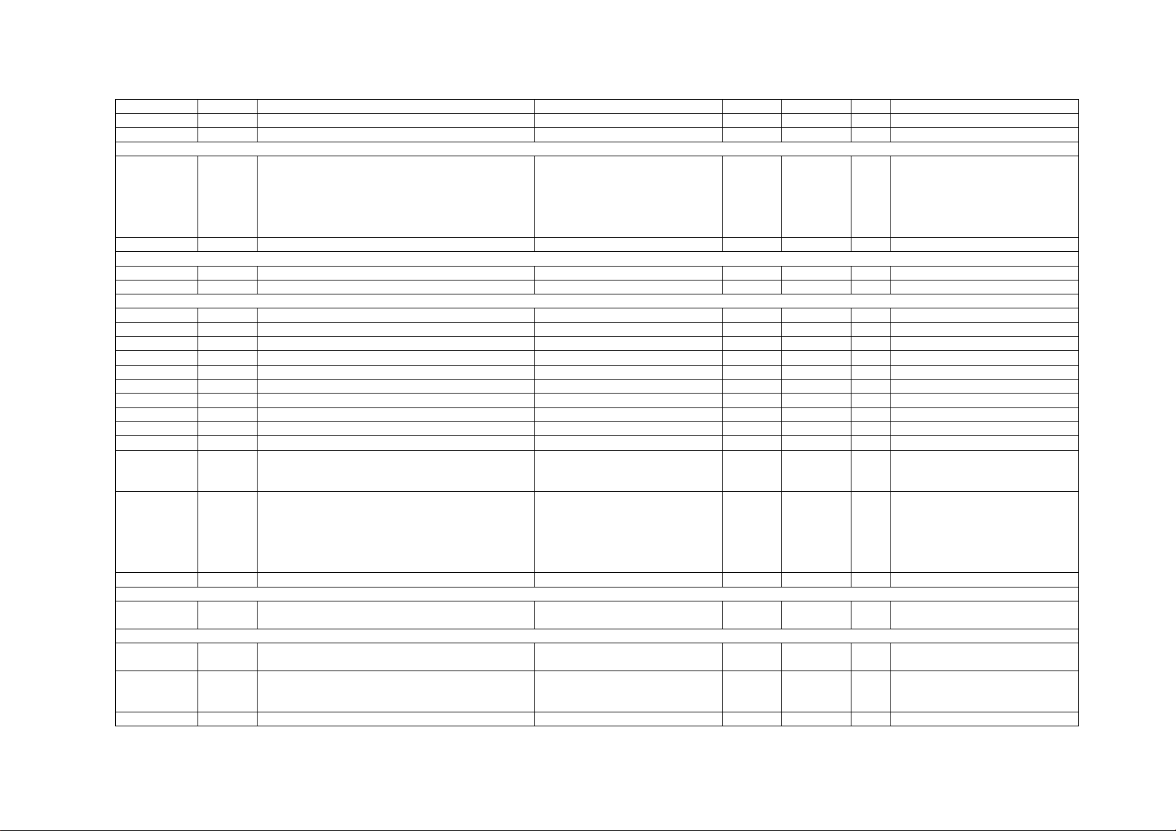
Address Point ID Description Options/Range Units Type R/W Notes
Write: 0=clear alarm, 1=no effect
44312-44325 Reserved
Device Diagnostics Register
44326-44327 Device diagnostics. Nonvolatile register.
44328-44341 Reserved
Current Port Number
44342 Active port number 0-2 = serial port COM1-COM3 UINT16 R
44343-44345 Reserved
Current Network Settings
44346-44367
+0,1 Ethernet network IP address UINT32 R Network byte order
+2,3 Ethernet network subnet mask UINT32 R Network b yte order
+4,5 Ethernet network default gateway UINT32 R Network byte order
+6,7 Not used UINT32 R
+8,9 Not used UINT32 R
+10,11 GPRS network IP Address UINT32 R Network byte order
+12,13 GPRS network subnet mask UINT32 R Network byte order
+14,15 GPRS network default gateway UINT32 R Network byte order
+16 Not used UINT32 R
+17 Cellular ne twork type 0 = 3GPP network (GSM, UMTS,
+18-21 Cellular mod ule’s mobile equipment identifier:
IMEI for 3GPP networks
MEID for 3GPP2 networks
44368-44377 Reserved
Device Authorization Registers
44378-44379 Write: 8-digit password. Read: 0 = access permitted,
-1 = authorization required.
Communication Status
44394 RSSI (received signal strength) 0 = not known or not detectable,
44395 GPRS status 0 = not connected,
44396-44409 Reserved UINT16 R 65535 = N/A
F23 UINT32 R/W Bitmap
LTE)
1 = 3GPP2 network (CDMA2000)
IMEI (15 decimal digits):
+18,19 – 8 lower digits in binary,
+20,21 – 7 higher digits in binary;
MEID (14 hex digits):
+18,19 – 8 lower digits,
+20,21 – 6 higher digits
0 - 99999999 (write)
0/-1 (read)
51-113 = -51 to -113 dBm
1 = not registered,
2 = registered
UINT32 R
UINT32 R
INT32 R/W
UINT16 R
UINT16 R
Read: 0=no faults logged, 1=
diagnostic failed at least once since
last reset;
Write: 0=clear diagnostic flag, 1=no
effect.
90

Address Point ID Description Options/Range Units Type R/W Notes
Communication Counters
44410 Successful eXpertPower client connections 0-65534 UINT16 R
44411 Failed eXpertPower client connections 0-65534 UINT16 R
44412 Successful TCP notification client connections 0-65534 UINT16 R
44413 Failed TCP notification client connections 0-65534 UINT16 R
44414-44441 Reserved UINT16 R 65535 = N/A
Factory Diagnostic Registers
45952-46079 Factory diagnostic registers UINT32 R
91

3.8 Device Setup Registers
Address Point ID Description Options/Range Units Type R/W Notes
Device Identification
46080-46111
+0,1 Device serial number 0-999999 UINT32 R
+2,3 Device model ID 72000 UINT32 R
+4-11 Device model name “EM720” CHAR16 R Null-terminated string
+12-13 Device options (bitmap) F27 UINT32 R
+14-15 Device production date and time F1 UINT32 R
+16-19 Not used UINT16 R
+20 Device firmware version number 2600-2699 UINT16 R Two higher decimal digits = major
+21 Device firmware build number 1-99 UINT16 R
+22 Transient coprocessor firmware version number 2700-2799 UINT16 R
+23 Transient coprocessor firmware build number 1-99 UINT16 R
+24 Boot loader vers i on number UINT16 R
+25 Boot loader build number 1-99 UINT16 R
+26-31 Not used UINT16 R
Factory Device Settings
46112-46178
+0 V1-V4 input range 480, 120 (option U) V UINT16 R
+1 V1-V4 input overload 125 % UINT16 R
+2,3 Not used UINT16 R
+4 I1-I4 input range 1, 5 A UINT16 R
+5 I1-I4 input overload 200 % UINT16 R
+6-13 Not used UINT16
+14-63 Reserved UINT16
+64 Ethernet MAC address 0-1 0x0500 UINT16 R
+65 Ethernet MAC address 2-3 0x00F0 UINT16 R
+66 Etherne t MA C address 4-5 0x0000-0xFFFF UINT16 R
Basic Setup
46208-46271
+0 Wiring mode F26 UINT16 R/W
+1 PT ratio (primary to secondary ratio) 10-65000
+2 PT secondary (line-to-line) voltage 50-480 V UINT16 R/W
+3-4 Reserved UINT16 R Read as 65535
+5 CT primary current 1-20000 A UINT16 R/W
+6 Reserved UINT16 R Read as 65535
+7 I4 CT primary current 1-20000 A UINT16 R/W
+8-16 Reserved UINT16 R Read as 65535
+17 Nominal line frequency 50, 60 Hz UINT16 R/W
×0.1
UINT16 R/W
version number, two lower decimal
digits = minor version number
92
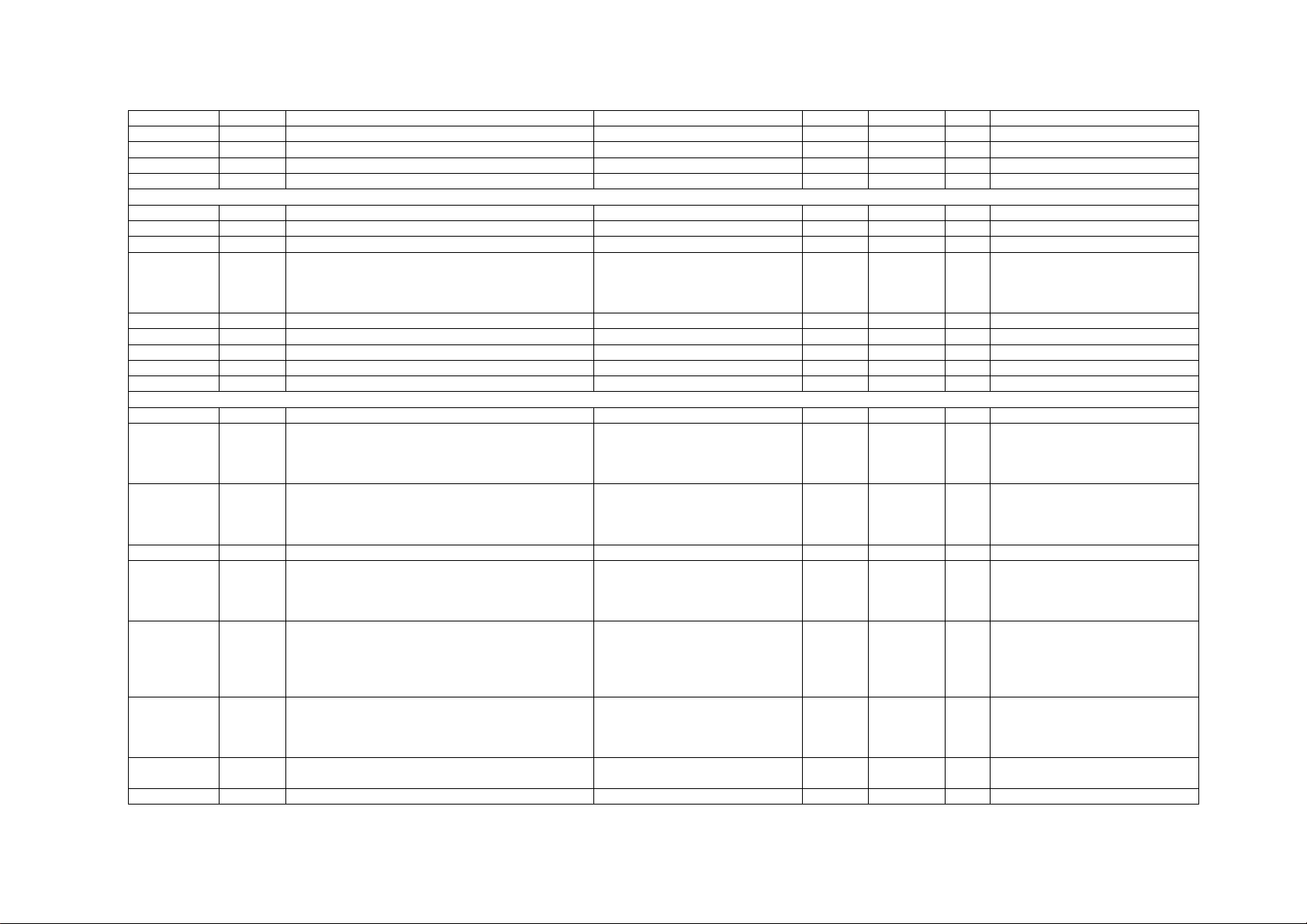
Address Point ID Description Options/Range Units Type R/W Notes
+18-23 Reserved UINT16 R Read as 65535
+24 I maximum demand load current 0-20000 A UINT16 R/W
+25 I4 maximum demand load current 0-20000 A UINT16 R/W
+26-31 Reserved UINT16 R Read as 65535
Demands Setup
46240-46255
+0 Power demand period (block interval) 1, 2, 3, 5, 10, 15, 30, 60 min UINT16 R/W
+1 Number of d emand p eriod s in a sl id ing wind ow 1-15 UINT16 R/W
+2 Demand sy nchronization source input 0 = device cloc k, 1-8 = DI1-DI8 UINT16 R/W A DI input is considered a pulse or
+3-7 Reserved UINT16 R/W Read as 65535
+8 Volt demand period 0-9000 sec UINT16 R/W
+9 Ampere demand period 0-9000 sec UINT16 R/W
+10 Harmonic demand period 0-9000 sec UINT16 R/W
+11-15 Reserved UINT16 R/W Read as 65535
Device Options Setup
46256-46271
+0 Power ca lculation mode 0 = using reactive power:
+1 Energy roll value 2 = 100,000.0 kWh
+2 Reserved UINT16 R/W Read as 65535
+3 End of billing (TOU/Billing maximum demand reset)
mode, bitmap
+4 Tariff control 0 = via a calendar scheduler,
+5 Number of tariffs 1-8 (does not have effec t with a
+6 PQ option 2 = EN 50160:2007
+7 Energy LED test mode 0 = disabled, 1 = enabled UINT16 R/W
S = f(P,Q),
1 = using non-active power:
Q=f(S,P)
3 = 1,000,000.0 kWh
4 = 10,000,000.0 kWh
5 = 100,000,000.0 kWh (default)
Bit 0 = 1 – automatic/monthly
mode allowed
Bit 1 = 1 - COM mode allowed
Bit 2 = 1 - manual mode allowed
0x4000 = via communications,
0x0100-0x0107 = via tariff inputs
DI1-DI8 (bits 0:2 denote the first
digital input index used)
calendar tariff control option)
5 = EN 50160:2010
UINT16 R/W
UINT16 R/W
UINT16 R/W
UINT16 R/W
UINT16 R/W When read with a calendar tariff
UINT16 R/W V26.XX.20 and later
KYZ input. The pulse edge restarts
the power demand accumulation
interval.
control option, indicates the actual
number of tariffs selected in TOU
profiles
93
Address Point ID Description Options/Range Units Type R/W Notes
+8 Energy LED pulse rate, Wh/impulse, varh/impulse (in
secondary units)
+9-15 Reserved UINT16 R/W Read as 65535
Local Settings
46400-46415
+0 Local time offset, min 0-+/-720 min INT16 R/W
+1 Dayl ig ht savings time (DST) option 0=DST disabled (stand ard time
+2 DST start month 1-12 UINT16 R/W
+3 DST start week of the month 1=1st, 2=2nd, 3=3rd, 4=4th week,
+4 DST start weekday 1-7 (1=Sun, 7=Sat) UINT16 R/W
+5 DST end month 1-12 UINT16 R/W
+6 DST end week of the month 1=1st, 2=2nd, 3=3rd, 4=4th week,
+7 DST end weekda y 1-7 (1=Sun, 7=Sat) UINT16 R/W
+8 Cloc k synchronization source 0=IRIG-B,
+9 Coun try code ITU country calling code UINT16 R/W
+10 DST start hour 1-6 UINT16 R/W
+11 DST end hour 1-6 UINT16 R/W
+12-15 Reserved UINT16 R/W
Clock Indication and Setup
46416-46447
+0,1 Local time, in seconds, since Jan 1, 1970 F1 sec UINT32 R/W
+2,3 Fractional seconds, µsec µsec UINT32 R/W
+4 Fractional seconds, milliseconds 0-999 ms UINT16 R/W
+5 Seconds 0-59 UINT16 R/W
+6 Minutes 0-59 UINT16 R/W
+7 Hour 0-23 UINT16 R/W
+8 Day of month 1-31 UINT16 R/W
+9 Month 1-12 UINT16 R/W
+10 Year (calendar year minus 2000) 0-99 UINT16 R/W
+11 Weekday 1-7 (1=Sun, 7=Sat) UINT16 R
+12 Daylight savings time sta tus 0=standard time is active,
+13-31 Reserved UINT16
1-40
only),
1=DST enabled (fixed switching
dates),
2= scheduled DST period (calendar
defined switching dates)
5=the last week of the month
5=the last week of the month
1-8 = DI1-DI8,
0xfffe = SNTP,
0xffff = none
1=daylight saving time is active
×0.01Wh
UINT16 R/W
UINT16 R/W
UINT16 R/W
UINT16 R/W A DI input is considered a pulse or
UINT16 R
UINT16 R/W
KYZ input. The pulse edge adjusts
the clock at the nearest whole
minute.
94
Address Point ID Description Options/Range Units Type R/W Notes
Communication Ports Setup
46448-46495
+0 Communication protocol 0 = Modbus RTU, 1 = Modbus
ASCII, 2 = DNP3.0,
6 = IEC 62056-21,
7 = IEC 61850
+1 Interface 0 = RS-232, 1 = RS-422, 2 = RS-
485, 3 = Infrared, 8 = GSM/GPRS
+2 Device address Modbus: 1-247
DNP3.0: 0–65532
+3 Baud rate 3 = 1200 bps, 4 = 2400 bps, 5 =
4800 bps, 6 = 9600 bps, 7 = 19200
bps, 8 = 38400 bps, 9 = 57600 bps,
10 = 115200 bps
+4 Data format 0 = 7 bits/even parity,
1 = 8 bits/no parity,
2 = 8 bits/even parity
+5 CTS mode 0 = not used, 1 = wait for CTS
before sending data
+6 RTS mode 0 = not used,
1 = RTS is asserted during the
transmission
+7 Minimum delay before sending data 0-1000 (default = 5) ms UINT16 R/W
+8 Inter-character time-out 0-1000 (default = four-character
time)
+9 Port direction 0 = slave (default), 1 = master UINT16 R/W
+10 Receive timeout (for a master port only) 500-30000 ms UINT16 R/W
+11-15 Reserved Read as 65535
46448-46463 COM1 Setup
46464-46479 COM2 Setup
46480-46495 COM3 Setup
Network Setup
46576-46703
+0,1 Device IP Address 0x01000000-0xFFFFFFFF UINT32 R/W Network byte order
+2,3 Network subnet mask 0x00000001-0xFFFFFFFF UINT32 R/W Network byte order
+4,5 Network default gateway 0x00000000-0xFFFFFFFF UINT32 R/W Network byte order
+6-31 Reserved R/W
Dial-up/GPRS Modem Setup
46640-46671
+0,1 Device IP Address 0x01000000-0xFFFFFFFF UINT32 R/W
+2,3 Network subnet mask 0x00000001-0xFFFFFFFF UINT32 R/W
+4,5 Network default gateway 0x00000000-0xFFFFFFFF UINT32 R/W
+6,7 Number of dial attempts 0–1000, 0-dial forever UINT32 R/W
+8,9 Connection timeout, sec 0-9999 UINT32 R/W
UINT16 R/W
UINT16 R/W
UINT16 R/W
UINT16 R/W
UINT16 R/W
UINT16 R/W N/A for COM1-COM3 (read as
65535)
UINT16 R/W N/A for COM1-COM3 (read as
65535)
ms UINT16 R/W
95

Address Point ID Description Options/Range Units Type R/W Notes
+10,11 Delay between redials, sec 0-9999 UINT32 R/W
+12,13 Idle connection timeout, sec 0-9999, 0 = never UINT32 R/W
+14,15 Number of rings before answer 0-20, 0 = never answer UINT32 R/W
+16-23 Modem init string “AT&F&D1&C1” CHAR16 R/W Null-terminated string
+24-31 Reserved
Password Setup
46704-46711
+0,1 Password 1 (Low level) 0-99999999 UINT32 R/W Read as 0
+2,3 Passw ord protection (always ON) 1 = enabled UINT16 R/W
+4,5 Password 2 (Medium level) 0-99999999 UINT32 R/W Read as 0
+6,7 Password 3 (High level) 0-99999999 UINT32 R/W Read as 0
IEC 61850 License Setup
46762-46767
+0,1 License code, first word UINT32 R/W
+2,3 License code, second word UINT32 R/W
+4,5 Current license type 0=no valid license
1-31=temporary license, remaining
time in days
-1=permanent license
-3=temporary license has expired
Expert Power Service Setup
46768-46783
+0,1 Expert Power server IP Address 0x01000000-0xFFFFFFFF UINT32 R/W Default = 207.232.60.18
+2,3 Expert Power server TCP service port 0-65535 UINT32 R/W Default = 5001
+4,5 E x pert Power client enabled 0 = client disabled, 1 = client
enabled
+6,7 Time to next session 1-99999 min UINT32 R/W
+8,9 Time to next session 1-99999 min UINT32 R Same as previous
+10,11 Connection network 0 = Ethernet, 1=GPRS UINT32 R/W
+12-15 Reserved
Internet Service Provider (ISP) account
46784-46879
+0-15 Dial string (telephone number) “*99#” CHAR32 R/W GPRS network by default
+16-31 Login name CHAR32 R/W
+32-47 Login password CHAR32 R/W
+48-63 Access Point Name (APN) CHAR32 R/W
+64-95 Reserved
SNTP Client Setup
46880-46895
+0,1 SNTP client enabled 0 = disabled, 1 = enabled UINT32 R/W
+2,3 Polling interval 60-86400 s UINT32 R/W Default = 600 s
+4-7 Reserved 0 UINT32 R/W
+8,9 Primary SNTP server IP address 0x01000000-0xFFFFFFFF UINT32 R/W Default = 192.36.143.151
UINT32 R
UINT32 R/W
96

Address Point ID Description Options/Range Units Type R/W Notes
+10,11 Secondary SNTP server IP address 0x01000000-0xFFFFFFFF UINT32 R/W Default = 130.149.17.21
+12-15 Reserved
TCP Notification Client Setup
46896-46991
+0,1 Client enabled 0 = disabled, 1 = enabled UINT32 R/W
+2,3 Server address 0x01000000-0xFFFFFFFF UINT32 R/W
+4,5 Server port 0-65535 UINT32 R/W
+6,7 Message exchange address 0-65535 UINT32 R/W
+8,9 Conne ct ion network 0 = Ethernet, 1=GPRS UINT32 R/W
+10-15 Reserved
Transformer Correction Setup
47072-47223
+0 Channel 0=not used, 1-3=V1-V3, 5-8=I1-I4 UINT16 R/W
+1 Test point, percent of nominal 5-200 % UINT16 R/W
+2 Ratio correction factor 900-1100
+3 Phase angle error -600 to 600 min INT16 R/W
47072-47075 Transformer correction point 1
47076-47079 Transformer correction point 2
… …
47220-47223 Transformer correction point 56
Transformer/Line Loss Compensation Setup
47328-47375
+0,1 Metering point location 0=supply side, far end;
1=supply side, transformer end;
2=load side, transformer end;
3=load side, far end.
+2,3 Billing point location 0=supply side, far end;
1=supply side, transformer end;
2=load side, transformer end;
3=load side, far end.
+4,5 Number of the metering elements 2-3 UINT32 R/W
+6,7 Rated transformer primary voltage 0-1500000 UINT32 R/W
+8,9 Rated transformer secondary voltage 0-1500000 UINT32 R/W
+10,11 Rated transformer kVA 0-1000000 kVA UINT32 R/W
+12,13 No-load iron watt loss 0-1000000 watt UINT32 R/W
+14,15 Full-load copper watt loss 0-1000000 watt UINT32 R/W
+16,17 Percent excitation current 0-100000 0.001% UINT32 R/W
+18,19 Full-load percent impedance 0-100000 0.001% UINT32 R/W
+20,21 Supply-side power line length 0-10000000 0.0001
+22,23 Supply-side power line resistance 0-100000 0.001
+24,25 Supply-side power line reactance 0-100000 0.001 UINT32 R/W
×0.001
UINT32 R/W
UINT32 R/W
km/miles
Ohm/km,
Ohm/mile
UINT16 R/W
UINT32 R/W
UINT32 R/W
97

Address Point ID Description Options/Range Units Type R/W Notes
Ohm/km,
Ohm/mile
+26,27 Load-side power line length 0-10000000 0.001
+28,29 Load-side power line resistance 0-100000 0.001
+30,31 Load-side power line reactance 0-100000 0.001
+32,33 Iron watt percent loss constant (%LWFe) 0-1000000 0.0001% UINT32 R/W
+34,35 Copper watt percent loss constant (%LWCu) 0-1000000 0.0001% UINT32 R/W
+36,37 Iron var percent loss constant (%LVFe) 0-1000000 0.0001% UINT32 R/W
+38,39 Copper var percent loss constant (%LVCu) 0-1000000 0.0001% UINT32 R/W
+40-47 Reserved 0 UINT32 R/W
Display Setup
48664-48695
+0 Reserved UINT16 R
+1 A u to-scroll interval 0 = disabled,
1-10, 15, 20, 25, 30
+2 Auto-return interval 0 = disabled,
1-5, 10, 15, 20, 25, 30
+3 Backlight time 0 = disabled, 1-10 min UINT16 R/W
+4 Reserved UINT16 R/W
+5 Auto-scroll sequence, bitmap 0-0x01FF
Bits 0-8: bit=1– display is included
in a scroll sequence
+6 Diagnostics message icon 0 = disabled
1 = enabled
+7 Default page Bits 0-7 = page number (0-9)
Bits 8-15 = display number (0-8)
+8-31 Reserved UINT16 R/W
GOOSE Publisher Setup
49046-49145
+0 Publisher number 0 UINT16 R/W Write number first before reading
+1 A ct ivate Write: 1=activate UIN T 1 6 R/W Write 1 to store and activate setup
+2-34 Goose control block reference “MET1/LLN0$GO$GoCBPub1" CHAR66 R
+35 Publisher enabled 0 = disabled, 1 = enabled UINT16 R/W
+36-51 GOOSE application identifier "Pub1" CHAR34 R
+53-85 Data set reference “MET1/LLN0$DSetGOOSE1" CHAR66 R
+86-87 Configuration revision 1 UINT32 R/W Default = 1
+88 Needs commissioning 0 = no, 1= yes UINT16 R Default = 0
+89-91 Destination MAC address (multicast) 01:0C:CD:01:00:00 to CHAR6 R/W Default = 01:0C:CD:01:01:FF
km/miles
Ohm/km,
Ohm/mile
Ohm/km,
Ohm/mile
sec UINT16 R/W
min UINT16 R/W
UINT16 R/W
UINT16 R/W
UINT16 R/W
UINT32 R/W
UINT32 R/W
UINT32 R/W
following registers
98

Address Point ID Description Options/Range Units Type R/W Notes
01:0C:CD:01:01:FF
+92 Destination VLAN priority 4 UINT16 R Default = 4
+93 Destination VLAN ID 0 UINT16 R Default = 0
+94 Destination application ID 0-0xFFFF UINT16 R/W Default = 3001
+95 Maximum retransmission interval 500-60000 ms UINT16 R/W Default = 5000
+96-99 Not used
IEC 61850 IED Setup
49146-49209
+0-11 IED name CHAR24 R/W
+12-19 Subnet name CHAR16 R/W
+20 Connection idle timeout 1-10 min UINT16 R/W
+21 Voltage units 0=V, 1=kV UINT16 R/W
+22 Current units 0=A, 1=kA UINT16 R/W
+23 Power units 0=kW, 1=MW UINT16 R/W
+24 Maximum instances/clients per RCB 0=non-indexed, 1, 2, 4 UINT16 R/W
+25-30 Location CHAR32 R/W
+31-63 Not used 0 UINT16 R/W
IEC 61850 Dataset Setup
49210-49278
+0 R e ad : current dataset number
Write: number of dataset members
+1 A ct ivate Write: 1=activate UIN T 1 6 R/W Write 1 to store and activate setup
+2-34 Dataset reference CHAR66 R/W
+35 Dataset member number 0-63 UINT16 R/W Write a dataset member number
+36-68 Dataset member reference CHAR66 R/W
IEC 61850 RCB Setup
49280-49351
Command registers Write 1-2 registers for a command
+0 Read command (moves the list pointer to the first
item in a list)
+1 A ct ivate 1=activate UINT16 W Write to store and activate setup
RCB registers (read/write) UINT16 R/W Write more than 2 registers to
+0 RCB type: 1=BRCB, 2=URCB UINT16 R/W
+1 Not used UINT16 R/W
+2-18 RptID CHAR34 R/W
+19 RptEna UINT16 R/W
+20-52 Dataset reference CHAR66 R/W
+53 Not used UINT16 R/W
+54,55 ConfRev UINT32 R/W
+56,57 OptFlds UINT32 R/W
+58,59 BufTm UINT32 R/W
1-16/1-64 UINT16 R/W Write a dataset number before
0xF0F0=read RCBs list,
0xE0E0=read dataset references list
UINT16 W Write a command before reading
reading dataset registers
before reading following registers
setup registers
change setup
99

Address Point ID Description Options/Range Units Type R/W Notes
+60 SqNum UINT16 R/W
+61 TrgOps UINT16 R/W
+62,63 IntgPd UINT32 R/W
+64 Resv UINT16 R/W
+65-71 RCB name (logical_device/rcb_name) CTRL/rcb_name
Dataset references list (read)
+19 Dataset number UINT16 R
IEC 61850 Report Deadbands
49396-49426 See F28 for measured value indices
+0 Measured value 1 deadband 1-50000
… … 1-50000
+30 Measured value 49 deadband 1-50000
49427-49459 Reserved Read as 65535
DNP Options Setup
51158-51183
+0 Default Binary Input Static object variation F24 (default 0) UINT16 R/W
+1 Default Binary Input Change object variation F24 (default 1) UINT16 R/W
+2 Default Binary Counter object variation F24 (default 3) UINT16 R/W
+3 Default Frozen Binary Counter object variation F24 (default 4) UINT16 R/W
+4 Reserved UINT16 R/W
+5 Default Binary Counter Change Event object variation F24 (default 2) UINT16 R/W
+6 Default Analog Input object variation F24 (default 3) UINT16 R/W
+7 Reserved UINT16 R/W
+8 Reserved UINT16 R/W
+9 Default Analog Input Change Event object variation F24 (default 2) UINT16 R/W
+10 Re-mapping static point indices for event objects 0=disabled (default), 1=enabled UINT16 R/W
+11 16-bit BC Scaling
+12 16-bit AI Scaling 0=disabled, 1=enabled (default) UINT16 R/W
+13 Number of points allocated for Analog Input change
events
+14 Number of points allocated for Binary Input change
events
+15 Number of points allocated for Binary Counter change
events
+16 Select/Operate Timeout 2 to 30 seconds (default 10 sec) UINT16 R/W
+17 Multi Fragment Interval 50 to 500 ms (default 50 ms) UINT16 R/W
+18-21 Reserved Read as 65535 UINT16 R/W
+22,23 Time Sync Period 1 to 86400 seconds (default 86400
+24 Voltage scale, volts secondary 60 to 480V (default 144V) V UINT16 R/W
+25 Current scale, amps secondary 100-500
MET1/rcb_name
0=×1 (default), 1=×10, 2=×100,
3=×1000
0 to 64 (default 32) UINT16 R/W
0 to 32 (default 0) UINT16 R/W
0 to 64 (default 0)
sec)
CHAR14 R/W Reading register 71 advances to the
×0.001%
×0.001%
×0.001%
UINT16 R/W
UINT16 R/W
UINT32 R/W
×0.1A
UINT16 R/W
UINT16 R/W
UINT16 R/W
UINT16 R/W
next RCB in the list
100
 Loading...