SaRonix
Crystal Clock Oscillator
S1800 / S1803 / S1850 Series
Technical Data
3.3 & 5V, HCMOS, TTL, SMD
DS-181 REV F01
(T) = Tape & Reel
full reel increments only
Frequency Range:
Frequency Stability: ±25, ±50, ±100 ppm over all conditions; calibration, tolerance,
operating temperature, input voltage change, load change, aging
(1 Year @ 25°C average ambient temperature), shock and vibration.
1.5440 MHz to 80 MHz
Temperature Range:
Operating:
Storage:
Supply Voltage:
-10 to +70°C or -40 to +85°C
-55 to +125°C
+5.0V ±10%, 3.3V ±10%
Supply Current:
Description
The 5V S1800, S1850 and 3.3V S1803
are crystal-controlled, low-current oscillators providing precise rise and fall
times to drive high speed CMOS and
TTL loads. The sub-miniature, very
low profile leadless ceramic packages
have gold-plated contact pads, ideal
for today's pick-and-place SMT environments. The S1850 is a high output
load version available to 80 MHz.
ACTUAL SIZE
S1800
25mA max
35mA max
10µA max
S1803
15mA max
18mA max
25mA max
10µA max
S1850
27mA max
35mA max
75mA max
1.544 to 32 MHz:
32+ to 50 MHz:
50+ to 80 MHz:
1.544 to 50 MHz (standby):
1.544 to 80 MHz (standby):
Standby Current: 10µA max on S1800 and S1803 only
Output:
Symmetry:
Rise & Fall Times:
Logic 0:
Logic 1:
Load:
45/55% max @ 50% VDD, 40/60% max @ 1.5V on S1800 & 1850
7ns max (10ns max: S1800) 20% to 80% V
DD,
1.544 to 50 MHz
5ns max, 50+ to 80 MHz (S1803 & S1850 only)
10% VDD max
90% VDD min
Applications & Features
•
•
•
•
•
•
Sub-miniature, 1.1 mm high ceramic
package ideal for SMT applications
10µA max standby mode on S1800
and S1803
Available as 3.3V and 5V versions
CMOS, HCMOS & TTL compatible
Perfect for PC's; notebook, palmtop
computers; portable applications;
PCMCIA cards;disc drives. Anywhere
small size, low power, surface
mountability are a priority
Available on tape & reel; 16mm tape,
1000pcs per reel
Solder Reflow Guide
Reflow 240 max
Preheat 183 ±10°C
4°C/sec max
Temperature – °C
4°C/sec max
1 – 2 minutes 10 sec maxTime
150
200
250
Cooling
S1800/S1803:
S1850:
15 pF max, 10 LSTTL
50 pF max 1.544 to 50 MHz, 10 TTL
30 pF max 50+ to 70 MHz, 10 TTL
20 pF max 70+ to 80 MHz (HCMOS), 10 TTL
Part Numbering Guide
Mechanical:
Shock:
Solderability:
Vibration:
Solvent Resistance:
Terminal Strength:
Resistance to Soldering Heat:
MIL-STD-883, Method 2002, Condition B
MIL-STD-883, Method 2003
MIL-STD-883, Method 2007, Condition A
MIL-STD-202, Method 215
MIL-STD-883, Method 2004, Condition D
MIL-STD-202, Method 210, Condition I or J
Environmental:
Gross Leak Test:
Fine Leak Test:
Thermal Shock:
Moisture Resistance:
MIL-STD-883, Method 1014, Condition C
MIL-STD-883, Method 1014, Condition A2
MIL-STD-883, Method 1011, Condition A
MIL-STD-883, Method 1004
Series
S1800 = 5.0V, 1.544 to 50 MHz, 15 pF, standby
S1803 = 3.3V, 1.544 to 80 MHz, 15 pF, standby
S1850 = 5.0V, 1.544 to 80 MHz, 50 pF high drive
S 1803 C – 60.0000 (T)
Saronix
Frequency (MHz)
Stability Tolerance
A = ±25 ppm, -10 to +70°C
B = ±50 ppm, -10 to +70°C
C = ±100 ppm, -10 to +70°C
E = ±50 ppm, -40 to +85°C
F = ±100 ppm, -40 to +85°C
SaRonix
141 Jefferson Drive • Menlo Park, CA 94025 • USA • 650-470-7700 • 800-227-8974 • Fax 650-462-9894
8ps max RMS period jitterJitter:
查询S1850C-60.0000供应商

SaRonix
Crystal Clock Oscillator
3.3 & 5V, HCMOS, TTL, SMD
S1800 / S1803 / S1850 Series
Technical Data
All specifications are subject to change without notice.
DS-181 REV F01
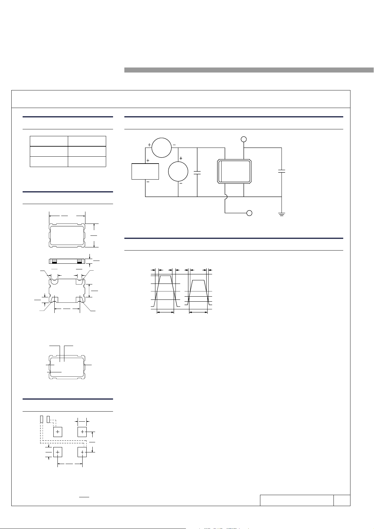
Tri-State Logic Table Test Circuit
Scale: None (Dimensions in )
mm
inches
Pad 1 Input
Logic 1 or NC
Logic 0 or GND
Pad 3 Output
Oscillation
High Impedance
Required Input Levels on Pad 1:
Logic 1 = 2.2V min
Logic 0 = 0.8V max
Package Details
7.5
.295
max
5.2
.205
max
1.15
.043
1.4
.055
Pad 2
(GND)
Pad 1
(Tri-State
Control)
2.6
.102
5.08
.200
Pad 3
(OUT)
Pad 4
(VDD)
1.1
.043
max
Output Waveform
SaRonix
Frequency
Date Code
S 5 C
5 = S1800
9 = S1803
B = S1850
Stability Tolerance
Marking Format
*
C
L
= S1800/S1803: 15 pF
S1850: 50 pF to 50 MHz
30 pF, 50+ to 70 MHz
20 pF, 70+ to 80 MHz
(Note A)
POWER
SUPPLY
mA
M
V M
TEST
POINT
OUTV
DD
OSCILLATOR
GND
Pad 2
Pad 1
Pad 4
Pad 3
0.1 µF
TRI-STATE INPUT
Note A: CL includes probe and fixture capacitance
Recommended Land Pattern
*
Exact location of items may vary
1.8
.071
2.0
.079
4.2
.165
5.08
.200
YY WW
**
External high frequency power supply
decoupling required.
**
2.5 VDC
1.5 VDC
0.5 VDC
T
f
T
f
T
r
T
r
HCMOS TTL
SYMMETRY SYMMETRY
GND
VDD
LOGIC 0
20% VDD
50% VDD
80% VDD
LOGIC 1
12
43
SaRonix
141 Jefferson Drive • Menlo Park, CA 94025 • USA • 650-470-7700 • 800-227-8974 • Fax 650-462-9894
1.0
.039
 Loading...