查询NCH030xxx供应商
SaRonix
Technical Data
ACTUAL SIZE
Description
A crystal controlled, low current, low
jitter and high frequency oscillator with
precise rise and fall times demanded in
networking applications. The tri-state
function on the NTH enables the output
to go high impedance. Device is packaged in a 14 or an 8-pin DIP compatible
resistance welded, all metal grounded
case to reduce EMI. True SMD DIL14
versions for IR reflow are available, select option "S" in part number builder.
See separate data sheet for SMD package
dimensions.
Applications & Features
ADSL, DSL
•
DS3, ES3, E1, STS-1, T1
•
Ethernet Switch, Gigabit Ethernet
•
Fibre Channel Controller
•
MPEG
•
Network Processors
•
Voice Over Packet
•
32 Bit Microprocessors
•
Tri-State output on NTH
•
LVCMOS / HCMOS compatible
•
Available up to 106.25 MHz
•
Crystal Clock Oscillator
Frequency Range:
Frequency Stability:
Temperature Range:
Operating:
Storage:
Supply Voltage:
Recommended Operating: 3.3V ±10%
Supply Current: 20mA max, 0.5 to 30 MHz
Output Drive:
HCMOS
Rise and Fall Times:
Mechanical:
Resistance to Soldering Heat:
Environmental:
Moisture Resistance:
Symmetry:
Logic 0:
Logic 1:
Load:
Period Jitter RMS:
Shock:
Solderability:
Terminal Strength:
Vibration:
Solvent Resistance:
Gross Leak Test:
Fine Leak Test:
Thermal Shock:
0.5 MHz to 106.25 MHz
±20, ±25, ±50 or ±100 ppm over all conditions: calibration
tolerance, operating temperature, input voltage change,
load change, 30 day aging, shock and vibration.
0 to +70°C or -40 to +85°C, See Part Numbering Guide
-55 to +125°C
25mA max, 30+ to 50 MHz
30mA max, 50+ to 80 MHz
35mA max, 80+ to 106.25 MHz
45/55% max 0.5 to 70 MHz max
40/60% max @ 50% V
4ns max 0.5 to 50 MHz, 20% to 80% V
3ns max 50+ to 80 MHz
1.5ns max 80+ to 106.25 MHz
10% VDD max
90% VDD min
50 pF, 0.5 to 50 MHz
30pF, 50+ to 70 MHz
15pF, 70+ to 106.25 MHz
8ps max
MIL-STD-883, Method 2002, Condition B
MIL-STD-883, Method 2003
MIL-STD-883, Method 2004, Conditions A & C
MIL-STD-883, Method 2007, Condition A
MIL-STD-202, Method 215
MIL-STD-202, Method 210, Condition A, B or C
MIL-STD-883, Method 1014, Condition C
MIL-STD-883, Method 1014, Condition A2
MIL-STD-883, Method 1011, Condition A
MIL-STD-883, Method 1004
3.3V, LVCMOS / HCMOS, Tri-State
DD
NTH / NCH Series
DD
Output Waveform
Logic 1
80% V
DD
50% V
DD
20% V
DD
Logic 0
SaRonix
T
r
SYMMETRY
CMOS
T
f
DS-159 REV D
141 Jefferson Drive • Menlo Park, CA 94025 • USA • 650-470-7700 • 800-227-8974 • Fax 650-462-9894

SaRonix
Crystal Clock Oscillator
Technical Data
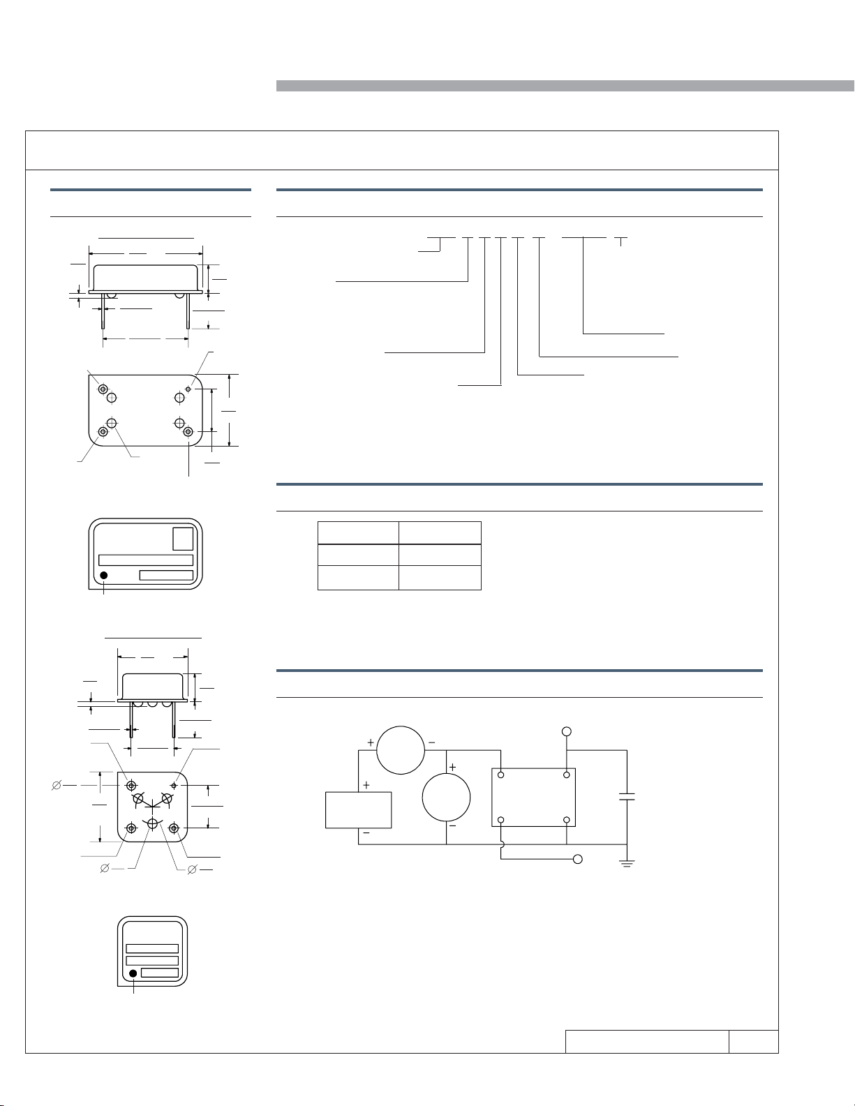
Package Details Part Numbering Guide
FULL SIZE PACKAGE
21.0
0.91
.036
max
Pin 1
Tri-State - NTH
N/C - NCH
Pin 14
+3.3 VDC
Standard Marking Format
Includes Date Code, Frequency & Part Number
.825
.46±.08
.018±.003
15.24±.13
.600±.005
(4) Glass
Insulators
max
6.35±0.51
0.25±0.02
Pin 8 Output
**
7.75
.305
5.08
.200
Pin 7
GND
13.0
.510
max
max
NTH = Pin 1: Tri state, LVCMOS
NCH = Pin 1: N/C, LVCMOS
Symmetry
0 = 40/60% max, 0 to 70°C
2 = 40/60% max, -40 to 85°C
A = 45/55% max, 0 to 70°C, 70 MHz max
C = 45/55% max, -40 to 85°C, 70 MHz max
Frequency Range
3 = 0.5 to 6 MHz
6 = 6+ to 24 MHz
8 = 24+ to 106.25 MHz
max
Tri-State Logic Table (NTH only)
3.3V, LVCMOS / HCMOS,
NTH / NCH Series
NTH 0 8 0 C 3 - 40.0000 (T)
Packing Method
(T) = Tape & Reel for SMD versions,
full reel increments only, 200pcs (full
size) or 250pcs (half size)
Blank = Bulk
Frequency (MHz)
3.3V Supply
Package
0 = Full Size, Thru-Hole
9 = Half Size, Thru-Hole
K = Full Size, Gull Wing
J = Half Size, Gull Wing
N = Half Size, Gull Wing, Spanked Leads
S = Full Size, True SMD Adaptor (see separate data sheet for dimensions)
Stability Tolerance
C = ±100ppm
B = ±50ppm
A = ±25ppm, 0 to +70°C only
AA = ±20ppm, 0 to +70°C only
SARONIX
XTAL OSC
Denotes Pin 1
HALF SIZE PACKAGE
13.0
max
.510
0.91
max
.036
.46±.08
.018±.003
Pin 1
Tri-State - NTH
N/C - NCH
1.5
.059
13.0
.510
max
Pin 8
+3.3 VDC
Standard Marking Format
Includes Date Code, Frequency & Part Number
1.7
.067
7.62±.20
.300±.008
120°
120°
120°
5.08
.200
6.35±0.51
0.25±0.02
7.62±.20
.300±.008
6.0
.236
**
SARONIX
max
Pin 4
GND
Pin 5
Output
Logic 1 or NC
Logic 0 or GND
Internal Pullup Resistance
Test Circuit
Pin 1 Input
POWER
SUPPLY
Pin 8 (5) Output
Oscillation
High Impedance
Output:
Output:
Required Input Levels on Pin 1:
Logic 1 = 2.2V min
Logic 0 = 0.8V max
Oscillation @ VIN, 2.2V min
High Impedance @ VIN, 0.8V max
50KΩ min
Control Input:
mA
M
NOTE A: CL includes probe and fixture capacitance
*( ) Indicates pin numbers for half-size package
Disable Output Delay: 100ns max
TEST
POINT
Pin 14 (8)
VDD
OUT
V M
Pin 1 (1)*
OSCILLATOR
GND
TRI-STATE INPUT (NTH only)
Pin 8 (5)
Pin 7 (4)
CL = 50 pF, 0.5 to 50 MHz
CL = 30 pF, 50+ to 70 MHz
CL = 15pF, 70+ to 106.25 MHz
(Note A)
**
Exact location of items may vary
SaRonix
Denotes Pin 1
All specifications are subject to change without notice.
DS-159 REV D
141 Jefferson Drive • Menlo Park, CA 94025 • USA • 650-470-7700 • 800-227-8974 • Fax 650-462-9894

Technical Data
SaRonix
True SMD Adaptor - 7.57mm High
SaRonix
REV A
141 Jefferson Drive • Menlo Park, CA 94025 • USA • 650-470-7700 • 800-227-8974 • Fax 650-462-9894
 Loading...