

Page 1
1
Sapphire Instruments Co., Ltd.
Calibration Procedure of SI-9002
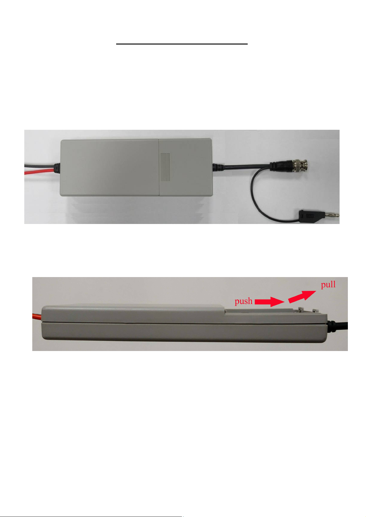
1. How to open the case, please follow the steps.
1.1 Remove the battery lid.
1.2 You will see the two screws and loosen them.
Fig. 1
1.3 Near the BNC cable side, there are two protuberant mortises. Use fingers to push back and pull
upward.
Fig. 2
Page 2
2
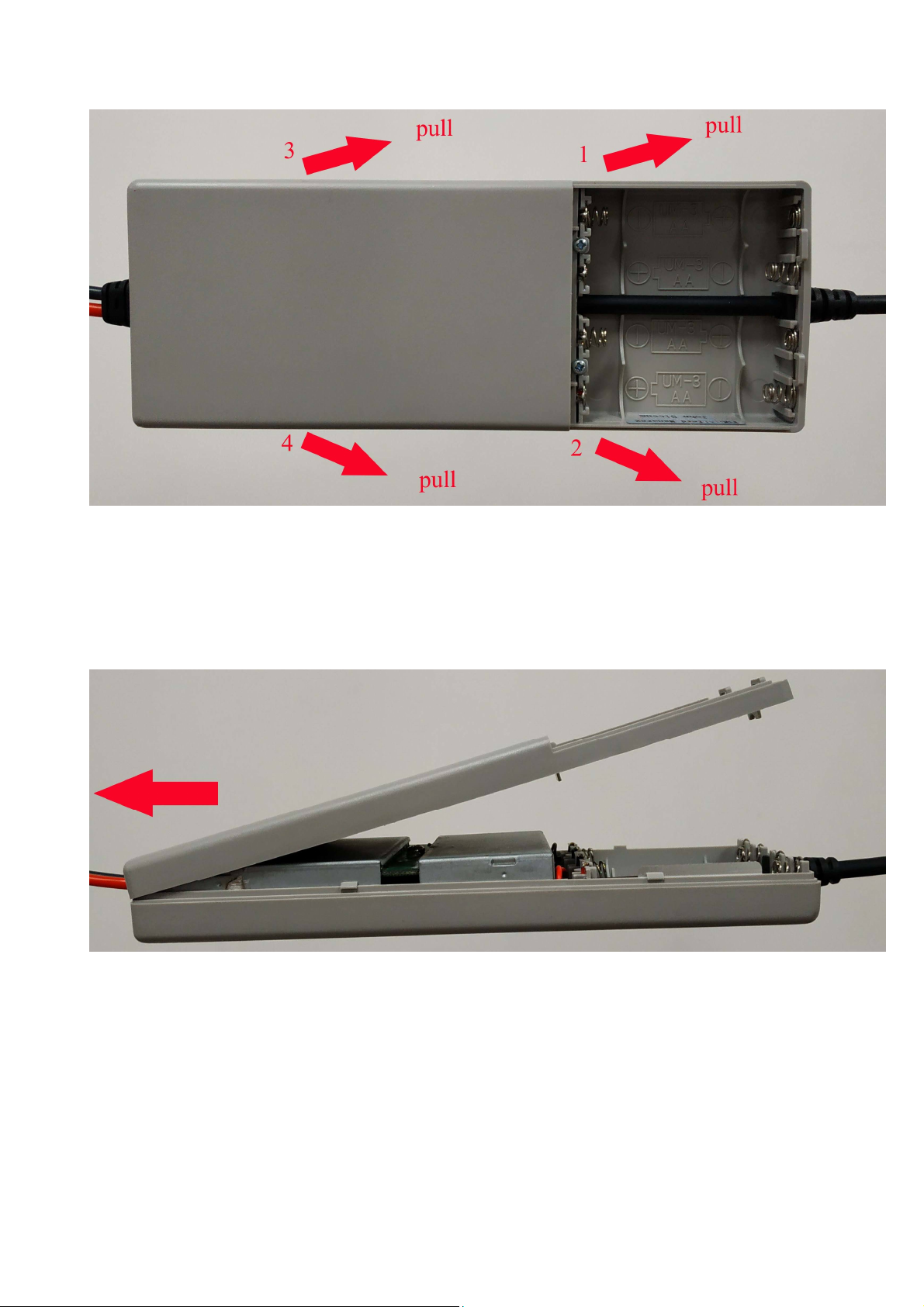
1.4 Use fingers to press the bottom case inward, and pull it backward and upward.
Fig.3
1.5 Hold the bottom case and push back (to input lines
direction).
Fig.4
Page 3
3
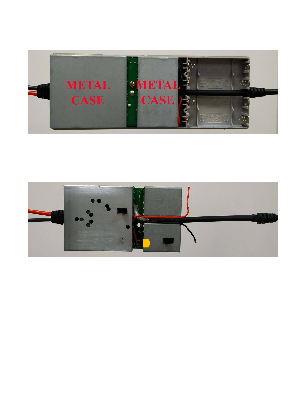
1.6 You will see the two metal cases. There is one screw on the PCB. Loosen it, then the whole metal case
can be taken out. There are two wires still connected with the upper case. Leaves them
there.
Fig. 5
1.7 The metal case is illustrated as follows:
Fig. 6
2. Explanation of adjustment point. Please refer to Fig. 7.
(1) SW1: Switch for selecting attenuation ratio.
(2) SW2: Power switch.
(3) VR4: Variable resistor for adjusting offset when SW1 at attenuation 1/200.
(4) VR2: Variable resistor for adjusting offset when SW1 at attenuation 1/20.
(5) VR1: Variable resistor for adjusting low frequency CMRR.
(6) VR3: Variable resistor for adjusting accuracy.
(7) VC1: Variable capacitor for adjusting square wave compensation and high frequency CMRR.
(8) VC2: Variable capacitor for adjusting square wave compensation.
(9) CON1: Power jack for connecting to 6VDC power adapter.
Page 4

4
VR2
VR1
VC1
VC2
VR3
LED
Fig. 7
SW1
VR4
SW2
CON1
3. Adjustment Procedure:
Please connect a 6 VDC power adapter to CON1, and turn SW2 on to warm up for 10 minutes.
Then follow the steps below.
Page 5

5
3.1 Offset Adjustment:
a. Referring to Fig. 8, connect both input lines together.
b. Connect output BNC connector to a DMM.
c. Put SW1 at attenuation 1/20.
d. Adjust VR2 to make output voltage approach to zero as small as possible.
e. Put SW1 at attenuation 1/200.
f. Adjust VR4 to make output voltage approach to zero as small as possible.
g. Repeat “c” to “g” steps until output voltage is always within ± 5 mV at either “e” or “g” step.
Fig. 8
Page 6

6
3.2 Square Wave Adjustment
a. Referring to Fig. 9, connect output BNC to the oscilloscope which has good grounding.
b. Connect the red input line to a 20Vp-p, 10 kHz square wave signal source and the black input line to
ground.
c. Put SW1 at attenuation 1/20.
d. Set the VOLTS/DIV switch on oscilloscope’s panel to 0.1V at attenuation 1/20 attenuation and the
TIME/DIV switch to 20 us.
e. Adjust VC1 to make the displayed waveform become as Fig 10(b).
f. Connect the black input line to 20 Vp-p, 10 kHz square wave signal source and the red input line to
ground.
g. Adjust VC2 to make the displayed waveform become as Fig. 10(b).
Fig. 9
Fig. 10
Page 7

7
3.3 Repeat 3.2 and 3.3 adjustment until both adjustments are O.K.
3.4 Low Frequency CMRR Adjustment
a. Referring to Fig. 11, connect output BNC to the oscilloscope which has good grounding.
b. Connect both input lines to a 220/200 VAC, 60/50 Hz power source.
c. Put SW1 at attenuation 1/20.
d. Set the VOLTS/DIV switch on oscilloscope’s panel to 1 mV and the TIME/DIV switch to 5 ms.
Then a 60/50 Hz sinusoid waveform should be displayed on the screen.
e. Adjust VR1 to make the amplitude of displayed waveform as small as possible. Finally the
amplitude should be less than 3.5 mVp-p (after excluding noise).
Fig. 11
Page 8

8
3.5 High Frequency CMRR adjustment
a. Referring to Fig. 12, connect output BNC to the oscilloscope has good grounding.
b. Connect both input lines to a 155 Vp-p, 20 kHz, sine wave signal source.
c. Put SW1 at attenuation 1/20.
d. Set VOLTS/DIV switch on oscilloscope’s panel to 1mV and the TIME/DIV switch to 0.1ms.
f. Adjust VC1 slightly to make the amplitude of displayed waveform as small as possible. Finally the
amplitude should be less than 16 mVp-p (after excluding noise).
Fig. 12
Page 9

9
3.6 Accuracy Adjustment
a. Referring to Fig. 13, connect output BNC to a DMM.
b. Connect the red input line to the positive terminal of a DC voltage source (70 VDC) and the black
input line to the negative terminal source (70 VDC).
c. Put SW1 at attenuation 1/20.
d. Adjust VR3 to make the output voltage equal to 3.5 V at attenuation 1/20.
Fig. 13
 Loading...