

Page 1

SERVICE MANUAL
FILE NO.
Color Digital Camera
Contents
1. OUTLINE OF CIRCUIT DESCRIPTION .................... 2
2. DISASSEMBLY ........................................................ 11
3. ELECTRICAL ADJUSTMENT .................................. 14
4. TROUBLESHOOTING GUIDE................................. 19
5. PARTS LIST............................................................. 20
CABINET AND CHASSIS PARTS 1 ........................ 20
CABINET AND CHASSIS PARTS 2 ........................ 21
ELECTRICAL PARTS .............................................. 22
ACCESSORIES ....................................................... 28
PACKING MATERIALS............................................ 28
CIRCUIT DIAGRAM (Refer to the separate volume)
VPC-Z380E
(Product Code : 126 252 00)
(U.K.)
VPC-Z380EX
(Product Code : 126 252 02)
(Europe)
(PAL General)
VPC-Z380
(Product Code : 126 252 01)
(U.S.A.)
(Canada)
PRODUCT SAFETY NOTICE
The components designated by a symbol ( ! ) in this schematic diagram designates components whose value are of
special significance to product safety. Should any component designated by a symbol need to be replaced, use only the part
designated in the Parts List. Do not deviate from the resistance, wattage, and voltage ratings shown.
CAUTION : Danger of explosion if battery is incorrectly replaced.
Replace only with the same or equivalent type recommended by the manufacturer.
Discard used batteries according to the manufacturer’s instructions.
NOTE : 1. Parts order must contain model number, part number, and description.
2. Substitute parts may be supplied as the service parts.
3. N. S. P. : Not available as service parts.
Design and specification are subject to change without notice.
SR813/E, EX, U
REFERENCE No. SM5310087
Page 2
1. OUTLINE OF CIRCUIT DESCRIPTION
1-1. CA1 CIRCUIT DESCRIPTION
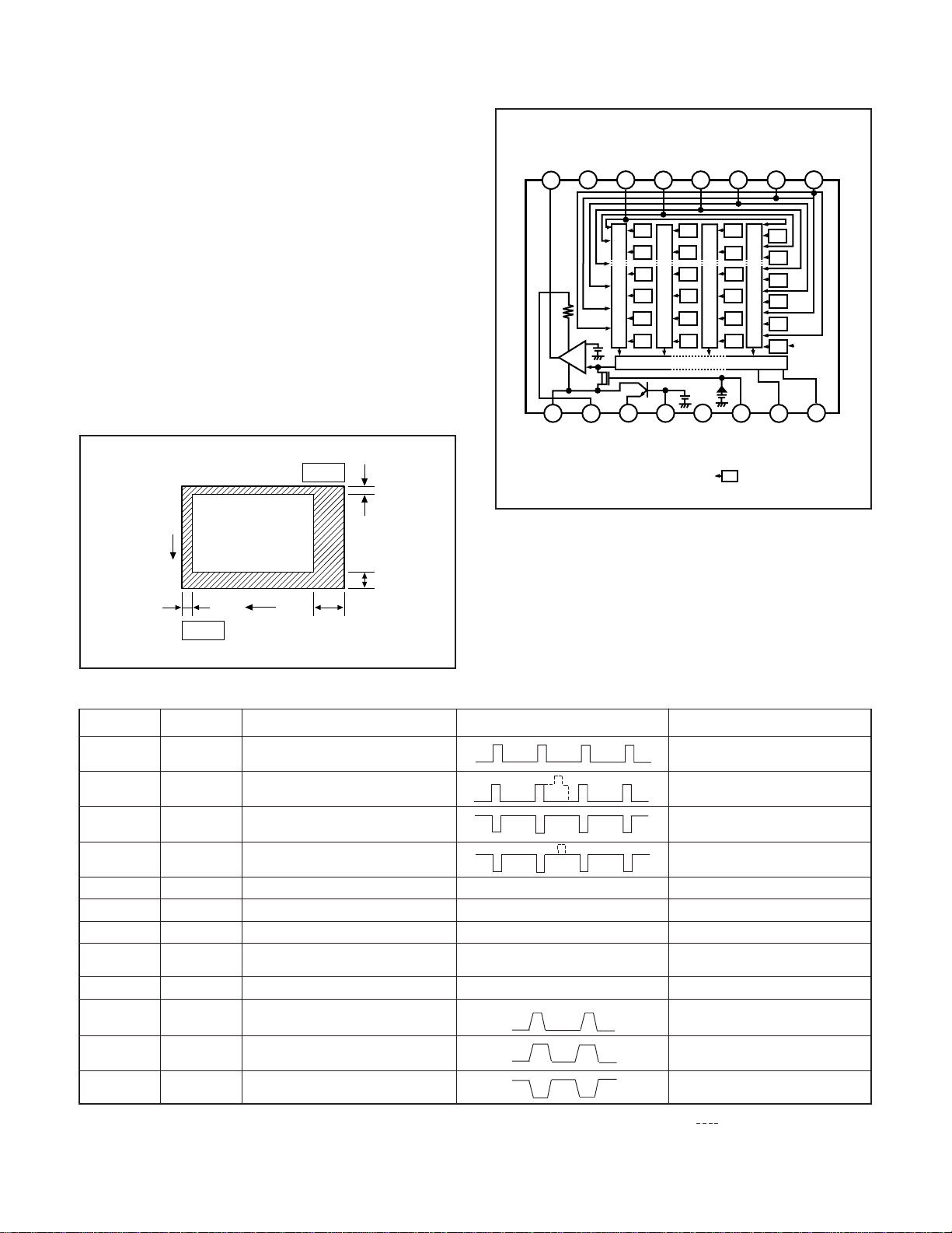
1. IC Configuration
IC903 (RJ23J1AA0AT) CCD imager
IC902 (74VHC04MTC) H driver
IC904 (LR366854) V driver
IC905 (AD9802) CDS, AGC, A/D converter
φ3B
Vφ3A
Vφ2
Vφ1B
Vφ1A
GND
VOUT
7
6
8
5
3
4
2
Vφ4
V
1
2. IC903 (CCD)
[Structure]
Interline type CCD image sensor
Optical size 1/2.7 inch format
Effective pixels 1292 (H) ×966 (V)
Pixels in total 1344 (H) ×971 (V)
Optical black
Horizontal (H) direction: Front 3 pixels, Rear 49 pixels
Vertical (V) direction: Front 2 pixels, Rear 3 pixels
Dummy bit number Horizontal : 28 Vertical : 2
Pin 1
2
V
3
3
Pin 9
H
49
Cy
Mg
Cy
Mg
Cy
Mg
13
φRG
Ye
Ye
Ye
Cy
G
Mg
Cy
G
Mg
Cy
G
Mg
(Note)
15
1
Hφ
16
2
Hφ
14
NC
Ye
G
Ye
G
Ye
Vertical register
G
Horizontal register
11
φSUB
12
L
V
9
10
DD
V
GND
(Note):Photo sensor
Fig. 1-2. CCD Block Diagram
Fig. 1-1.Optical Black Location (Top View)
Pin No.
1
2, 3
4
5, 6
7, 10
8
9
11
12
13
15
16
Symbol
4
V φ
V φ
3B, V φ3A
V φ2
V φ1B, V φ1A
GND
OUT
V
VDD
φSUB
VL
φRG
H φ
1
H φ2
Pin Description
Vertical register transfer clock
Vertical register transfer clock
Vertical register transfer clock
Vertical register transfer clock
GND
Signal output
Circuit power
Substrate clock
Protection transistor bias
Reset gate clock
Horizontal register transfer clock
Horizontal register transfer clock
Waveform
GND
DC
DC
DC
Table 1-1. CCD Pin Description
Voltage
-7 V, 0 V
-7 V, 0 V, 13 V
-7 V, 0 V
-7 V, 0 V, 13 V
0 V
Aprox. 6 V
13 V
Aprox. 6 V
(Different from every CCD)
-7V
8 V, 11.5 V
0 V, 3.5 V
0 V, 3.5 V
When sensor read-out
−2 −
Page 3
3. IC902 (H Driver) and IC904 (V Driver)
27
29
36
26
16
22
21
30
2319
11
12
17
PBLK
A/D
ACVDD
CMLEVEL
VRT
VTB
STBY CLPOB
ADCMODE
TIMING
GENERATOR
CLPDM PGACONT1
PGACONT2
SHP
SHD ADCCLK
PIN
DIN
ADCIN
DOUT
DRVDD
DVDD
ADVDD
2
37 20
18
47
48
43
3341
CLAMP
REFERENCE
CLAMP
CDS
PGA
MUX S/H
AD9802
An H driver (IC902) and V driver (IC904) are necessary in
order to generate the clocks (vertical transfer clock, horizontal transfer clock and electronic shutter clock) which driver
the CCD.
IC902 is an inverter IC which drives the horizontal CCDs (H1
and H2). In addition the XV1-XV4 signals which are output
from IC102 are the vertical transfer clocks, and the XSG1
and XSG signal which is output from IC102 is superimposed
onto XV1 and XV3 at IC904 in order to generate a ternary
pulse. In addition, the XSUB signal which is output from IC102
is used as the sweep pulse for the electronic shutter, and the
RG signal which is output from IC102 is the reset gate clock.
14
CC
1A
1Y
2A
2Y
3A
1
2
3
4
5
V
13
6A
12
6Y
11
5A
10
5Y
4. IC905 (CDS, AGC Circuit and A/D Converter)
The video signal which is output from the CCD is input to
Pins (26) and (27) of IC905. There are S/H blocks inside IC905
generated from the XSHP and XSHD pulses, and it is here
that CDS (correlated double sampling) is carried out.
After passing through the CDS circuit, the signal passes
through the AGC amplifier. It is A/C converted internally into
a 10-bit signal, and is then input to IC102 of the CA2 circuit
board. The gain of the AGC amplifier is controlled by the voltage at pin (29) which is output from IC102 of the CA2 circuit
board and smoothed by the PWM.
6
3Y
7
GND
Fig. 1-3. IC902 Block Diagram
VSHT
VMb
VL
V2
V4
NC
V3B
V3A
4A
9
4Y
8
1
2
3
4
5
6
7
8
MIX
MIX
Fig. 1-5. IC905 Block Diagram
24
VOFDH
XSG2B
23
XSUB
22
XV2
21
20
XV1
19
XSG1A
XV3
18
VDD
17
V1B
V1A
VMa
VH
9
10
11
12
MIX
MIX
Fig. 1-4. IC904 Block Diagram
−3 −
16
15
14
13
GND
XSG2A
XV4
XSG1B
Page 4
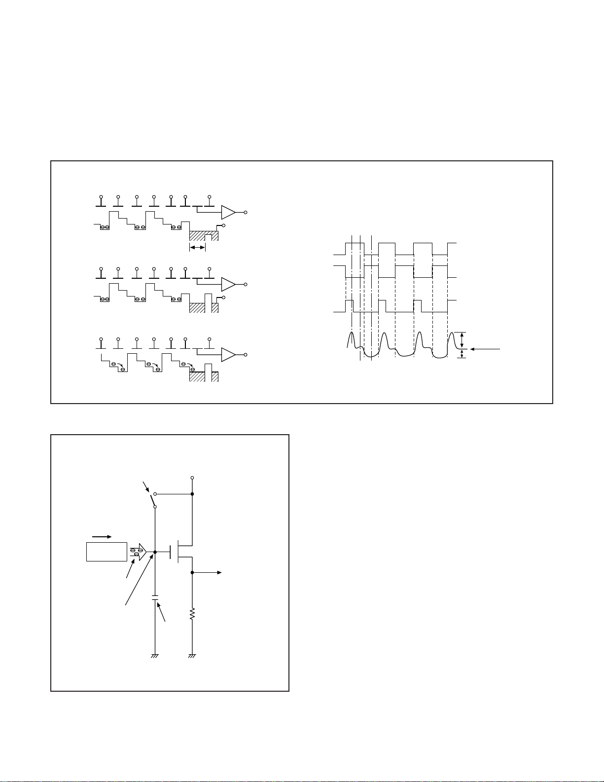
5. Transfer of Electric Charge by the Horizontal CCD
The transfer system for the horizontal CCD emplays a 2-phase drive method.
The electric charges sent to the final stage of the horizontal CCD are transferred to the floating diffusion, as shown in Fig. 1-6.
RG is turned on by the timing in (1), and the floating diffusion is charged to the potential of PD. The RG is turned off by the timing
in (2). In this condition, the floating diffusion is floated at high impedance. The H1 potential becomes shallow by the timing in (3),
and the electric charge now moves to the floating diffusion.
Here, the electric charges are converted into voltages at the rate of V = Q/C by the equivalent capacitance C of the floating
diffusion. RG is then turned on again by the timing in (1) when the H1 potential becomes deep.
Thus, the potential of the floating diffusion changes in proportion to the quantity of transferred electric charge, and becomes
CCD output after being received by the source follower. The equivalent circuit for the output circuit is shown in Fig. 1-7.
(1)
H1 H2 H1 H2 H1 HOG RG
CCD OUT
Floating diffusion
(2)
H1 H2 H1 H2 H1 HOG RG
PD
H1
H2
CCD OUT
PD
RG
(1) (2) (3)
3.5V
0V
3.5V
0V
15.5V
12V
(3)
H1 H2 H1 H2 H1 HOG RG
Reset gate pulse
Direction of transfer
H Register
Electric
charge
Floating diffusion gate is
floated at a high impedance.
CCD OUT
CCD OUT
Fig. 1-6. Horizontal Transfer of CCD Imager and Extraction of Signal Voltage
6. Lens drive block
6-1. Shutter drive
The shutter drive circuit (PCTRL) which is output from the ASIC
expansion port (IC109) is drived the shutter drive circuit, and
then shutter plunger opened and closed.
6-2. Iris and focus drive
The stepping motor drive signal (IN1, IN2 and ENA) for using
both iris and focus which is output from the ASIC expansion
port (IC109) is drived by motor driver (LB1838M). Detection of
the standard motoring positions is carried out by means of the
photointerruptor (PI) inside the lens block.
C is charged
equivalently
13V Pre-charge drain bias (PD)
Voltage output
RG pulse peak signal
Signal voltage
Black level
Fig. 1-7. Theory of Signal Extraction Operation
−4 −
Page 5

1-2. CA2 CIRCUIT DESCRIPTION
1. Circuit Description
1-1. Digital clamp
The optical black section of the CCD extracts averaged values from the subsequent data to make the black level of the
CCD output data uniform for each line. The optical black section of the CCD averaged value for each line is taken as the
sum of the value for the previous line multiplied by the coefficient k and the value for the current line multiplied by the
coefficient 1-k.
1-2. Signal processor
1. γ correction circui t
This circuit performs (gamma) correction in order to maintain
a linear relationship between the light input to the camera
and the light output from the picture screen.
2. Color generation circuit
This circuit converts the CCD data into RGB signals.
3. Matrix circuit
This circuit generates the Y signals, R-Y signals and B-Y signals from the RGB signals.
4. Horizontal and vertical ape rture circuit
This circuit is used gemerate the aperture signal.
1-3. AE/AWB and AF computing circuit
The AE/AWB carries out computation based on a 64-segment screen, and the AF carries out computations based on
a 6-segment screen.
1-4. SDRAM controller
This circuit outputs address, RAS, CAS and AS data for controlling the SDRAM. It also refreshes the SDRAM.
1-5. Communication control
1. UART
The RS-232C can be sued for both synchronous and asynchronous transmission.
2. SIO
This is the interface for the 4-bit microprocessor.
3. PIO/PWM/SIO for LCD
8-bit parallel input and output makes it possible to switch
between individual input/output and PWM input/output.
1-6. TG/SG
Timing generated for 1.3 million/1.09 million pixel CCD control.
1-7. Digital encorder
It generates chroma signal from color difference signal.
2. Outline of Operation
When the shutter opens, the reset signals (ASIC and CPU)
and the serial signals (“take a picture” commands) from the
4-bit microprocessor are input and operation starts. When
the TG/SG drives the CCD, picture data passes through the
A/D and CDS, and is then input to the ASIC as 10-bit data.
The AF, AE, AWB, shutter, and AGC value are computed from
this data, and three exposures are made to obtain the optimum picture. The data which has already been stored in the
SDRAM is read by the CPU and color generation is carried
out. Each pixel is interpolated from the surrounding data as
being either Ye, Cy, Mg and Gr primary color data to produce
R, G and B data. At this time, correction of the lens distortion
which is a characteristic of wide-angle lenses is carried out.
After AWB and γprocessing are carried out, a matrix is gen-
erated and aperture correction is carried out, and the data is
then compressed by the JPEG method by (JPEG) and is then
written to card memory (smart media).
When the data is to be output to an external device, it is taken
data from the memory and output via the UART. When played
back on the LCD and monitor, data is transferred from memery
to the SDRAM, and is displayed over the SDRAM display
area.
3. LCD Block
During monitoring, YUV conversion is carried out for the 10bit CCD data which is input from the A/D conversion block to
the ASIC and is then transferred to the DRAM so that the
CCD data can be displayed on the LCD.
The data which has accumulated in the DRAM is passed
through the NTSC encoder , and after D/A conversion is carried out to change the data into a Y/C signal, the data is sent
to the LCD panel and displayed.
If the shutter button is pressed in this condition, the 10-bit
data which is output from the A/D conversion block of the
CCD is sent to the DRAM (DMA transfer), and after processor, it is displayed on the LCD as a freeze-frame image.
During playback, the JPEG image data which has accumulated in the flash memory is converted to YUV signals, and
then in the same way as during monitoring, it is passed through
the NTSC endoder, and after D/A conversion is carried out to
change the data into a Y/C signal, the data is sent to the LCD
panel and displayed.
The two analog signal (Y/C signals) from the ASIC are converted into RGB signals by the LCD driver, and these RGB
signals and control signal which output from the LCD driver
are used to drive the LCD panel. The RGB signals are 1H
transposed so that no DC component is present in the LCD
element, and the two horizontal shift register clocks drive the
horizontal shift registers inside the LCD panel so that the 1H
transposed RGB signals are applied to the LCD panel. Because the LCD closes more as the difference in potential between the COM (common polar voltage: fixed at DC) and the
R, G and B signals becomes greater, the display becomes
darker; if the difference in potential is smaller, the element
opens and the LCD become brighter.
−5−
Page 6

1-3. PW1 POWER CIRCUIT DESCRIPTION
1. Outline
This is the main power circuit, and is comprised of the following blocks.
Switching controller (IC501)
Digital 5 V and analog system power output (Q5001, T5001)
Digital 3.5 V system power supply (Q5007)
Digital 2.6 V system power output (IC503)
LCD system power supply (Q5008, T5002)
Backlight power supply output (Q5011, T5003)
2. Switching Controller (IC501)
This is the basic circuit which is necessary for controlling the
power supply for a PWM-type switching regulator, and is provided with four built-in channels, only CH1 (digital 5 V, analog
system), CH3 (LCD system), CH2 (digital 3.5 V) and CH4
(backlight) are used. Feedback from 5 V (D) (CH1), 3.2 V (D)
(CH2) , 5.0 V (L) (CH3) and 7.7 V (L) (CH4) power supply
outputs are received, and the PWM duty is varied so that
each one is maintained at the correct voltage setting level.
2-1. Short-circuit protection circuit
If output is short-circuited for the length of time determined
by the condenser which is connected to Pin (17) of IC501, all
output is turned off. The control signal (P ON, P(A) ON and
LCD ON) are recontrolled to restore output.
3. Digital 5 V and Analog System Power Output
5 V (D) , 13 V (A), -7.0 V (A) and 5 V (A) are output. Feedback for the 5 V (D) is provided to the switching controller
(Pins (28) and (29) of IC501) so that PWM control can be
carried out.
4. Digital 3.5 V System Power Output
3.5 V (D) is output. Feedback is provided to the swiching controller (Pin (25) and (26) of IC501) so that PWM control can
be carried out.
5. Digital 2.6 V Power Output
2.6 V (D) is output. 2.6 V (D) can be controled regular voltage
by series regulator IC (IC503).
6. LCD System Power Output
5 V (L) 1, 5 V (L) 2, 7.5 V (L), 13.5 V (L) and -15 V (L) are
output. Feedback for the 5 V (L) is provided to the switching
controller (Pin (11) and (12) of IC501) so that PWM control
can be carried out.
7. Backlight Power Supply output
7.7 V (L) is output. Feedback is sent to pins (7) and (8) of the
switching controller (IC501) for PWM control to be carried
out.
−6−
Page 7

1-4. PW1 STROBE CIRCUIT DESCRIPTION
1. Charging Circuit
When UNREG power is supplied to the charge circuit and the
CHG signal becomes High (3.3 V), the charging circuit starts
operating and the main electorolytic capacitor is charged with
high-voltage direct current.
However, when the CHG signal is Low (0 V), the charging
circuit does not operate.
1-1. Power switch
When the CHG signal switches to Hi, Q5406 turns ON and
the charging circuit starts operating.
1-2. Power supply filter
L5401 and C5401 constitute the power supply filter. They
smooth out ripples in the current which accompany the switching of the oscillation transformer.
1-3. Oscillation circuit
This circuit generates an AC voltage (pulse) in order to increase the UNREG power supply voltage when drops in current occur. This circuit generates a drive pulse with a frequency
of approximately 50-100 kHz. Because self-excited light omission is used, the oscillation frequency changes according to
the drive conditions.
2. Light Emission Circuit
When RDY and TRIG signals are input from the ASIC expansion port, the stroboscope emits light.
2-1. Emission control circuit
When the RDY signal is input to the emission control circuit,
Q5409 switches on and preparation is made to let current
flow to the light emitting element. Moreover, when a STOP
signal is input, the stroboscope stops emitting light.
2-2. Trigger circuit
When a TRIG signal is input to the trigger circuit, D5405
switches on, a high-voltage pulse of several kilovolts is generated inside the trigger circuit, and this pulse is then applied
to the light emitting part.
2-3. Light emitting element
When the high-voltage pulse form the trigger circuit is applied to the light emitting part, currnet flows to the light emitting element and light is emitted.
※ Beware of electric shocks.
1-4. Oscillation transformer
The low-voltage alternating current which is generated by the
oscillation control circuit is converted to a high-voltage alternating current by the oscillation transformer.
1-5. Rectifier circuit
The high-voltage alternating current which is generated at
the secondary side of T5401 is rectified to produce a highvoltage direct current and is accumulated at electrolytic capacitor C5412 on the main circuit board.
1-6. Voltage monitoring circuit
This circuit is used to maintain the voltage accumulated at
C5412 at a constance level.
After the charging voltage is divided and converted to a lower
voltage by R5417 and R5419, it is output to the SY1 circuit
board as the monitoring voltage VMONIT. When this VMONIT
voltage reaches a specified level at the SY1 circuit board, the
CHG signal is switched to Low and charging is interrupted.
−7−
Page 8
1-5. SY1 CIRCUIT DESCRIPTION
1. Configuration and Functions
For the overall configuration of the SY1 circuit board, refer to the block diagram. The configuration of the SY1 circuit board
centers around a 4-bit microprocessor (IC301).
The 4-bit microprocessor handles the following functions.
1. Operation key input, 2. Mode LCD display, 3. Clock control, 4. Power ON/OFF, 5. Storobe charge control
Pin
1
2
3
4
5
6
7
8
9
10
11
12
13
14
15
16
17
18
19
20
21
22
23
24
25
26
27
28
29
30
31
32
33
34~37
38
39~41
42~44
45~47
48~61
62~64
Signal
SCAN OUT3
LCD ON 2
P(A) ON
P ON
CHG ON
ASIC TEST
MAIN RESET
ASIC RESET
STBY (R) LED
STBY (G) LED
SELF LED
LCD ON 1
AD ON
RXD
SCK
SO
SI
S. REQ
DIN CONNECT
BAT OFF
RESET
XIN
XOUT
VSS
VDD
XCOUT
XCIN
AVSS
VREF
BATTERY
CHG VOL
AV JACK
CARD
SCAN IN 0~3
VLC3
NOT USED
COM3~COM1
NOT USED
S14~S1
SCAN OUT 0~2
I/O
O
O
O
O
O
O
O
O
O
O
O
O
O
I
O
O
I
I
I
I
I
I
O
-
-
O
I
I
I
I
I
I
I
I
I
O
O
O
O
O
Table 4-1. 4-bit Microprocessor Port Specification
Key matrix output 3
LCD monitor ON/OFF signal (2) L : ON
DC/DC converter (analog) ON/OFF signal L : ON
DC/DC converter (digital) ON/OFF signal L : ON
Flash charge ON/OFF signal L : ON
ASIC reset control signal
SPARC reset signal L : Reset output
ASIC reset signal L : Reset output
Standby LED (red) ON/OFF signal L : LED light
Standby LED (green) ON/OFF signal L : LED light
Self-timer LED ON/OFF signal L : LED light
LCD monitor ON/OFF signal (1) L : ON
AD converter power ON/OFF signal L : ON
RS-232C RXD input terminal
Serial clock output ( → ASIC)
Serial data output ( → ASIC)
Serial data input ( ← ASIC)
Serial communication request singnal L : Serial request
DIN jack connection detection signal H : Connection
Battery OFF detection signal L : OFF
Reset input
Main clock oscillation terminal (1 MHz)
Main clock oscillation terminal
GND
VDD
Clock oscillation terminal (32.768 kHz)
Clock oscillation terminal
Analog GND input terminal
Analog reference voltage input terminal
Battery voltage input (AD input)
Strobe charge voltage input (AD input)
AV output cable connection detection signal L : Connection
Memory card attachment detection signal L : Attachment
Key matrix input 0~3
Mode LCD power input terminal
-
LCD common output
-
Mode LCD segment output
Key matrix output 0~2
Outline
−8−
Page 9
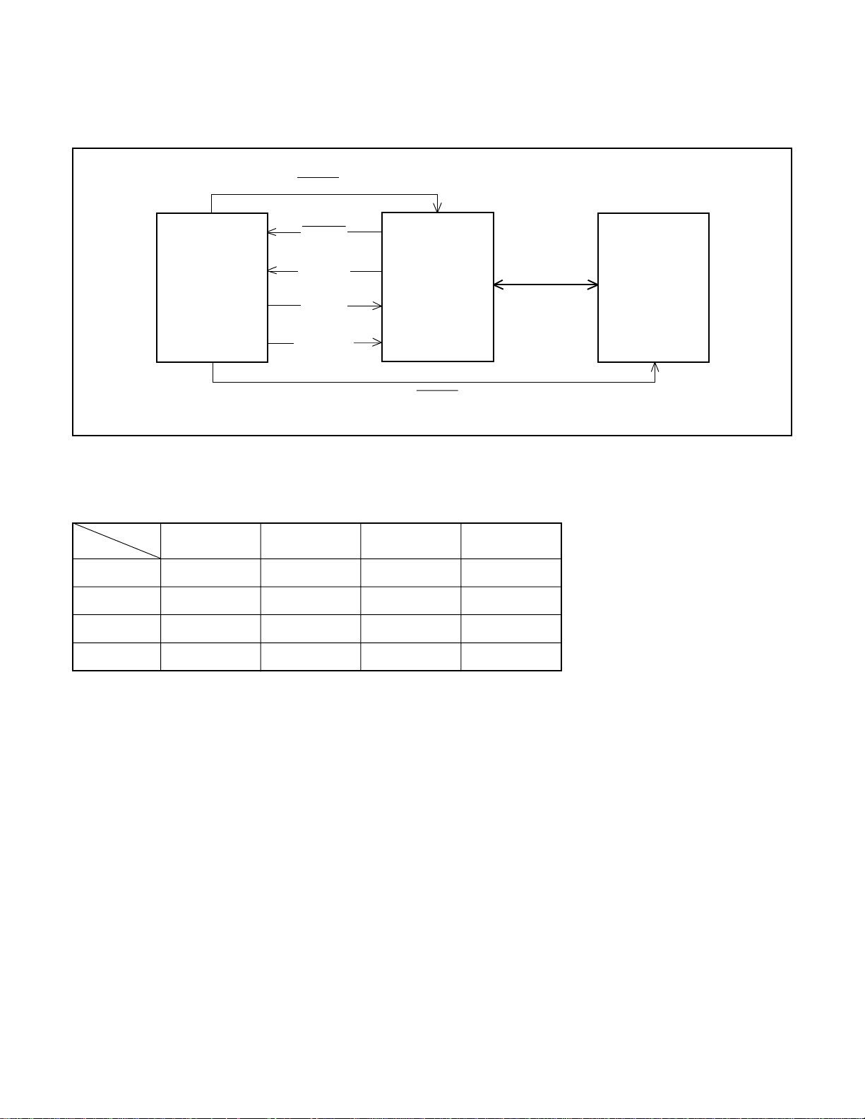
2. Internal Communication Bus
The SY1 circuit board carries out overall control of camera operation by detecting the input from the keyboard and the condition
of the camera circuits. The 4-bit microprocessor reads the signals from each sensor element as input data and outputs this data
to the camera circuits (ASIC) or to the LCD display device as operation mode setting data. Fig. 4-1 shows the internal communication between the 4-bit microprocessor, ASIC and SPARC lite circuits.
RESET
S. REQ
4-bit
Microprocessor
ASIC SO
ASIC SI
ASIC SCK
RESET
Fig. 4-1 Internal Bus Communication System
3. Key Operaiton
For details of the key operation, refer to the instruction manual.
SCAN
SCAN
OUT
IN
0
1
2
3
0
TEST
PLAY/CAMERA
SPECIAL
LENS COVER
BARRIER
1
MODE
SET
+
-
23
CARD LID
FLASH
SHUTTER 2nd
ASIC
DATA BUS
IMAGE
MONITOR
SHUTTER 1st
32-bit
SPARC lite
Table 4-2. Key Operation
−9−
Page 10

4. Power Supply Control
The 4-bit microprocessor controls the power supply for the overall system.
The following is a description of how the power supply is turned on and off. When the battery is attached, a regulated 3.2 V
voltage is normally input to the 4-bit microprocessor (IC301) by IC302, so that clock counting and key scanning is carried out
even when the power switch is turned off, so that the camera can start up again. When the battery is removed, the 4-bit microprocessor operates in sleep mode using the backup capacitor (C3050). At this time, the 4-bit microprocessor only carries out
clock counting, and waits in standby for the battery to be attached again. When a switch is operated, the 4-bit microprocessor
supplies power to the system as required.
The 4-bit microprocessor first sets both the P (A) ON signal at pin (3) and the P ON signal at pin (4) to low, and then turns on the
DC/DC converter. After this, High signals are output from pins (7) and (8) so that the ASIC and the SPARC lite are set to the
active condition. If the LCD monitor is on, the LCD ON 1 signal at pin (12) and the LCD ON 2 signal at pin (2) set to Low, and the
DC/DC converter for the LCD monitor is turned on. Once SPARC lite processing is completed, the ASIC and the SPARC lite
return to the reset condition, all DC/DC converters are turned off and the power supply to the whole system is halted.
Lens
cover
close
Lens
cover
open
Lens cover
open
Power voltage
Power switch OFF
Playback
Power switch ON-
Auto power down
Shutter switch ON
Resolution, Flash,
Self timer switch ON
LCD finder
Power voltage
Power switch OFF
Power switch ON-
Auto power down
SPARC
Lite
3.3 V 3.3 V 5 V
OFF OFF OFF
ON
OFF
ON
OFF OFF OFF
ON
Table 4-3. Camera Mode (Battery Operation)
SPARC
Lite
3.3 V
OFF
OFF
ASIC,
memory
ON ON
OFF OFF
ON ON
ON ON
ASIC,
memory
3.3 V 5 V
OFF OFF
OFF OFF
RS232C
RS232C
driver
Driver
CCD
3.2 V (A)
+12 V -9 V
OFF
OFF
OFF
ON → OFF
OFF
ON
CCD
5 V (A)
+12 V -9 V
OFF
OFF
4bit
CPU
3.2 V
(ALWAYS)
32KHz OFF OFF
1MHz ON ON
1MHz ON OFF
1MHz ON OFF
1MHz ON OFF
1MHz ON ON
4bit
CPU
3.2 V
(ALWAYS)
32 KHz OFF OFF
1 MHz ON OFF
MODE
LCD
3.2 V
(ALWAYS)
MODE
LCD
3.2 V
(ALWAYS)
MONITOR
5V (L)
+12V etc.
MONITOR
5 V (L)
+12V etc.
LCD
LCD
Take a picture
Lens
cover
open
Note) P. SAVE = Power save mode, 1 MHz = Main clock operation, 32 kHz = Sub clock operation
Erase image
Download image
Continuous image
Message from host
ON
ON
ON
ON
ON
Table 4-4. Host Mode (Battery Operation)
ON ON
ON ON
ON ON
ON ON
ON ON
−10−
ON → OFF
OFF
OFF
ON
ON
1 MHz ON OFF
1 MHz ON OFF
1 MHz ON OFF
1 MHz ON OFF
1 MHz ON OFF
Page 11

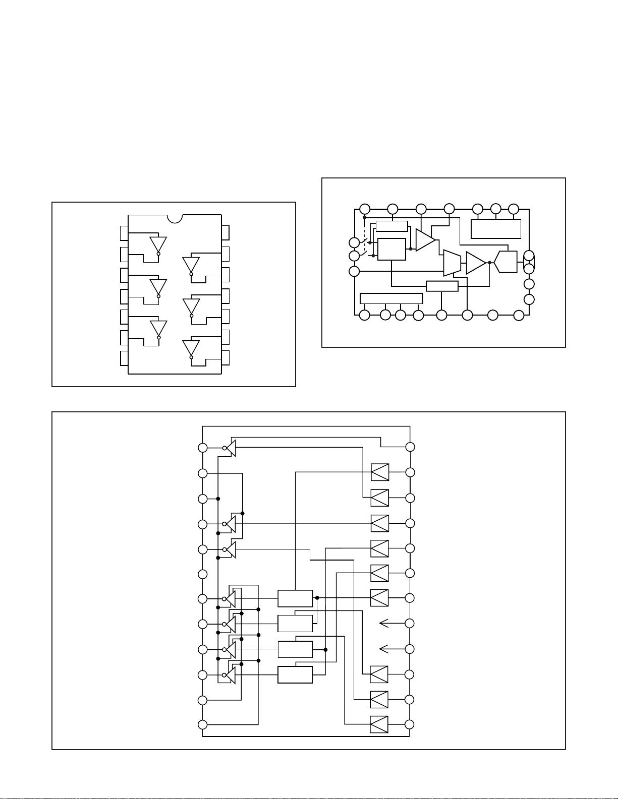
2. DISASSEMBL Y
2-1. REMOV AL OF CABINET FRONT AND CABINET BACK
1. Slide the battery cover, and open it.
4. Screw 2 x 5
7. Cabinet front
3. Holder battery
2. Screw 2 x 5
10. FPC
5. Two screws
2 x 5
8. Back cabinet
9. Connector
5. Screw 2 x 5
6. Open the
cover jack.
5. Three screws
2 x 5
2-2. REMOV AL OF PW1 BOARD AND SY1 BOARD
7. Connector
5. PW1 board
1. Three screws
2 x 5
2. Three connectors
6. Two screws 2 x 5
8. Connector
4. Two connectors
B
6. Screw 2 x 5
9. SY1 board
A
A
3. Terminal board
−11−
Page 12

2-3. REMOV AL OF CA1 BOARD, LCD AND SY2 BOARD
7. Screw 1.7 x 4.5
12. SY2 board
B
9. FPC
11. Screw 1.7 x 4.5
8. Pull it.
6. Two screws
2 x 5
3. FPC
10. LCD
2. Screws
2 x 4
1. Two screws
2 x 6
5. CA1 board
4. Two connectors
6. Screw 2 x 5
2-4. REMOV AL OF LENS VF AND CA2 BOARD
8. CA2 board
6. Housing battery A
5. Screw 2 x 5
7. Housing battery
1. Two screws
2 x 5
2. Lens VF
3. Two screws
2 x 5
4. Holder chassis
−12−
Page 13

2-5. BOARD LOCA TION
SY1 board
CA2 board
CA1 board
SY2 board
PW1 board
−13−
Page 14

3. ELECTRICAL ADJUSTMENT
3-1. Table for Servicing Tools
Ref. No.
J-1
J-2
J-3
J-4
Note: J-1 color viewer is 100 - 110 VAC only.
Color viewer 5,100 K
Siemens star chart
Calibration software
Chart for color adjustment
J-1 J-2
J-3
3-2. Equipment
1. Oscilloscope
2. Digital voltmeter
3. AC adaptor
4. IBM R -compatible PC
5. DC regulated power supply
Name
J-4
Part code
VJ8-0007
VJ8-0166
VJ8-0155
3-3. Adjustment Items and Order
1. IC501 Oscillation Frequency Adjustment
2. 5.1 V (A) Voltage Adjustment
3. 13.5 V (L) Voltage Adjustment
4. Lens Adjustment
5. AWB Adjustment
6. Color Matrix Adjustment
7. CCD Defect Detect Adjustment
8. LCD Panel Adjustment
8-1. LCD H AFC Adjustment
8-2. LCD RGB Offset Adjustment
8-3. LCD Gain Adjustment
8-4. LCD Blue Brightness Adjustment
8-5. LCD Red Brightness Adjustment
8-6. LCD VcomPP Adjustment
8-7. LCD VcomDC Adjustment
Note: If the lens, CCD and board in item 4-7, it is necessary
to adjust again. 4-7 adjustments other than these
should be carried out in sequence.
3-4. Setup
1. System requirements
Windows 95 or 98
IBM R -compatible PC with 486 or higher processor
CD-ROM drive
3.5-inch high-density diskette drive
Serial port with standard RS-232C interface
8 MB RAM
Hard disk drive with at least 15 MB available
VGA or SVGA monitor with at least 256-color display
2. Installing calibration software
1. Insert the calibration software installation diskette into your
diskette drive.
2. Open the explorer.
3. Copy the DSC Cal folder on the floppy disk in the FD drive
to a folder on the hard disk.
3. Color Viewer
Turn on the switch and wait for 30 minutes for aging to take
place before using Color Pure.
4. Computer screen during adjustment
Calibration
AWB
Focus
UV Matrix
Firmware Version:
Upload
Firmware
Image
Initialize
LCD Type
−14−
LCD
R Bright
RGB Offset
Tint
H AFC Test
B Bright
Gain
Phase
VCOMDC
VCOMPP
Page 15

3-5. Connecting the camera to the computer
1. Turn off both camera and computer.
2. Locate the port cover on the side of the camera. Press on the arrows and slide the cover down to open it.
3. Line up the arrow on the cable connector with the notch on the camera's serial port. Insert the connector.
4. Line up the serial connector on the cable with one of the serial ports on your computer, and insert the connector.
5. Turn on the camera and your computer system.
Serial cable
To COM1 or COM2 serial port
AC adaptor
−15−
Page 16

3-6. Adjust Specifications
[PW1 board (Side B)]
VR501
CL534
VR502
4. Lens Adjustment
Serial cable
CL533
CL530
VR503
Note:
1. Voltage adjustment is necessary to repair in the PW1 board
and replace the parts.
Preparation:
1. Remove the shield case at the side A of PW1 board.
2. Terminate pin 1 and pin 2 of S3050 in the SY2 board.
3. Terminate pin 1 and pin 2 of CN303 in the SY1 board.
4. Turn on the monitor switch (S3021) in the SY1 board.
5. Turn on the power.
6. Set the camera mode to the power switch.
1. IC501 Oscillation Frequency Adjustment
Measuring Point
Measuring Equipment
ADJ. Location
ADJ. Value
Adjustment method:
1. Adjust with VR501 to 200 ±0.50 kHz.
CL520
Frequency counter
VR501
200 ±0.50 kHz
Camera
Approx.
69 cm ±3 cm
Siemens
star chart
Preparation:
POWER switch: ON
Adjustment condition:
More than A3 size siemens star chart
Fluorescent light illumination with no flicker
Illumination above the subject should be 400 lux±10 %.
Adjustment method:
1. Set the siemens star chart 69 cm ± 3 cm so that it be-
comes center of the screen.
2. Double-click on the DscCalV123b.
3. Click the Focus, and click the Yes.
4. Lens adjustment value will appear on the screen.
5. Click the OK.
5. AWB Adjustment
2. 5.1 V (A) Voltage Adjustment
Measuring Point
Measuring Equipment
ADJ. Location
ADJ. Value
Adjustment method:
1. Adjust with VR502 to 5.10 ±0.05 V.
CL530
Digital voltmeter
VR502
5.10 ±0.05 V
3. 13.5 V (L) Voltage Adjustment
Measuring Point
Measuring Equipment
ADJ. Location
ADJ. Value
Adjustment method:
1.Adjust with VR503 to 13.50 ±0.10 V
CL533, CL534
Digital voltmeter
VR503
13.50 ± 0.10 V
Serial cable
Camera
0 - 18 cm
All white pattern
Color viewer (5,100K)
Preparation:
POWER switch: ON
Adjusting method:
1. When setting the camera in place, set it to an angle so that
nothing appears in any part of the color viewer except the
white section. (Do not enter any light.)
−16−
Page 17

2. Double-click on the DscCalV123b.
3. Click the AWB, and click the Yes.
4. AWB adjustment value will appear on the screen.
5. Click the OK.
6. Color Matrix Adjustment
Serial cable
8-1. LCD H AFC Adjustment
Preparation:
POWER switch: ON
Adjusting method:
1. Double-click on the DscCalV123b.
2. Select LCD3 on the “LCD Type”.
3. Select 0 on the LCD “H AFC”.
4. While watching the LCD monitor, adjust LCD “H AFC” so
that the edge of the LCD adjustment frame are the same
distance from the left and right edge of the LCD screen.
(A = B)
LCD
LCD screen
A
adjustment
B
frame
Camera
15 cm ± 1 cm
All white pattern color
viewer (5,100K) and
color matrix adjustment chart
Preparation:
POWER switch: ON
Adjustment method:
1. Set the color adjustment chart to the color viewer.
(Do not enter any light.)
2. Set the siemens star chart so that it becomes center of
the screen.
3. Double-click on the DscCalV123b.
4. Click the UV Matrix, and Click the Yes.
5. Color matrix adjustment value will appear on the screen.
6. Click the OK.
7. CCD Defect Detect Adjustment
Adjustment method:
1. Double-click on the DscCalV123b.
2. Select CCD Defect on the LCD “Test”, and click the “Yes”.
3. After adjustment, adjustment value will appear on the screen.
8. LCD Panel Adjustment
[CA2 board (Side B)]
FPC
8-2. LCD RGB Offset Adjustment
Adjusting method:
1. Adjust LCD “RGB offset” so that the amplitude of the CL403
waveform is 3.40 V ± 0.10 Vp-p.
3.40V
±0.10Vp-p
CL403 waveform
8-3. LCD Gain Adjustment
Adjusting method:
1. Adjust LCD “Gain” so that the amplitude of the CL403 wave-
form is 1.85 V ± 0.10 Vp-p.
Note:
8-2. LCD RGB Offset adjustment should always be carried
out first.
CL402
CL420
CL403
CL404
1.85V
±0.10Vp-p
CL403 waveform
−17−
Page 18

8-4. LCD Blue Brightness Adjustment
Adjusting method:
1. Adjust LCD “B Bright” so that the amplitude of the CL404
waveform is VG ± 0.05 Vp-p with respect to the CL403 (VG)
waveform.
Note:
8-2. LCD RGB Offset adjustment and 8-3. LCD Gain adjustment should always be carried out first.
VG
CL403 waveform
VG
CL403 waveform
(VG – 0.1)
± 0.05 Vp-p
CL402 waveform
VG ±
0.05 Vp-p
CL404 waveform
8-5. LCD Red Brightness Adjustment
Adjusting method:
1. Adjust LCD “R Bright” so that the amplitude of the CL402
waveform is (VG – 0.1) ± 0.05 Vp-p with respect to the CL403
(VG) waveform.
Note:
8-2. LCD RGB Offset adjustment and 8-3. LCD Gain adjustment should always be carried out first.
8-6. LCD VcomPP Adjustment
Adjusting method:
1. Adjust LCD“VCOMPP” so that the amplitude of the CL420
waveform is 5.40 V ± 0.25 Vp-p.
5.40V
±0.25Vp-p
CL420 waveform
8-7. LCD VcomDC Adjustment
Adjusting method:
1. Select BLACK on the LCD “Test”.
2. Adjust LCD“VCOMDC” so that the amplitude of the CL420
waveform is -1.10 V ± 0.05 Vp-p with respect to the CL403
(VG) waveform.
−18−
VG waveform
Vcom waveform
VG center level
-1.10V
±0.05Vp-p
Vcom center level
Page 19

4. TROUBLESHOOTING GUIDE
POWER LOSS INOPERTIVE
BARRIER SW
OPEN
IC301-34 (SCAN IN 0)
PULSE INPUT
YES
IC302-7 (UNREG)
HIGH
IC301-25
(VDD)
HIGH
IC301-21
(RESET)
HIGH
IC301-20
(BAT OFF)
HIGH
IC301-23
OSCILLATION
YES
IC301-26
OSCILLATION
YES
CLOSED
NO
CHECK POWER SW,
CN303, R3020, D3014
LOW
LOW
LOW
CHECK IC302, R3051
LOW
NO
R3008, C3003, C3004
NO
R3004, C3001, C3002
BARRIER SW ON
CHECK ST1, CA2
CHECK IC302
CHECK R3052
CHECK X3001,
CHECK X3002,
NORMAL
TAKING INOPERATIVE
PUSH SUTTER
BUTTON
IC301-36, 37
(SCAN IN 2, 3)
PULSE INPUT
YES
CN305-8, 11
(P ON, P(A) ON)
HIGH
IC301-6, 7, 8
HIGH
YES
SERIAL
COMMUNICATION
OK
CHECK CA2
NO
LOW
Q3005, Q3006, ST1
NO
NG
CHECK S3029,
R3022, R3023,
D3015, D3016
CHECK IC301,
CHECK
IC301, CA2, ST1
CHECK IC301,
R3015, R3032,
Q3003, CA2
CHECK IC301
NO PICTURE
CLK (60MHz)
INPUT TO
IC102-18 (CLK IN)
NO
CLK (30 MHz)
INPUT TO
IC101-154 (XTAL 1)
OK
IC102-113 (ZAS)
OK
IC101-68
(ZBREQ)
OK
IC102-111
(ZBGRNT)
OK
IC101-141, 142
(IRL1, 2)
OK
CHECK SOLDERING OF
EACH CPU, ASIC AND
MEMORY PIN
MAIN CLOCK FOR SYSTEM OPERATION
YES
NO OPERATION IF ABSENT
CHECK X1001 OSCILLATOR AND IC111
NG
BASIC CPU BLOCK
CHECK ASIC PIN 22
ALWAYS APPEARS WHEN CPU, ETC. IS ACCESSED
NG
CHECK IF CPU IS READKING PROGRAM, AND
CHECK ADDRESS AND DATA BUS OF IC121
REQUEST FOR USE OF DATA BUS FROM
NG
ASIC TO CPU NO DMA TRANSMISSION IF ABSENT
CHECK IC102-110
RECEIVES ZBREQ SIGNAL AND GIVES PERMISSION
NG
TO ASIC FOR USE OF DATA BUS
NO DMA TRANSMISSION IF ABSENT / CHECK IC101-70
INCORRECT HANDSHAKING BETWEEN 4-BIT
NG
CPU AND RS-232C
CHECK EACH INTERFACE
−19−
FOCUS INOPERATIVE
AFTER LENS ADJ.
THE LENS IS IN
FOCUS
NG
CHECK IC911
OK
CHECK CN903
OK
CHECK LENS
OK
NG
NG
NORMAL
CHECK IC102-107
(PPCS)
CHECK IC908,
Q9072, Q9073
Page 20

3. PARTS LIST
CABINET & CHASSIS PARTS 1
1 636 051 3198 HOLDER BOTTOM-SR5/J
2 636 055 9899 ASSY,CABI FRONT-SR813/E
3 636 056 0093 KNOB LCD ON/OFF-SR813/E
4 636 048 5020 SPRING COMP RELEASE-25/UO
5 636 051 7578 BUTTON SHUTTER-SR46/U
6 636 050 5568 SLIDE FB-SR46/U
7 636 055 7772 KNOB POWER-SR813/E
8 636 050 5537 LEVER LENS A-SR46/U
9 636 050 5414 COVER LENS-SR46/U
10 636 050 5452 DEC SELF TIMER-SR46/U
11 636 051 1293 SPRING KNOB-SR46/U
12 636 052 0035 ASSY,HOLDER LENS-SR46/U
13 645 025 1252 SWITCH,LEAF 1P-1T
14 636 056 1939 ASSY,WIRE SR813E (N.S.P.)
15 636 050 5445 DEC FLASH-SR46/U
16 636 056 7757 COMPL,COVER BATTERY-813/E
17 636 051 3280 SHAFT COVER CARD-SR5/J
18 636 051 3174 COVER CARD-SR5/J
101
LOCATION PARTS NO. DESCRIPTIONLOCATION PARTS NO. DESCRIPTION
19 636 051 4959 COVER PLATE-SR5/J
20 636 051 8285 COVER JACK-SR46/EX
21 636 049 5968 STAND-SR4/J, STAND
22 636 056 0147 SPACER MONITOR-SR813/E
23 636 051 3204 HOLDER KNOB MONITOR-SR5/J
24 636 049 9270 ASSY,FLEXIBLE PWB,MODE SW
25 636 049 5869 HOLDER GLIP-SR4/J
26 636 049 5975 SHAFT STRAP-SR4/J
27 636 055 9912 ASSY,CABI BACK-SR813/E
28 636 051 3259 KNOB MONITOR-SR5/J
29 636 050 4936 SPACER MODE-SR4/J
30 636 051 5819 BUTTON MODE-SR5/U
31 636 051 7684 TERMINAL BOAD-SR46/EX
32 636 050 5872 LABEL CAUTION BATT-SR4/J
33 636 057 2485 SPACER FLASH-SR813/E
101 411 171 8700 SCR S-TPG PAN 2X5
102 411 174 8103 SCR S-TPG PAN PCS 2X3.5
103 411 173 3000 SCR S-TPG PAN PCS 2X4
104 411 170 8602 SCR S-TPG PAN 2X5
105 411 171 7109 SCR S-TPG PAN PCS 2X2.5
N.S.P.: Not available as service parts.
26
27
28
30
29
25
32
15
103
31
24
101
105
14
33
(N.S.P.)
23
5
4
6
7
13
103
102
22
102
101
21
105
101
19
101
20
8
11
3
9
102
12
18
17
10
16
2
101
SR813/E PartsList1
103
104
1
20
Page 21

CABINET & CHASSIS PARTS 2
1 636 055 7949 COMPL PWB,PW-1
2 636 049 5845 HOLDER CHASSIS-SR4/J
3 636 055 9387 COMPL,REFLECTOR
4 636 051 3211 HOUSING BATTERY A-SR5/J
5 636 055 7871 COMPL PWB,CA-2 ,EXCEPT VPC-Z380
5 636 055 7895 COMPL PWB,CA-2 ,VPC-Z380 ONLY
6 636 051 3228 HOUSING BATTERY B-SR5/J
7 645 028 1440 LENS(ASSY)
8 636 056 2615 ADHESIVE TAPE VF-SR661/J
9 636 051 7653 REFLECTOR SY1-SR46/U
10 645 028 1457 ASSY,LENS,VF
11 636 051 9275 SPACER VF-SR5/J
N.S.P.: Not available as service parts.
104
LOCATION PARTS NO. DESCRIPTIONLOCATION PARTS NO. DESCRIPTION
12 645 028 0474 OPTICAL FILTER
13 636 052 0172 SPACER,SXGA
14 409 460 0207 IC RJ23J1AA0AT
15 636 048 2296 MOUNTING,LENS
16 636 048 2319 SPACER,INSULATOR
17 636 055 7918 COMPL PWB,CA-1
18 636 055 7925 COMPL PWB,SY-1
19 636 055 7765 HOLDER MONITOR-SR813/E
20 636 055 7932 COMPL PWB,SY-2
21 645 037 5071 LCD
104 411 170 8602 SCR S-TPG PAN 2X5
106 411 173 7008 SCR S-TPG PAN PCS 1.7X4.5
107 411 022 7807 SCR S-TPG PAN 2X6
108 411 002 4901 SCR PAN 2X4
21
104
106
18
19
108
106
20
6
104
107
5
4
16 17
15
14
13
12
104
3
104
7
104
9
104
104
104
SR813/E PartsList2
104
8
10
2
11
1
21
Page 22

ELECTRICAL PARTS
Note:
1. Materials of Capacitors and Resistors are abbreviated as follows ;
Resistors Capacitors
MT-FILM Metallized Film Resistor MT-POLYEST Metallized Polyester Capacitor
MT-GLAZE Metallized Glaze Resistor MT-COMPO Metallized Composite Capacitor
OXIDE-MT Oxide Metallized Film Resistor TA-SOLD Tantalum Solid Capacitor
AL-SOLID Aluminum Solid Capacitor
NP-ELECT Non-Polarized Electrolytic Capacitor
OS-SOLID Aluminum Solid Capacitors with Organic
2. Tolerance of Capacitor (10pF over) and Resistor are noted with follow symboles.
DL-ELECT Double Layered Electrolytic Capacitor
F ............1% G ............2% J ............5% K ............10%
M ..........20% N ..........30% Z ..........+80% ~ -20%
3. Capacitors
µ
F P : pF
U :
4. Inductors
µ
H MH : mH
UH :
5. N.S.P. : Not available as service parts.
LOCATION PARTS NO. DESCRIPTION LOCATION PARTS NO. DESCRIPTION
COMPL PWB,CA-1
636 055 7918
(SEMICONDUCTORS)
Q9001 405 079 6203 TR 2SC4399-4
OR 405 079 6302 TR 2SC4399-5
Q9002 405 102 5609 TR 2SD1819A-R
OR 405 092 4101 TR 2SC4081-R
Q9004 405 102 5609 TR 2SD1819A-R
OR 405 092 4101 TR 2SC4081-R
Q9015 405 129 2308 TR UMZ1N
OR 405 106 4806 TR XP4601
Q9041 405 133 8907 TR DTC114EUA
OR 405 140 1502 TR DTC123JUA
Q9502 405 047 2602 TR 2SB1124-S
Q9503 405 102 5609 TR 2SD1819A-R
OR 405 092 4101 TR 2SC4081-R
(INTEGRATED CIRCUITS)
IC902 409 392 9101 IC 74VHC04MTC
IC904 409 432 2000 IC LR366854
IC905 409 418 9702 IC AD9802JSTRL
IC909 409 407 0505 IC TK11331BM
IC951 409 446 9309 IC NJM2125F
(DIODES)
D9002 407 113 5609 DIODE DSH015
OR 407 134 7200 DIODE MA141K
D9003 407 198 9905 DIODE MA727
(INDUCTORS)
L9002 645 020 1905 INDUCTOR,120 OHM
L9003 645 020 1912 INDUCTOR,240 OHM
(CAPACITORS)
C9001 403 343 8700 CERAMIC 1U M 12V
C9002 403 155 1807 CERAMIC 0.01U K 25V
C9003 403 155 1500 CERAMIC 180P J 50V
C9004 403 338 4403 CERAMIC 0.1U K 16V
C9005 403 343 8700 CERAMIC 1U M 12V
C9006 403 155 1807 CERAMIC 0.01U K 25V
C9007 403 338 4403 CERAMIC 0.1U K 16V
C9009 403 073 1200 CERAMIC 0.033U K 50V
C9010 403 073 1200 CERAMIC 0.033U K 50V
C9012 403 320 5500 CERAMIC 1U Z 25V
C9013 403 155 1807 CERAMIC 0.01U K 25V
C9014 403 172 6106 CERAMIC 270P J 50V
C9016 403 155 1807 CERAMIC 0.01U K 25V
C9017 403 338 4403 CERAMIC 0.1U K 16V
C9018 403 155 1807 CERAMIC 0.01U K 25V
C9019 403 320 5500 CERAMIC 1U Z 25V
C9023 403 320 5302 CERAMIC 0.15U K 25V
C9025 403 338 4403 CERAMIC 0.1U K 16V
C9026 403 338 4403 CERAMIC 0.1U K 16V
C9027 403 338 4403 CERAMIC 0.1U K 16V
C9029 403 338 4403 CERAMIC 0.1U K 16V
C9030 403 345 4304 TA-SOLID 22U M 10V
C9031 403 338 4403 CERAMIC 0.1U K 16V
C9032 403 338 4403 CERAMIC 0.1U K 16V
C9033 403 338 4403 CERAMIC 0.1U K 16V
C9034 403 338 4403 CERAMIC 0.1U K 16V
C9035 403 343 8700 CERAMIC 1U M 12V
C9036 403 155 1807 CERAMIC 0.01U K 25V
C9037 403 343 8700 CERAMIC 1U M 12V
C9038 403 343 8700 CERAMIC 1U M 12V
C9039 403 155 1807 CERAMIC 0.01U K 25V
C9040 403 338 4403 CERAMIC 0.1U K 16V
C9041 403 338 4403 CERAMIC 0.1U K 16V
C9043 403 155 1807 CERAMIC 0.01U K 25V
C9044 403 343 8700 CERAMIC 1U M 12V
C9045 403 343 8700 CERAMIC 1U M 12V
C9046 403 334 8603 ELECT 220U M 6.3V
C9048 403 296 1308 TA-SOLID 10U M 20V
C9051 403 320 5500 CERAMIC 1U Z 25V
C9056 403 343 8700 CERAMIC 1U M 12V
C9058 403 164 0204 CERAMIC 0.1U Z 25V
C9059 403 155 1500 CERAMIC 180P J 50V
C9060 403 155 1500 CERAMIC 180P J 50V
C9061 403 155 1500 CERAMIC 180P J 50V
C9065 403 155 1500 CERAMIC 180P J 50V
C9066 403 155 1500 CERAMIC 180P J 50V
C9067 403 155 1500 CERAMIC 180P J 50V
C9068 403 155 1500 CERAMIC 180P J 50V
C9080 403 155 1500 CERAMIC 180P J 50V
C9100 403 338 4403 CERAMIC 0.1U K 16V
C9510 403 164 0204 CERAMIC 0.1U Z 25V
C9511 403 157 4202 CERAMIC 220P J 50V
C9512 403 163 9802 CERAMIC 0.047U Z 25V
C9513 403 345 4304 TA-SOLID 22U M 10V
(RESISTORS)
R9001 401 105 7909 MT-GLAZE 0.000 ZA 1/16W
R9003 401 105 8005 MT-GLAZE 1M JA 1/16W
R9004 401 105 4205 MT-GLAZE 33K JA 1/16W
R9005 401 105 0405 MT-GLAZE 100 JA 1/16W
R9006 401 105 5806 MT-GLAZE 56 JA 1/16W
R9011 401 105 7909 MT-GLAZE 0.000 ZA 1/16W
R9012 401 105 7909 MT-GLAZE 0.000 ZA 1/16W
R9013 401 105 7909 MT-GLAZE 0.000 ZA 1/16W
R9014 401 241 3407 MT-GLAZE 5.6K DC 1/16W
R9015 401 241 5302 MT-GLAZE 10K DC 1/16W
R9016 401 105 7909 MT-GLAZE 0.000 ZA 1/16W
R9019 401 105 4106 MT-GALZE 3.3K JA 1/16W
R9021 401 241 3407 MT-GLAZE 5.6K DC 1/16W
R9024 401 177 2604 MT-GLAZE 3.9 JA 1/16W
R9025 401 241 1908 MT-GLAZE 1K DC 1/16W
R9026 401 250 5003 MT-GLAZE 100K DC 1/16W
R9029 401 105 0405 MT-GLAZE 100 JA 1/16W
R9031 401 105 4601 MT-GLAZE 3.9K JA 1/16W
R9032 401 241 3506 MT-GLAZE 82K DC 1/16W
R9033 401 105 6407 MT-GLAZE 68 JA 1/16W
Semiconductive Electrolytic Capacitor
22
Page 23

LOCATION PARTS NO. DESCRIPTION LOCATION PARTS NO. DESCRIPTION
R9034 401 105 0306 MT-GLAZE 10 JA 1/16W
R9035 401 105 0306 MT-GLAZE 10 JA 1/16W
R9036 401 250 5508 MT-GLAZE 47K DC 1/16W
R9037 401 250 5003 MT-GLAZE 100K DC 1/16W
R9038 401 105 8005 MT-GLAZE 1M JA 1/16W
R9039 401 241 5302 MT-GLAZE 10K DC 1/16W
R9041 401 105 7909 MT-GLAZE 0.000 ZA 1/16W
R9042 401 105 7909 MT-GLAZE 0.000 ZA 1/16W
R9043 401 105 7909 MT-GLAZE 0.000 ZA 1/16W
R9062 401 166 7306 MT-FILM 470 DU 1/16W
R9063 401 166 8808 MT-FILM 2.2K DU 1/16W
R9501 401 241 1908 MT-GLAZE 1K DC 1/16W
R9502 401 038 0602 MT-GLAZE 220 JA 1/10W
R9503 401 241 1908 MT-GLAZE 1K DC 1/16W
R9504 401 241 5302 MT-GLAZE 10K DC 1/16W
R9505 401 241 5302 MT-GLAZE 10K DC 1/16W
R9506 401 241 5807 MT-GLAZE 22K DC 1/16W
R9507 401 241 5302 MT-GLAZE 10K DC 1/16W
(CONNECTORS)
CN901 645 018 4413 SOCKET,22P (N.S.P)
CN902 645 018 4413 SOCKET,22P (N.S.P)
CN903 645 002 2876 PLUG,2P (N.S.P)
CN951 645 002 6461 SOCKET,FFC 10P (N.S.P)
COMPL PWB,CA-2
636 055 7871 EXCEPT VPC-Z380
636 055 7895 VPC-Z380 ONLY
(SEMICONDUCTORS)
Q1001 405 115 6907 TR DTC114EE
Q1002 405 120 6008 TR 2SB1197K-R
Q1301 405 131 0200 TR DTC144EUA
OR 405 102 5005 TR UN5213
Q1302 405 131 3607 TR DTA144EUA
OR 405 102 3605 TR UN5113
Q1501 405 129 2100 TR UMT1N
Q1502 405 129 2100 TR UMT1N
Q1503 405 129 2100 TR UMT1N
Q1504 405 129 2308 TR UMZ1N
OR 405 106 4806 TR XP4601
Q1507 405 131 0200 TR DTC144EUA
OR 405 102 5005 TR UN5213
Q1601 405 133 8907 TR DTC114EUA
Q1602 405 102 6705 TR 2SA1745-7
OR 405 102 8303 TR 2SA1745-6
Q1701 405 102 5609 TR 2SD1819A-R
OR 405 092 4101 TR 2SC4081-R
Q1751 405 131 0200 TR DTC144EUA
OR 405 102 5005 TR UN5213
(INTEGRATED CIRCUITS)
IC101 409 420 8502 IC MB86833PMT-GBND
IC102 410 349 7804 IC KS5H8U1160CBP
IC103 409 469 6309 IC HY57V16160DTC-8
OR 409 432 6206 IC UPD4516161AG5A10B9NF
IC109 409 435 7002 IC SN74LV273AP
IC111 409 417 9208 IC W42C27-41G
IC121 409 470 9801 IC 25200813D,EXCEPT VPC-Z380
IC121 409 470 9900 IC 25201813C,VPC-Z380 ONLY
IC131 409 412 4109 IC ADM3202ARU
IC141 409 435 6906 IC SN74LV245AP
IC144 409 407 0703 IC PST9128NR
IC152 409 427 4101 IC TK15405M
IC171 409 433 0401 IC IR3Y29B4
IC172 409 407 0604 IC TK11348BM
IC174 409 445 5500 IC MB88347PFV-G-BND
IC175 409 382 8305 IC NJM3414AV
IC176 409 167 7103 IC NJM2107F
IC177 409 301 5507 IC TC7S08FU
(DIODES)
D1001 407 210 5403 DIODE RB551V-30
D1301 407 149 0807 DIODE 1SS355
D1502 407 109 4609 DIODE MA728
D1601 407 134 7408 DIODE MA141WK
OR 407 130 4401 DIODE DAN202U
D1701 407 166 0606 DIODE MA365
D1901 407 149 0807 DIODE 1SS355
X1101 645 037 0021 OSC,CRYSTAL 14.31818MHZ,VPC-Z380 ONLY
X1101 645 037 0045 OSC,CRYSTAL 17.734475MHZ,
X1701 645 025 6004 OSC,CRYSTAL 3.579545MHZ,VPC-Z380 ONLY
X1701 645 030 0431 OSC,CRYSTAL 4.433619MHZ,EXCEPT VPC-Z380
L1001 645 016 0349 INDUCTOR,600 OHM
L1002 645 016 0349 INDUCTOR,600 OHM
L1073 645 020 1899 INDUCTOR,68 OHM
L1107 645 020 1899 INDUCTOR,68 OHM
L1301 645 020 2070 INDUCTOR,750 OHM
L1302 645 020 2087 INDUCTOR,1500 OHM
L1501 645 021 1737 INDUCTOR,47U J
L1502 645 021 1706 INDUCTOR,33U J
L1505 645 020 2087 INDUCTOR,1500 OHM
L1510 645 021 1607 INDUCTOR,10U J
L1702 645 021 1607 INDUCTOR,10U J
L1703 645 021 1676 INDUCTOR,27U J
C1001 403 164 0204 CERAMIC 0.1U Z 25V
C1002 403 164 0204 CERAMIC 0.1U Z 25V
C1003 403 164 0204 CERAMIC 0.1U Z 25V
C1004 403 164 0204 CERAMIC 0.1U Z 25V
C1005 403 164 0204 CERAMIC 0.1U Z 25V
C1006 403 164 0204 CERAMIC 0.1U Z 25V
C1007 403 164 0204 CERAMIC 0.1U Z 25V
C1008 403 164 0204 CERAMIC 0.1U Z 25V
C1009 403 164 0204 CERAMIC 0.1U Z 25V
C1010 403 164 0204 CERAMIC 0.1U Z 25V
C1011 403 164 0204 CERAMIC 0.1U Z 25V
C1012 403 164 0204 CERAMIC 0.1U Z 25V
C1013 403 164 0204 CERAMIC 0.1U Z 25V
C1030 403 164 0204 CERAMIC 0.1U Z 25V
C1031 403 164 0204 CERAMIC 0.1U Z 25V
C1033 403 164 0204 CERAMIC 0.1U Z 25V
C1034 403 164 0204 CERAMIC 0.1U Z 25V
C1035 403 164 0204 CERAMIC 0.1U Z 25V
C1036 403 164 0204 CERAMIC 0.1U Z 25V
C1038 403 164 0204 CERAMIC 0.1U Z 25V
C1039 403 164 0204 CERAMIC 0.1U Z 25V
C1040 403 157 2901 CERAMIC 47P J 50V
C1041 403 164 0204 CERAMIC 0.1U Z 25V
C1042 403 164 0204 CERAMIC 0.1U Z 25V
C1043 403 164 0204 CERAMIC 0.1U Z 25V
C1044 403 164 0204 CERAMIC 0.1U Z 25V
C1045 403 164 0204 CERAMIC 0.1U Z 25V
C1046 403 164 0204 CERAMIC 0.1U Z 25V
C1047 403 164 0204 CERAMIC 0.1U Z 25V
C1048 403 164 0204 CERAMIC 0.1U Z 25V
C1049 403 164 0204 CERAMIC 0.1U Z 25V
C1050 403 164 0204 CERAMIC 0.1U Z 25V
C1051 403 164 0204 CERAMIC 0.1U Z 25V
C1052 403 164 0204 CERAMIC 0.1U Z 25V
C1053 403 157 3304 CERAMIC 68P J 50V
C1054 403 157 3304 CERAMIC 68P J 50V
C1055 403 155 1609 CERAMIC 33P J 50V
C1061 403 164 0204 CERAMIC 0.1U Z 25V
C1062 403 164 0204 CERAMIC 0.1U Z 25V
C1063 403 164 0204 CERAMIC 0.1U Z 25V
C1070 403 207 0307 CERAMIC 1U Z 16V
C1101 403 332 9503 CERAMIC 1U M 6.3V
C1102 403 155 1807 CERAMIC 0.01U K 25V
C1104 403 323 6306 CERAMIC 0.1U K 16V
C1105 403 157 1904 CERAMIC 10P D 50V
C1201 403 207 0307 CERAMIC 1U Z 16V
C1301 403 164 0204 CERAMIC 0.1U Z 25V
C1302 403 164 0204 CERAMIC 0.1U Z 25V
C1303 403 164 0204 CERAMIC 0.1U Z 25V
C1304 403 164 0204 CERAMIC 0.1U Z 25V
C1305 403 164 0204 CERAMIC 0.1U Z 25V
C1401 403 164 0204 CERAMIC 0.1U Z 25V
C1403 403 314 8104 TA-SOLID 33U M 6.3V
C1404 403 164 0204 CERAMIC 0.1U Z 25V
C1501 403 322 3504 CERAMIC 22U Z 10V
C1503 403 322 3504 CERAMIC 22U Z 10V
C1504 403 164 0204 CERAMIC 0.1U Z 25V
C1506 403 283 6309 CERAMIC 1U Z 10V
(CRYSTAL DEVICES)
EXCEPT VPC-Z380
(INDUCTORS)
(CAPACITORS)
23
Page 24

LOCATION PARTS NO. DESCRIPTION LOCATION PARTS NO. DESCRIPTION
C1507 403 207 0307 CERAMIC 1U Z 16V
C1508 403 155 1609 CERAMIC 33P J 50V,EXCEPT VPC-Z380
C1508 403 157 3106 CERAMIC 56P J 50V,VPC-Z380 ONLY
C1509 403 164 0204 CERAMIC 0.1U Z 25V
C1510 403 192 5905 CERAMIC 0.1U K 25V
C1511 403 207 0307 CERAMIC 1U Z 16V
C1512 403 314 8104 TA-SOLID 33U M 6.3V
C1513 403 314 8104 TA-SOLID 33U M 6.3V
C1514 403 323 6207 CERAMIC 1U K 10V
C1515 403 155 1500 CERAMIC 180P J 50V,VPC-Z380 ONLY
C1515 403 157 3809 CERAMIC 120P J 50V,EXCEPT VPC-Z380
C1601 403 207 0307 CERAMIC 1U Z 16V
C1701 403 323 6207 CERAMIC 1U K 10V
C1702 403 155 1807 CERAMIC 0.01U K 25V
C1703 403 164 0204 CERAMIC 0.1U Z 25V
C1704 403 275 3002 CERAMIC 0.047U K 16V
C1705 403 348 9108 CERAMIC 0.47U K 6.3V
C1706 403 314 5905 CERAMIC 0.47U K 16V
C1707 403 155 1807 CERAMIC 0.01U K 25V
C1708 403 323 6207 CERAMIC 1U K 10V
C1709 403 157 1706 CERAMIC 8P D 50V
C1710 403 332 8209 CERAMIC 10U M 16V
C1711 403 130 4106 CERAMIC 0.068U K 25V
C1712 403 130 4106 CERAMIC 0.068U K 25V
C1713 403 130 4106 CERAMIC 0.068U K 25V
C1715 403 157 7302 CERAMIC 6800P K 50V
C1716 403 323 6207 CERAMIC 1U K 10V
C1717 403 155 1807 CERAMIC 0.01U K 25V
C1718 403 323 6207 CERAMIC 1U K 10V
C1719 403 332 8209 CERAMIC 10U M 16V
C1720 403 164 0204 CERAMIC 0.1U Z 25V
C1721 403 070 2606 CERAMIC 0.1U Z 50V
C1722 403 323 6207 CERAMIC 1U K 10V
C1723 403 164 0204 CERAMIC 0.1U Z 25V
C1724 403 323 6207 CERAMIC 1U K 10V
C1728 403 164 0204 CERAMIC 0.1U Z 25V
C1732 403 164 0204 CERAMIC 0.1U Z 25V
C1733 403 164 0204 CERAMIC 0.1U Z 25V
C1740 403 164 0204 CERAMIC 0.1U Z 25V
C1741 403 164 0204 CERAMIC 0.1U Z 25V
C1742 403 164 0204 CERAMIC 0.1U Z 25V
C1743 403 164 0204 CERAMIC 0.1U Z 25V
C1744 403 155 1807 CERAMIC 0.01U K 25V
C1748 403 283 6309 CERAMIC 1U Z 10V
C1751 403 155 1807 CERAMIC 0.01U K 25V
C1752 403 207 0307 CERAMIC 1U Z 16V
C1753 403 332 8209 CERAMIC 10U M 16V
C1754 403 155 1807 CERAMIC 0.01U K 25V
C1761 403 155 1807 CERAMIC 0.01U K 25V
C1770 403 215 1303 CERAMIC 560P J 50V
C1771 403 164 0204 CERAMIC 0.1U Z 25V
C1772 403 164 0204 CERAMIC 0.1U Z 25V
C1773 403 157 4202 CERAMIC 220P J 50V
C1774 403 069 1702 CERAMIC 1000P K 50V
C1775 403 298 9609 CERAMIC 0.1U K 16V
C1776 403 155 1302 CERAMIC 150P J 50V
C1777 403 215 1303 CERAMIC 560P J 50V
C1792 403 283 6309 CERAMIC 1U Z 10V
C1793 403 283 6309 CERAMIC 1U Z 10V
C1794 403 341 4803 CERAMIC 10U K 10V
C1901 403 175 4604 ELECT 220U M 4V
C1902 403 210 6402 TA-SOLID 10U M 16V
C1903 403 210 6402 TA-SOLID 10U M 16V
C1904 403 113 3805 CERAMIC 1000P K 50V
C1905 403 113 3805 CERAMIC 1000P K 50V
C1906 403 113 3805 CERAMIC 1000P K 50V
(RESISTOR PACKS)
RB101 645 001 3201 R-NETWORK 100KX4 0.063W
RB102 645 001 3201 R-NETWORK 100KX4 0.063W
RB103 645 001 3201 R-NETWORK 100KX4 0.063W
RB104 645 001 3201 R-NETWORK 100KX4 0.063W
(RESISTORS)
R1001 401 105 0603 MT-GLAZE 10K JA 1/16W
R1002 401 105 0603 MT-GLAZE 10K JA 1/16W
R1003 401 105 0603 MT-GLAZE 10K JA 1/16W
R1004 401 105 2706 MT-GLAZE 220 JA 1/16W
R1005 401 105 8104 MT-GLAZE 56K JA 1/16W
R1006 401 105 0702 MT-GLAZE 100K JA 1/16W
R1030 401 105 2706 MT-GLAZE 220 JA 1/16W
R1031 401 105 7206 MT-GLAZE 82 JA 1/16W
R1033 401 105 3901 MT-GLAZE 33 JA 1/16W
R1035 401 105 3901 MT-GLAZE 33 JA 1/16W
R1036 401 105 2706 MT-GLAZE 220 JA 1/16W
R1037 401 105 2706 MT-GLAZE 220 JA 1/16W
R1038 401 105 2706 MT-GLAZE 220 JA 1/16W
R1039 401 105 7206 MT-GLAZE 82 JA 1/16W
R1041 401 105 7206 MT-GLAZE 82 JA 1/16W
R1042 401 105 0603 MT-GLAZE 10K JA 1/16W
R1043 401 105 0603 MT-GLAZE 10K JA 1/16W
R1044 401 105 7909 MT-GLAZE 0.000 ZA 1/16W
R1045 401 105 4502 MT-GLAZE 390 JA 1/16W
R1046 401 105 0405 MT-GLAZE 100 JA 1/16W
R1047 401 105 7909 MT-GLAZE 0.000 ZA 1/16W
R1048 401 105 0603 MT-GLAZE 10K JA 1/16W
R1049 401 105 0603 MT-GLAZE 10K JA 1/16W
R1051 401 105 0603 MT-GLAZE 10K JA 1/16W
R1053 401 105 2706 MT-GLAZE 220 JA 1/16W
R1054 401 105 2706 MT-GLAZE 220 JA 1/16W
R1055 401 105 2706 MT-GLAZE 220 JA 1/16W
R1056 401 105 2706 MT-GLAZE 220 JA 1/16W
R1057 401 105 2706 MT-GLAZE 220 JA 1/16W
R1058 401 105 2706 MT-GLAZE 220 JA 1/16W
R1059 401 105 2706 MT-GLAZE 220 JA 1/16W
R1061 401 105 2706 MT-GLAZE 220 JA 1/16W
R1101 401 105 7909 MT-GLAZE 0.000 ZA 1/16W,VPC-Z380 ONLY
R1101 401 105 0504 MT-GLAZE 1K JA 1/16W,EXCEPT VPC-Z380
R1102 401 105 0306 MT-GLAZE 10 JA 1/16W
R1103 401 105 7909 MT-GLAZE 0.000 ZA 1/16W,EXCEPT VPC-Z380
R1105 401 105 0405 MT-GLAZE 100 JA 1/16W,VPC-Z380 ONLY
R1105 401 105 7909 MT-GLAZE 0.000 ZA 1/16W,EXCEPT VPC-Z380
R1106 401 105 7909 MT-GLAZE 0.000 ZA 1/16W
R1201 401 105 0306 MT-GLAZE 10 JA 1/16W
R1302 401 105 7909 MT-GLAZE 0.000 ZA 1/16W
R1303 401 105 7909 MT-GLAZE 0.000 ZA 1/16W
R1304 401 105 0504 MT-GLAZE 1K JA 1/16W
R1305 401 105 0603 MT-GLAZE 10K JA 1/16W
R1306 401 105 0603 MT-GLAZE 10K JA 1/16W
R1308 401 105 5400 MT-GLAZE 47K JA 1/16W
R1401 401 105 7909 MT-GLAZE 0.000 ZA 1/16W
R1402 401 105 0603 MT-GLAZE 10K JA 1/16W
R1403 401 105 7909 MT-GLAZE 0.000 ZA 1/16W
R1405 401 105 7909 MT-GLAZE 0.000 ZA 1/16W
R1406 401 105 7909 MT-GLAZE 0.000 ZA 1/16W
R1407 401 105 5202 MT-GLAZE 470 JA 1/16W
R1408 401 105 5202 MT-GLAZE 470 JA 1/16W
R1409 401 105 0603 MT-GLAZE 10K JA 1/16W
R1410 401 105 5202 MT-GLAZE 470 JA 1/16W
R1411 401 105 0603 MT-GLAZE 10K JA 1/16W
R1412 401 105 3307 MT-GLAZE 2.7K JA 1/16W
R1413 401 105 5202 MT-GLAZE 470 JA 1/16W
R1414 401 105 3307 MT-GLAZE 2.7K JA 1/16W
R1415 401 105 5202 MT-GLAZE 470 JA 1/16W
R1416 401 105 5202 MT-GLAZE 470 JA 1/16W
R1417 401 105 0603 MT-GLAZE 10K JA 1/16W
R1418 401 105 0603 MT-GLAZE 10K JA 1/16W
R1501 401 166 5708 MT-FILM 100 DU 1/16W
R1502 401 166 5500 MT-FILM 82 DC 1/16W
R1503 401 105 1501 MT-GLAZE 1.5K JA 1/16W
R1504 401 166 7504 MT-FILM 560 DU 1/16W
R1505 401 166 8907 MT-FILM 2.4K DU 1/16W
R1506 401 166 8105 MT-FILM 1K DU 1/16W
R1507 401 166 5302 MT-FILM 68 DC 1/16W
R1508 401 166 5906 MT-FILM 120 DU 1/16W
R1509 401 105 5905 MT-GLAZE 560 JA 1/16W
R1510 401 105 1501 MT-GLAZE 1.5K JA 1/16W
R1511 401 105 7909 MT-GLAZE 0.000 ZA 1/16W
R1512 401 105 1501 MT-GLAZE 1.5K JA 1/16W
R1513 401 105 1501 MT-GLAZE 1.5K JA 1/16W
R1514 401 105 1501 MT-GLAZE 1.5K JA 1/16W
R1515 401 105 1501 MT-GLAZE 1.5K JA 1/16W
R1518 401 166 7108 MT-FILM 390 DU 1/16W
R1519 401 105 6506 MT-GLAZE 680 JA 1/16W
R1520 401 166 8303 MT-FILM 1.2K DU 1/16W
R1521 401 166 7108 MT-FILM 390 DU 1/16W
R1522 401 105 1501 MT-GLAZE 1.5K JA 1/16W
R1523 401 105 5806 MT-GLAZE 56 JA 1/16W
24
Page 25

LOCATION PARTS NO. DESCRIPTION LOCATION PARTS NO. DESCRIPTION
R1524 401 105 7909 MT-GLAZE 0.000 ZA 1/16W
R1525 401 105 0603 MT-GLAZE 10K JA 1/16W
R1526 401 166 5302 MT-FILM 68 DC 1/16W
R1527 401 105 0504 MT-GLAZE 1K JA 1/16W
R1602 401 105 0504 MT-GLAZE 1K JA 1/16W
R1603 401 105 7305 MT-GLAZE 820 JA 1/16W
R1604 401 105 5301 MT-GLAZE 4.7K JA 1/16W
R1605 401 105 5301 MT-GLAZE 4.7K JA 1/16W
R1607 401 105 2706 MT-GLAZE 220 JA 1/16W
R1608 401 105 0603 MT-GLAZE 10K JA 1/16W
R1611 401 105 0603 MT-GLAZE 10K JA 1/16W
R1612 401 105 0603 MT-GLAZE 10K JA 1/16W
R1701 401 105 2904 MT-GLAZE 22K JA 1/16W
R1702 401 105 8005 MT-GLAZE 1M JA 1/16W
R1703 401 105 6001 MT-GLAZE 5.6K JA 1/16W
R1704 401 105 7404 MT-GLAZE 8.2K JA 1/16W
R1705 401 105 6506 MT-GLAZE 680 JA 1/16W
R1706 401 105 4205 MT-GLAZE 33K JA 1/16W
R1709 401 105 0405 MT-GLAZE 100 JA 1/16W
R1710 401 167 3505 MT-FILM 270K DD 1/16W
R1711 401 167 1907 MT-FILM 56K DD 1/16W
R1714 401 105 5905 MT-GLAZE 560 JA 1/16W
R1715 401 105 5905 MT-GLAZE 560 JA 1/16W
R1718 401 105 5400 MT-GLAZE 47K JA 1/16W
R1719 401 167 0900 MT-FILM 18K DU 1/16W
R1720 401 105 0405 MT-GLAZE 100 JA 1/16W
R1721 401 105 0405 MT-GLAZE 100 JA 1/16W
R1725 401 167 2508 MT-FILM 100K DD 1/16W
R1726 401 167 1402 MT-FILM 33K DU 1/16W
R1727 401 167 1709 MT-FILM 47K DD 1/16W
R1729 401 105 7909 MT-GLAZE 0.000 ZA 1/16W
R1730 401 105 0405 MT-GLAZE 100 JA 1/16W
R1731 401 105 5806 MT-GLAZE 56 JA 1/16W
R1732 401 105 0702 MT-GLAZE 100K JA 1/16W
R1740 401 105 7909 MT-GLAZE 0.000 ZA 1/16W
R1741 401 105 7909 MT-GLAZE 0.000 ZA 1/16W
R1742 401 105 7909 MT-GLAZE 0.000 ZA 1/16W
R1743 401 105 7909 MT-GLAZE 0.000 ZA 1/16W
R1745 401 105 7909 MT-GLAZE 0.000 ZA 1/16W
R1746 401 105 2805 MT-GLAZE 2.2K JA 1/16W
R1747 401 167 1709 MT-FILM 47K DD 1/16W
R1748 401 167 0900 MT-FILM 18K DU 1/16W
R1749 401 167 1600 MT-FILM 43K DD 1/16W
R1750 401 166 3209 MT-FILM 39K DD 1/16W
R1751 401 105 7909 MT-GLAZE 0.000 ZA 1/16W
R1752 401 105 0504 MT-GLAZE 1K JA 1/16W
R1753 401 105 0504 MT-GLAZE 1K JA 1/16W
R1754 401 105 0504 MT-GLAZE 1K JA 1/16W
R1755 401 105 2805 MT-GLAZE 2.2K JA 1/16W
R1756 401 105 0306 MT-GLAZE 10 JA 1/16W
R1757 401 105 7909 MT-GLAZE 0.000 ZA 1/16W
R1758 401 167 1709 MT-FILM 47K DD 1/16W
R1759 401 105 3406 MT-GLAZE 27K JA 1/16W
R1760 401 105 5400 MT-GLAZE 47K JA 1/16W
R1761 401 167 1303 MT-FILM 30K DU 1/16W
R1770 401 105 5400 MT-GLAZE 47K JA 1/16W
R1771 401 105 2904 MT-GLAZE 22K JA 1/16W
R1772 401 105 5301 MT-GLAZE 4.7K JA 1/16W
R1773 401 105 5301 MT-GLAZE 4.7K JA 1/16W
R1774 401 105 8203 MT-GLAZE 68K JA 1/16W
R1775 401 105 8203 MT-GLAZE 68K JA 1/16W
R1776 401 105 8005 MT-GLAZE 1M JA 1/16W
R1777 401 166 6309 MT-FILM 180 DU 1/16W
R1778 401 105 4106 MT-GALZE 3.3K JA 1/16W
R1779 401 105 0603 MT-GLAZE 10K JA 1/16W
R1780 401 105 5301 MT-GLAZE 4.7K JA 1/16W
R1781 401 166 7108 MT-FILM 390 DU 1/16W
R1782 401 167 2102 MT-FILM 68K DD 1/16W
R1783 401 166 3100 MT-FILM 22K DU 1/16W
R1901 401 105 0603 MT-GLAZE 10K JA 1/16W
R1903 401 105 0603 MT-GLAZE 10K JA 1/16W
R1904 401 105 0603 MT-GLAZE 10K JA 1/16W
R1905 401 105 0603 MT-GLAZE 10K JA 1/16W
R1906 401 105 0603 MT-GLAZE 10K JA 1/16W
(JACK)
JK151 645 026 5471 JACK,PHONE D3.6 , VIDEO JACK
(CONNECTORS)
CN101 645 021 9818 PLUG,22P (N.S.P)
CN102 645 021 9818 PLUG,22P (N.S.P)
CN103 645 021 6992 PLUG,16P (N.S.P)
CN104 645 021 6992 PLUG,16P (N.S.P)
CN106 645 025 5571 PLUG,22P (N.S.P)
CN141 645 024 0706 SOCKET,CARD 22P (N.S.P)
CN171 645 037 3947 SOCKET,FPC 26P (N.S.P)
(MISCELLANEOUS)
Y1001 636 051 3235 HOUSING CARD-SR5/J
Y1002 636 051 5048 SPACER SHIELD CA2 SIDE-B
Y1003 411 174 1708 SCR S-TPG PAN PCS 1.7X3.5 (SMART MEDIA)
Y1005 636 056 1960 SPACER CA2 SR813
Y1006 411 174 1708 SCR S-TPG PAN PCS 1.7X3.5 (HOUSING CARD)
COMPL PWB,PW-1
636 055 7949
(SEMICONDUCTORS)
Q5001 405 150 5002 TR CPH3109
Q5002 405 092 1209 TR 2SA1577-Q
OR 405 092 1407 TR 2SA1577-R
Q5003 405 115 5207 TR 2SC4617 R
Q5004 405 129 8409 TR UMC2N
Q5005 405 092 1209 TR 2SA1577-Q
OR 405 092 1407 TR 2SA1577-R
Q5006 405 129 2902 TR UMH11N
Q5007 405 124 5502 TR FP106
Q5008 405 150 5002 TR CPH3109
Q5010 405 129 2308 TR UMZ1N
OR 405 106 4806 TR XP4601
Q5011 405 150 6900 TR CPH3215
Q5012 405 008 7707 TR 2SB815-B7
OR 405 008 7509 TR 2SB815-B6
OR 405 120 6008 TR 2SB1197K-R
Q5013 405 115 6907 TR DTC114EE
Q5014 405 047 3807 TR 2SC3647-S
OR 405 047 3906 TR 2SC3647-T
Q5015 405 047 3807 TR 2SC3647-S
OR 405 047 3906 TR 2SC3647-T
Q5016 405 129 2308 TR UMZ1N
OR 405 106 4806 TR XP4601
Q5017 405 115 5207 TR 2SC4617 R
Q5018 405 092 1209 TR 2SA1577-Q
OR 405 092 1407 TR 2SA1577-R
Q5021 405 115 5207 TR 2SC4617 R
Q5022 405 115 6402 TR DTA114YE
Q5023 405 129 8409 TR UMC2N
Q5024 405 115 6907 TR DTC114EE
Q5026 405 092 1209 TR 2SA1577-Q
OR 405 092 1407 TR 2SA1577-R
Q5027 405 115 6907 TR DTC114EE
Q5401 405 115 7508 TR DTC123JE
Q5402 405 115 6907 TR DTC114EE
Q5405 405 147 9709 TR CPH3205
Q5406 405 150 5002 TR CPH3109
Q5407 405 115 5207 TR 2SC4617 R
Q5409 405 151 9504 TR CY20AAJ-8
(INTEGRATED CIRCUITS)
IC501 409 418 1201 IC BA9737KV
IC502 409 320 9203 IC TA75S01F
IC503 409 461 0701 IC TK11326BM
(DIODES)
D5001 407 201 2701 DIODE RB051L-40
D5002 407 201 2701 DIODE RB051L-40
D5003 407 203 5809 DIODE F02J9
D5004 407 203 5809 DIODE F02J9
D5005 407 210 5403 DIODE RB551V-30
D5007 407 203 5809 DIODE F02J9
D5008 407 203 5809 DIODE F02J9
D5009 407 210 5403 DIODE RB551V-30
D5010 407 210 5403 DIODE RB551V-30
D5011 407 203 5809 DIODE F02J9
D5012 407 210 5403 DIODE RB551V-30
D5402 407 202 0300 DIODE F1F16
D5403 407 122 2606 DIODE SFPM-64
D5404 407 202 0102 DIODE F1SN4
D5405 407 199 4503 DIODE CR08AS-8-T1
25
Page 26

LOCATION PARTS NO. DESCRIPTION LOCATION PARTS NO. DESCRIPTION
D5407 407 151 4701 DIODE 1SS301-(TE85L)
OR 407 130 4401 DIODE DAN202U
OR 407 134 7408 DIODE MA141WK
D5410 407 151 4701 DIODE 1SS301-(TE85L)
OR 407 130 4401 DIODE DAN202U
OR 407 134 7408 DIODE MA141WK
(VARIABLE RESISTORS)
VR501 645 019 5150 VR,SEMI,10K S
VR502 645 019 5143 VR,SEMI,1K S
VR503 645 019 5143 VR,SEMI,1K S
(INDUCTORS)
L5001 645 030 5887 INDUCTOR,1000 OHM
L5002 645 030 5887 INDUCTOR,1000 OHM
L5003 645 033 8762 INDUCTOR,47U K
L5004 645 033 8762 INDUCTOR,47U K
L5005 645 033 8762 INDUCTOR,47U K
L5006 645 033 8663 INDUCTOR,10U K
L5007 645 021 1409 INDUCTOR,47U L
L5008 645 033 8762 INDUCTOR,47U K
L5009 645 033 8762 INDUCTOR,47U K
L5010 645 033 8762 INDUCTOR,47U K
L5011 645 037 0632 INDUCTOR,47U M
L5012 645 037 0717 INDUCTOR,100U M
L5013 645 020 1868 INDUCTOR,750 OHM
L5015 645 020 1868 INDUCTOR,750 OHM
L5016 645 020 1868 INDUCTOR,750 OHM
L5018 645 021 5315 INDUCTOR,110 OHM
L5019 645 033 8762 INDUCTOR,47U K
L5020 645 033 8663 INDUCTOR,10U K
L5021 645 020 1868 INDUCTOR,750 OHM
L5401 645 031 5787 INDUCTOR,15U M
(TRANSFORMERS)
T5001 645 034 7764 TRANS,POWER,PULSE
T5002 645 037 6399 TRANS,POWER,PULSE
T5003 645 036 4228 TRANS,POWER,PULSE
T5401 645 032 8817 TRANS,STEP UP
T5402 645 031 6951 TRANS,STEP UP
(CAPACITORS)
C5001 403 338 4403 CERAMIC 0.1U K 16V
C5002 403 155 1807 CERAMIC 0.01U K 25V
C5003 403 338 4403 CERAMIC 0.1U K 16V
C5004 403 155 1807 CERAMIC 0.01U K 25V
C5005 403 157 4202 CERAMIC 220P J 50V
C5006 403 343 8700 CERAMIC 1U M 12V
C5007 403 343 8700 CERAMIC 1U M 12V
C5008 403 338 4403 CERAMIC 0.1U K 16V
C5009 403 338 4403 CERAMIC 0.1U K 16V
C5010 403 155 1807 CERAMIC 0.01U K 25V
C5011 403 338 4403 CERAMIC 0.1U K 16V
C5012 403 157 3601 CERAMIC 100P J 50V
C5013 403 215 1006 CERAMIC 470P J 50V
C5014 403 343 8700 CERAMIC 1U M 12V
C5015 403 157 3106 CERAMIC 56P J 50V
C5016 403 215 1006 CERAMIC 470P J 50V
C5017 403 157 3601 CERAMIC 100P J 50V
C5018 403 215 1006 CERAMIC 470P J 50V
C5019 403 343 8700 CERAMIC 1U M 12V
C5022 403 345 3109 POS-SOLID 33U M 10V
C5023 403 343 8700 CERAMIC 1U M 12V
C5024 403 325 7608 CERAMIC 1U K 16V
C5025 403 332 8209 CERAMIC 10U M 16V
C5026 403 343 8700 CERAMIC 1U M 12V
C5027 403 333 3708 CERAMIC 10U M 10V
C5028 403 333 3708 CERAMIC 10U M 10V
C5029 403 113 4109 CERAMIC 2200P K 50V
C5030 403 323 9406 TA-SOLID 10U M 10V
C5031 403 323 9406 TA-SOLID 10U M 10V
C5032 403 343 8700 CERAMIC 1U M 12V
C5033 403 334 8603 ELECT 220U M 6.3V
C5034 403 113 4109 CERAMIC 2200P K 50V
C5036 403 333 3708 CERAMIC 10U M 10V
C5037 403 343 8700 CERAMIC 1U M 12V
C5038 403 325 7608 CERAMIC 1U K 16V
C5039 403 325 7608 CERAMIC 1U K 16V
C5042 403 325 7608 CERAMIC 1U K 16V
C5043 403 325 7608 CERAMIC 1U K 16V
C5044 403 333 3708 CERAMIC 10U M 10V
C5045 403 155 2309 CERAMIC 4700P K 50V
C5046 403 323 9406 TA-SOLID 10U M 10V
C5047 403 157 3601 CERAMIC 100P J 50V
C5048 403 343 8700 CERAMIC 1U M 12V
C5050 403 333 3708 CERAMIC 10U M 10V
C5051 403 155 2309 CERAMIC 4700P K 50V
C5052 403 348 4509 ELECT 100U M 16V
C5053 403 325 1101 MT-PPS-FILM 6800P J 50V
C5055 403 325 1200 CERAMIC 12P J 3.15K
C5057 403 155 1500 CERAMIC 180P J 50V
C5058 403 155 1500 CERAMIC 180P J 50V
C5059 403 338 4403 CERAMIC 0.1U K 16V
C5060 403 155 1807 CERAMIC 0.01U K 25V
C5061 403 325 7608 CERAMIC 1U K 16V
C5062 403 155 1807 CERAMIC 0.01U K 25V
C5063 403 215 1006 CERAMIC 470P J 50V
C5071 403 325 7608 CERAMIC 1U K 16V
C5075 403 323 9406 TA-SOLID 10U M 10V
C5076 403 333 3708 CERAMIC 10U M 10V
C5078 403 338 4403 CERAMIC 0.1U K 16V
C5079 403 325 7608 CERAMIC 1U K 16V
C5080 403 343 8700 CERAMIC 1U M 12V
C5081 403 333 3708 CERAMIC 10U M 10V
C5082 403 325 7608 CERAMIC 1U K 16V
C5083 403 323 9406 TA-SOLID 10U M 10V
C5084 403 345 3901 CERAMIC 3.3U M 6.3V
C5085 403 345 3901 CERAMIC 3.3U M 6.3V
C5086 403 345 3901 CERAMIC 3.3U M 6.3V
C5087 403 343 8700 CERAMIC 1U M 12V
C5088 403 323 9406 TA-SOLID 10U M 10V
C5089 403 325 7608 CERAMIC 1U K 16V
C5401 403 345 3109 POS-SOLID 33U M 10V
C5403 403 192 5905 CERAMIC 0.1U K 25V
C5404 403 113 3805 CERAMIC 1000P K 50V
C5406 403 343 8700 CERAMIC 1U M 12V
C5407 403 157 7302 CERAMIC 6800P K 50V
C5409 403 163 9604 CERAMIC 0.033U Z 25V
C5410 403 333 3906 CERAMIC 0.047U M 350V
C5411 403 330 5903 CERAMIC 0.01U K 500V
C5412 404 075 1205 ELECT 60U - 330V
C5414 403 113 3805 CERAMIC 1000P K 50V
(RESISTORS)
R5001 401 105 7909 MT-GLAZE 0.000 ZA 1/16W
R5002 401 250 5003 MT-GLAZE 100K DC 1/16W
R5003 401 250 6208 MT-GLAZE 270K DC 1/16W
R5004 401 105 8005 MT-GLAZE 1M JA 1/16W
R5005 401 105 7909 MT-GLAZE 0.000 ZA 1/16W
R5006 401 250 5003 MT-GLAZE 100K DC 1/16W
R5007 401 250 6208 MT-GLAZE 270K DC 1/16W
R5008 401 105 7909 MT-GLAZE 0.000 ZA 1/16W
R5009 401 105 8005 MT-GLAZE 1M JA 1/16W
R5010 401 105 7909 MT-GLAZE 0.000 ZA 1/16W
R5011 401 241 1908 MT-GLAZE 1K DC 1/16W
R5012 401 250 5508 MT-GLAZE 47K DC 1/16W
R5013 401 241 1908 MT-GLAZE 1K DC 1/16W
R5015 401 250 5805 MT-GLAZE 150K DC 1/16W
R5016 401 105 7909 MT-GLAZE 0.000 ZA 1/16W
R5017 401 105 8005 MT-GLAZE 1M JA 1/16W
R5018 401 105 7909 MT-GLAZE 0.000 ZA 1/16W
R5019 401 105 8005 MT-GLAZE 1M JA 1/16W
R5020 401 250 6208 MT-GLAZE 270K DC 1/16W
R5021 401 250 5805 MT-GLAZE 150K DC 1/16W
R5022 401 241 4909 MT-GLAZE 6.8K DC 1/16W
R5023 401 166 6903 MT-FILM 330 DU 1/16W
R5024 401 241 3407 MT-GLAZE 5.6K DC 1/16W
R5025 401 166 6903 MT-FILM 330 DU 1/16W
R5026 401 241 4909 MT-GLAZE 6.8K DC 1/16W
R5027 401 166 6903 MT-FILM 330 DU 1/16W
R5028 401 241 5302 MT-GLAZE 10K DC 1/16W
R5029 401 250 5003 MT-GLAZE 100K DC 1/16W
R5030 401 250 5003 MT-GLAZE 100K DC 1/16W
R5031 401 250 5003 MT-GLAZE 100K DC 1/16W
R5032 401 241 5609 MT-GLAZE 15K DC 1/16W
R5033 401 241 5708 MT-GLAZE 18K DC 1/16W
R5034 401 241 4909 MT-GLAZE 6.8K DC 1/16W
R5035 401 241 1908 MT-GLAZE 1K DC 1/16W
R5036 401 241 5401 MT-GLAZE 12K DC 1/16W
R5037 401 241 5708 MT-GLAZE 18K DC 1/16W
R5038 401 250 5003 MT-GLAZE 100K DC 1/16W
26
Page 27

LOCATION PARTS NO. DESCRIPTION LOCATION PARTS NO. DESCRIPTION
R5039 401 241 5302 MT-GLAZE 10K DC 1/16W
R5040 401 105 7909 MT-GLAZE 0.000 ZA 1/16W
R5042 401 241 5401 MT-GLAZE 12K DC 1/16W
R5043 401 241 2301 MT-GLAZE 1.8K DC 1/16W
R5044 401 105 7909 MT-GLAZE 0.000 ZA 1/16W
R5046 401 105 4205 MT-GLAZE 33K JA 1/16W
R5047 401 241 3407 MT-GLAZE 5.6K DC 1/16W
R5048 401 241 5609 MT-GLAZE 15K DC 1/16W
R5049 401 241 3407 MT-GLAZE 5.6K DC 1/16W
R5050 401 241 1908 MT-GLAZE 1K DC 1/16W
R5051 401 105 1006 MT-GLAZE 1.2K JA 1/16W
R5053 401 105 3000 MT-GLAZE 220K JA 1/16W
R5054 401 105 6407 MT-GLAZE 68 JA 1/16W
R5055 401 250 5003 MT-GLAZE 100K DC 1/16W
R5056 401 105 1501 MT-GLAZE 1.5K JA 1/16W
R5057 401 250 5508 MT-GLAZE 47K DC 1/16W
R5058 401 241 0505 MT-GLAZE 120 DC 1/16W
R5059 401 241 1908 MT-GLAZE 1K DC 1/16W
R5060 401 113 8004 MT-GLAZE 36K JA 1/16W
R5061 401 241 5807 MT-GLAZE 22K DC 1/16W
R5062 401 241 3407 MT-GLAZE 5.6K DC 1/16W
R5065 401 241 5302 MT-GLAZE 10K DC 1/16W
R5066 401 241 5302 MT-GLAZE 10K DC 1/16W
R5067 401 250 5003 MT-GLAZE 100K DC 1/16W
R5068 401 105 7909 MT-GLAZE 0.000 ZA 1/16W
R5072 401 105 7909 MT-GLAZE 0.000 ZA 1/16W
R5073 401 250 5508 MT-GLAZE 47K DC 1/16W
R5077 401 250 5003 MT-GLAZE 100K DC 1/16W
R5078 401 241 5609 MT-GLAZE 15K DC 1/16W
R5080 401 241 1908 MT-GLAZE 1K DC 1/16W
R5081 401 241 5302 MT-GLAZE 10K DC 1/16W
R5082 401 250 5805 MT-GLAZE 150K DC 1/16W
R5083 401 241 5807 MT-GLAZE 22K DC 1/16W
R5084 401 250 5003 MT-GLAZE 100K DC 1/16W
R5085 401 105 8104 MT-GLAZE 56K JA 1/16W
R5086 401 105 7909 MT-GLAZE 0.000 ZA 1/16W
R5087 401 250 5003 MT-GLAZE 100K DC 1/16W
R5088 401 113 8004 MT-GLAZE 36K JA 1/16W
R5089 401 250 5003 MT-GLAZE 100K DC 1/16W
R5092 401 241 5302 MT-GLAZE 10K DC 1/16W
R5097 401 241 1908 MT-GLAZE 1K DC 1/16W
R5099 401 241 5302 MT-GLAZE 10K DC 1/16W
R5100 401 241 5302 MT-GLAZE 10K DC 1/16W
R5101 401 241 5302 MT-GLAZE 10K DC 1/16W
R5102 401 241 5302 MT-GLAZE 10K DC 1/16W
R5103 401 241 5302 MT-GLAZE 10K DC 1/16W
R5107 401 166 6903 MT-FILM 330 DU 1/16W
R5108 401 241 4909 MT-GLAZE 6.8K DC 1/16W
R5110 401 241 5203 MT-GLAZE 9.1K DC 1/16W
R5111 401 241 0901 MT-GLAZE 270 DC 1/16W
R5401 401 241 1908 MT-GLAZE 1K DC 1/16W
R5408 401 037 3406 MT-GLAZE 82 JA 1/8W
R5409 401 038 6307 MT-GLAZE 470 JA 1/10W
R5410 401 038 5003 MT-GLAZE 390 JA 1/10W
R5411 401 241 5302 MT-GLAZE 10K DC 1/16W
R5412 401 105 1303 MT-GLAZE 15 JA 1/16W
R5413 401 241 5302 MT-GLAZE 10K DC 1/16W
R5414 401 241 1908 MT-GLAZE 1K DC 1/16W
R5417 402 078 4407 MT-GLAZE 10M FKG 1/8W
R5418 401 105 5806 MT-GLAZE 56 JA 1/16W
R5419 401 241 3506 MT-GLAZE 82K DC 1/16W
R5422 402 079 0200 MT-GLAZE 220K JKG 1/8W
R5423 401 105 3901 MT-GLAZE 33 JA 1/16W
R5424 401 105 5806 MT-GLAZE 56 JA 1/16W
R5425 402 077 7409 MT-GLAZE 100K JKG 1/8W
R5426 401 105 5509 MT-GLAZE 470K JA 1/16W
R5429 401 241 5302 MT-GLAZE 10K DC 1/16W
R5467 401 105 7909 MT-GLAZE 0.000 ZA 1/16W
R5470 401 241 3209 MT-GLAZE 4.7K DC 1/16W
(PROTECTORS)
PR501 645 029 2408 PROTECTOR,IC 2A 24V
PR502 645 029 2408 PROTECTOR,IC 2A 24V
(JACKS)
JK501 645 009 0486 SOCKET,DC (DC JACK)
JK502 645 031 0454 JACK,PHONE D2.6
(CONNECTORS)
CN501 645 004 6230 SOCKET,16P (N.S.P)
CN502 645 004 6230 SOCKET,16P (N.S.P)
CN503 645 037 9147 PLUG,SIDE-ZR-SM3 (N.S.P)
CN504 645 005 9445 PLUG,2P (N.S.P)
CN505 645 002 3002 PLUG,2P (N.S.P)
(MISCELLANEOUS)
636 049 9898 SPACER SHEET SR4/U-ST1
636 056 7917 SPACER SHIELD PW1-SR813/E
COMPL PWB,SY-1
636 055 7925
(SEMICONDUCTORS)
Q3001 405 115 5702 TR DTA144EE
Q3002 405 115 5702 TR DTA144EE
Q3003 405 078 6105 TR 2SA1677
OR 405 096 1205 TR DTA124EU
OR 405 119 1007 TR UN5112
Q3004 405 115 5702 TR DTA144EE
Q3005 405 115 5702 TR DTA144EE
Q3006 405 115 5702 TR DTA144EE
Q3008 405 115 7201 TR DTC144EE
Q3009 405 115 5702 TR DTA144EE
(INTEGRATED CIRCUITS)
IC301 410 356 1208 IC M34520M8A-901FP
IC302 409 383 1008 S-8423NFS
(DIODES)
D3001 407 199 1809 LED SML-020MLT, STBY LED
D3002 407 187 6304 LED SML-110VT, SELF TIMER LED
D3003 407 130 2605 DIODE MA143A
D3011 407 162 8507 DIODE DAN222
D3012 407 162 8507 DIODE DAN222
D3013 407 162 8507 DIODE DAN222
D3014 407 162 8507 DIODE DAN222
D3015 407 162 8507 DIODE DAN222
D3016 407 162 8507 DIODE DAN222
D3017 407 162 8507 DIODE DAN222
D3018 407 162 8507 DIODE DAN222
D3019 407 162 8507 DIODE DAN222
D3051 407 149 0807 DIODE 1SS355
(CRYSTAL DEVICES)
X3001 645 012 7649 OSC,CERAMIC 1MHZ
X3002 636 040 1129 OSC CRYSTAL 32.768KHZ
(CAPACITORS)
C3001 403 139 7306 CERAMIC 18P J 50V
C3002 403 139 7306 CERAMIC 18P J 50V
C3003 403 157 3601 CERAMIC 100P J 50V
C3004 403 157 3601 CERAMIC 100P J 50V
C3005 403 155 1807 CERAMIC 0.01U K 25V
C3007 403 325 7608 CERAMIC 1U K 16V
C3008 403 316 1400 CERAMIC 560P J 25V
C3009 403 316 1400 CERAMIC 560P J 25V
C3013 403 113 3805 CERAMIC 1000P K 50V
C3050 403 316 5804 DL-ELECT 0.1F Z 5.5V
C3051 403 274 0903 TA-SOLID 22U M 6.3V
C3052 403 338 4403 CERAMIC 0.1U K 16V
C3053 403 338 4403 CERAMIC 0.1U K 16V
C3054 403 325 7608 CERAMIC 1U K 16V
C3055 403 338 4403 CERAMIC 0.1U K 16V
C3056 403 338 4403 CERAMIC 0.1U K 16V
(RESISTORS)
R3001 401 250 5805 MT-GLAZE 150K DC 1/16W
R3002 401 250 5003 MT-GLAZE 100K DC 1/16W
R3004 401 105 3000 MT-GLAZE 220K JA 1/16W
R3005 401 241 0901 MT-GLAZE 270 DC 1/16W
R3006 401 105 2706 MT-GLAZE 220 JA 1/16W
R3007 401 250 5508 MT-GLAZE 47K DC 1/16W
R3008 401 105 8005 MT-GLAZE 1M JA 1/16W
R3009 401 105 5202 MT-GLAZE 470 JA 1/16W
R3012 401 105 7909 MT-GLAZE 0.000 ZA 1/16W
R3014 401 250 5508 MT-GLAZE 47K DC 1/16W
R3015 401 241 5302 MT-GLAZE 10K DC 1/16W
R3017 401 250 5003 MT-GLAZE 100K DC 1/16W
R3018 401 241 5302 MT-GLAZE 10K DC 1/16W
R3019 401 250 5508 MT-GLAZE 47K DC 1/16W
R3020 401 241 5302 MT-GLAZE 10K DC 1/16W
R3021 401 241 5302 MT-GLAZE 10K DC 1/16W
R3022 401 241 5302 MT-GLAZE 10K DC 1/16W
R3023 401 241 5302 MT-GLAZE 10K DC 1/16W
27
Page 28

LOCATION PARTS NO. DESCRIPTION LOCATION PARTS NO. DESCRIPTION
R3028 401 250 5003 MT-GLAZE 100K DC 1/16W
R3030 401 250 5003 MT-GLAZE 100K DC 1/16W
R3031 401 250 5003 MT-GLAZE 100K DC 1/16W
R3032 401 241 5302 MT-GLAZE 10K DC 1/16W
R3051 401 250 5003 MT-GLAZE 100K DC 1/16W
R3052 401 250 5003 MT-GLAZE 100K DC 1/16W
R3053 401 241 1908 MT-GLAZE 1K DC 1/16W
R3054 401 250 5508 MT-GLAZE 47K DC 1/16W
R3055 401 250 5508 MT-GLAZE 47K DC 1/16W
R3056 401 241 1908 MT-GLAZE 1K DC 1/16W
(SWITCHES)
S3021 645 023 3074 SWITCH,SLIDE 1P-2T, MONITOR ON/OFF
S3029 645 012 7670 SWITCH,PUSH 1P-2T, SHUTTER
(DISPLAY)
A3001 645 026 4368 LCD
(CONNECTORS)
CN301 645 024 8405 SOCKET,22P (N.S.P)
CN302 636 051 8254 ASSY,WIRE SY1&ST1-SR5/J (N.S.P)
CN303 645 025 1320 PLUG,2P (N.S.P)
CN304 645 002 6447 SOCKET,FFC 7P (N.S.P)
CN305 645 002 3002 PLUG,2P (N.S.P)
(MISCELLANEOUS)
636 056 1731 TERMINAL BATTERY C-813/E
636 056 1748 TERMINAL BATTERY D-813/E
PACKING MATERIALS
636 055 9219 CARTON CASE INNER-SR813/E,
VPC-Z380E ONLY
636 056 1793 CARTON CASE INNER-SR813/U,VPC-Z380 ONLY
636 056 1809 CARTON CASE INNER-SR813EX,
VPC-Z380EX ONLY
645 031 3080 POLY SHEET-0300X0300*NC
636 055 9233 REINFORCEMENT PAD,A-813/E
636 055 4627 REINFORCEMENT PAD,B-112/E
COMPL PWB,SY-2
636 055 7932
S3501 645 023 0844 SWITCH,PUSH 1P-1TX1,
CN350 636 055 7741 ASSY,WIRE SY1&TB1-SR813E (N.S.P)
(SWITCH)
(CONNECTORS)
ACCESSORIES
OR 645 025 5403 CABLE,PC DOS/V
OR 645 026 6959 CABLE,VIDEO
645 023 3227 CABLE,PC DOS/V
645 026 1558 CABLE,VIDEO
636 056 4442 CASE SOFT-SR813/E
645 039 6472 DISC,CD-ROM CELIS SR8 WM
(SANYO Software pack)
645 036 9919 DISC,CD-ROM MGI PS8 (Software pack MGI),
EXCEPT VPC-Z380E
636 056 6743 STRAP HAND-SR813/E
636 055 6119 INSTRUCTION MANUAL(CAMERA English) ,
VPC-Z380E ONLY
636 056 1366 INSTRUCTION MANUAL
(CAMERA English,French,Spanish)
,EXCEPT VPC-Z380E
636 056 1649 INSTRUCTION MANUAL
(SANYO software: English)
636 055 5303 INSTRUCTION MANUAL
(MGI: English,French,Spanish,German)
,EXCEPT VPC-Z380E
636 057 0825 INSTRUCTION MANUAL (PDF INSTRUCTION:
English,French,Spanish,German)
Sep./ '99/ 4,760 NS Printed in Japan
SANYO Electric Co., Ltd.
Osaka, Japan
28
Page 29

Sep./ '99/ 4,760 NS Printed in Japan
SANYO Electric Co., Ltd.
Osaka, Japan
Page 30

 Loading...