

Page 1
SERVICE MANUAL
FILE NO.
Color Digital Camera
Contents
1. OUTLINE OF CIRCUIT DESCRIPTION ....................2
2. DISASSEMBLY........................................................12
3. ELECTRICAL ADJUSTMENT..................................15
4. TROUBLESHOOTING GUIDE.................................20
5. PARTS LIST.............................................................21
CABINET AND CHASSIS PARTS 1 ........................21
CABINET AND CHASSIS PARTS 2 ........................22
ELECTRICAL PARTS .............................................. 23
ACCESSORIES .......................................................28
PACKING MATERIALS............................................28
CIRCUIT DIAGRAM (Refer to the separate volume)
VPC-X360E
(Product Code : 126 251 01)
(U.K.)
VPC-X360EX
(Product Code : 126 251 02)
(Europe)
(PAL General)
VPC-X360
(Product Code : 126 251 03)
(U.S.A.)
(Canada)
PRODUCT SAFETY NOTICE
The components designated by a symbol ( ! ) in this schematic diagram designates components whose value are of
special significance to product safety. Should any component designated by a symbol need to be replaced, use only the part
designated in the Parts List. Do not deviate from the resistance, wattage, and voltage ratings shown.
CAUTION : Danger of explosion if battery is incorrectly replaced.
Replace only with the same or equivalent type recommended by the manufacturer.
Discard used batteries according to the manufacturer’s instructions.
NOTE : 1. Parts order must contain model number, part number, and description.
2. Substitute parts may be supplied as the service parts.
3. N. S. P. : Not available as service parts.
Design and specification are subject to change without notice.
SR662/E, EX, U
REFERENCE No. SM5310090
Page 2
1. OUTLINE OF CIRCUIT DESCRIPTION
1-1. CA-1 CIRCUIT DESCRIPTION
1. IC Configuration
IC903 (ICX204AK) CCD imager
IC902 (74VHC04MTC) H driver
IC904 (CXD1267AN) V driver
IC905 (AD9802) CDS/AGC, A/D converter
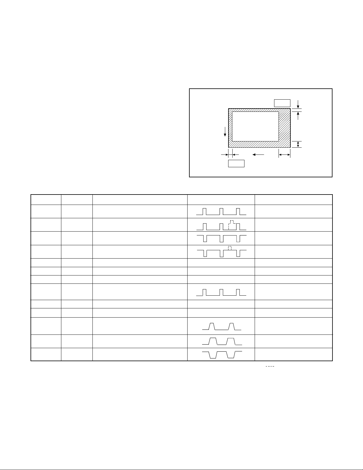
2. IC903 (CCD)
[Structure]
Interline type CCD image sensor
Optical size 1/3 inch format
Effective pixels 1034 (H) ×779 (V)
Pixels in total 1077 (H) ×788 (V)
Chip size 5.80 mm (H) ×4.92 mm (V)
Unit cell size 4.65 μm (H) × 4.65 μ m (H)
Optical black
Horizontal (H) direction: Front 3 pixels, Rear 40 pixels
Vertical (V) direction: Front 7 pixels, Rear 2 pixels
Dummy bit number Horizontal : 29 Vertical : 1
[Features]
Independent storage and retrieval for each pixel
Square pixel unit cell
XGA compatible
R, G, B primary color mosaic filter
Continuous variable speed electronic shutter function
Pin 1
2
V
8
2
Pin 9
H
34
Fig. 1-1.Optical Black Location (Top View)
Pin No.
1
2
3
4
5, 6, 7, 10
8
9
Symbol
V φ
3
V φ
2B
V φ1
V φ2A
GND
OS
OD
Vertical shift register gate clock
Vertical shift register gate clock
Vertical shift register gate clock
Vertical shift register gate clock
GND
Image output
Output transister drain
11 φSUB Board clock
O
12
13
14
15
16
SUB
PL
φRS
φH1
φH2
Board bias
Protection transistor bias
Reset transister gate clock
Horizontal shift register transfer clock
Horizontal shift register transfer clock
Pin Description
Table 1-1. CCD Pin Description
Waveform
DC
DC
Voltage
-7.5 V, 0 V
-7.5 V, 0 V, 15 V
-7.5 V, 0 V
-7.5 V, 0 V, 15 V
15 V
Amplitude 22.5 V Ex. 6 V (Bias
level is different from every CCD)
(Different from every CCD) Ex. 6V
-7.5 V
Amplitude 3.5 V Ex. 5 V, 10 V
(Different from every CCD)
0 V, 3.5 V
0 V, 3.5 V
When sensor read-out
−2−
Page 3
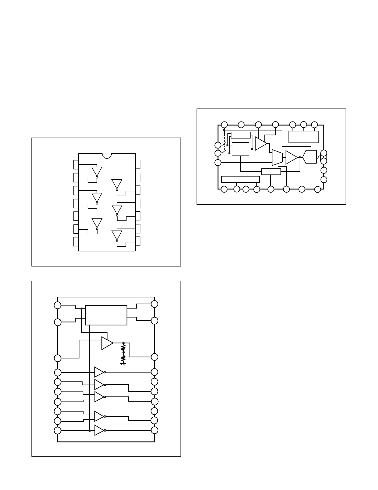
3. IC902 (H Driver) and IC904 (V Driver)
27
29
36
26
16
22
21
30
2319
11
12
17
PBLK
A/D
ACVDD
CMLEVEL
VRT
VTB
STBYCLPOB
ADCMODE
TIMING
GENERATOR
CLPDM PGACONT1
PGACONT2
SHP
SHD ADCCLK
PIN
DIN
ADCIN
DOUT
DRVDD
DVDD
ADVDD
2
37 20
18
47
48
43
3341
CLAMP
REFERENCE
CLAMP
CDS
PGA
MUX S/H
AD9802
10
An H driver (IC902) and V driver (IC904) are necessary in
order to generate the clocks (vertical transfer clock, horizontal transfer clock and electronic shutter clock) which driver
the CCD.
IC902 is an inverter IC which drives the horizontal CCDs (H1
and H2). In addition the XV1-XV4 signals which are output
from Pins (166), (167), (169) and (171) of IC102 are the vertical transfer clocks, and the XSG1 and XSG2 signals which
is output from Pins (168) and (170) of IC102 is superimposed
onto XV1 and XV3 at IC904 in order to generate a ternary
pulse. In addition, the XSUB signal which is output from Pin
(165) of IC102 is used as the sweep pulse for the electronic
shutter, and the RG signal which is output from Pin (159) of
IC102 is the reset gate clock.
14
CC
1A
1Y
2A
2Y
3A
1
2
3
4
5
V
13
6A
12
6Y
11
5A
10
5Y
4. IC905 (CDS, AGC Circuit and A/D converter)
The video signal which is output from the CCD is input to
Pins (26) and (27) of IC905. There are S/H blocks inside IC905
generated from the XSHP and XSHD pulses, and it is here
that CDS (correlated double sampling) is carried out.
After passing through the CDS circuit, the signal passes
through the AGC amplifier. It is A/C converted internally into
a 10-bit signal, and is then input to IC102 of the CA2 circuit
board. The gain of the AGC amplifier is controlled by the voltage at pin (29) which is output from IC102 of the CA2 circuit
board and smoothed by the PWM.
Fig. 1-4. IC905 Block Diagram
1
2
3
4
5
6
7
8
9
10
6
3Y
7
GND
Fig. 1-2. IC902 Block Diagram
CPP3
VH
Change Pump
+
‑
DCIN
XSHT
XV2
XV1
XSG1
XV3
XSG2
XV4
Fig. 1-3. IC904 Block Diagram
DC OUT
CPP1
CPP2
VSHT
9
8
VL
Vφ2
φ1
V
VM
Vφ3
Vφ4
4A
4Y
20
19
18
17
16
15
14
13
12
11
−3−
Page 4
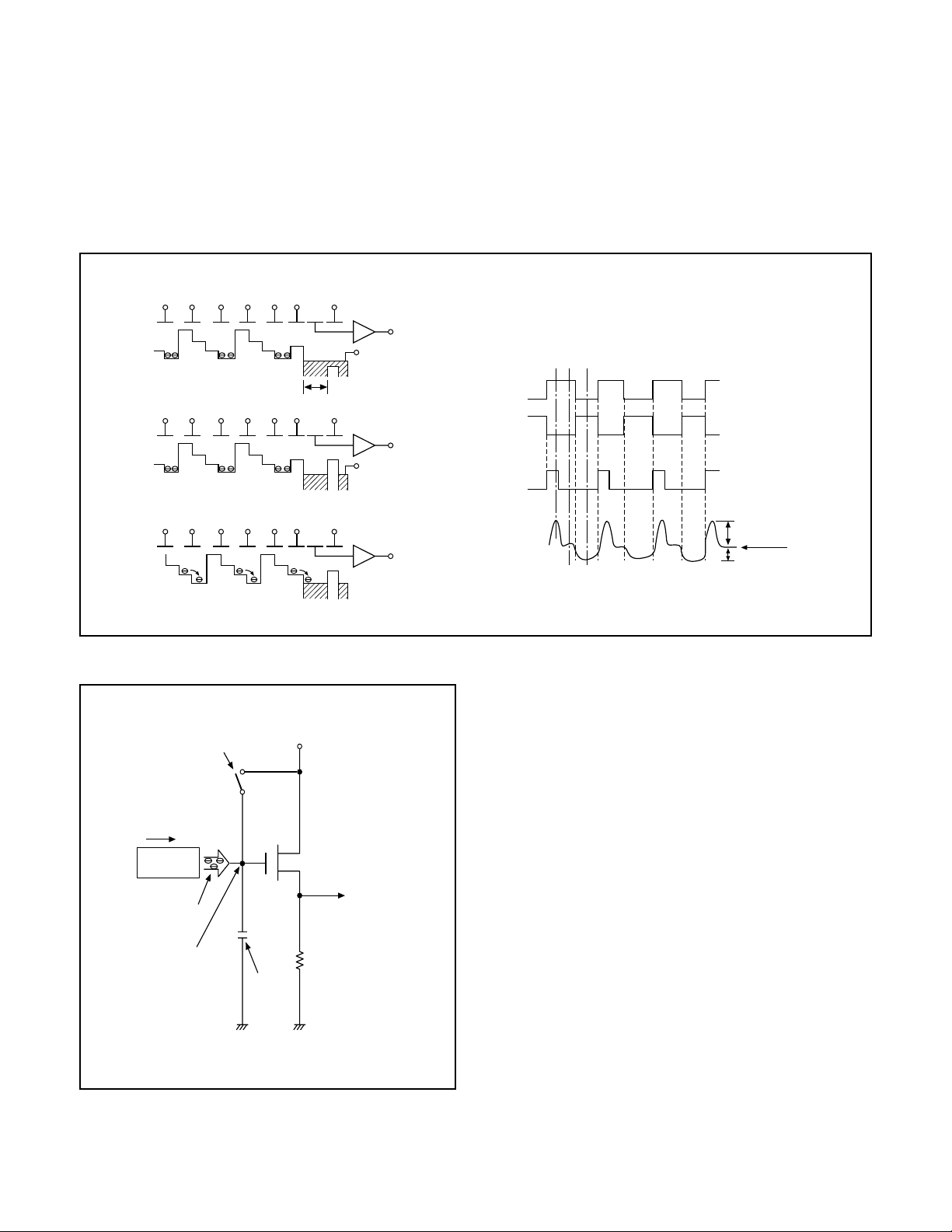
5. Transfer of Electric Charge by the Horizontal CCD
The transfer system for the horizontal CCD emplays a 2-phase drive method.
The electric charges sent to the final stage of the horizontal CCD are transferred to the floating diffusion, as shown in Fig. 1-5.
RG is turned on by the timing in (1), and the floating diffusion is charged to the potential of PD. The RG is turned off by the timing
in (2). In this condition, the floating diffusion is floated at high impedance. The H1 potential becomes shallow by the timing in (3),
and the electric charge now moves to the floating diffusion.
Here, the electric charges are converted into voltages at the rate of V = Q/C by the equivalent capacitance C of the floating
diffusion. RG is then turned on again by the timing in (1) when the H1 potential becomes deep.
Thus, the potential of the floating diffusion changes in proportion to the quantity of transferred electric charge, and becomes
CCD output after being received by the source follower. The equivalent circuit for the output circuit is shown in Fig. 1-6.
(1)
H1 H2 H1 H2 H1 HOG RG
CCD OUT
Floating diffusion
(2)
H1 H2 H1 H2 H1 HOG RG
PD
H1
H2
CCD OUT
PD
RG
(1) (2) (3)
3.5V
0V
3.5V
0V
13.5V
0V
(3)
H1 H2 H1 H2 H1 HOG RG
Reset gate pulse
Direction of transfer
H Register
Electric
charge
Floating diffusion gate is
floated at a high impedance.
CCD OUT
CCD OUT
Fig. 1-5. Horizontal Transfer of CCD Imager and Extraction of Signal Voltage
12V Pre-charge drain bias(PD)
Voltage output
C is charged
equivalently
RG pulse peak signal
RG pulse leak signal
Signal voltage
Black level
Fig. 1-6. Theory of Signal Extraction Operation
−4−
Page 5

1-2. CA2 CIRCUIT DESCRIPTION
1. Circuit Description
1-1. Scannning converter (Interlace converter)
This circuit uses the function of a 64-Mbit SDRAMs to convert the non-interlaced signal which is output from the CCD
into an interlaced signal for the video monitor.
1-2. Camera signal processor
This comprises circuits such as the digial clamp circuit, white
balance circuit, γcircuit, color signal generation circuit, matrix circuit and horizontal aperture circuit.
1. Digital clamp circuit
The optical black section of the CCD extracts 16-pixel averaged values from the subsequent data to make the black level
of the CCD output data uniform for each line. The 16-pixel
averaged value for each line is taken as the sum of the value
for the previous line multiplied by the coefficient k and the
value for the current line multiplied by the coefficient 1-k.
2. White balance circuit
This circuit controls the white balance by using the A WB judgement value computed by the CPU to control the gain for each
R, G and B pixel based on the CCD data which has been
read.
3. γ circuit
This circuit performs (gamma) correction in order to maintain
a linear relat ionship b etween the light i nput to the camer a
and the light output from the picture screen.
4. Color generation circuit
This circuit converts the CCD da ta int o RGB signal s.
5. Matrix circuit
This circuit generates the Y s ignals , R-Y signals and B-Y signals from the RGB signals.
1-7. 8-bit D/A circuit (Audio)
This circuit converts the audio signals (analog signals) from
the microphone to 8-bit digital signals.
1-8. 8-bit A/D circuit (Audio)
The audio signals which were converted to digial form by the
8-bit A/D circuit are temporarily to a sound buffer and then
recorded in the SSFDC card. During playback, the 8-bit D/A
circuit converts these signals into analog audio signals.
1-9. Sound buffer
Audio memory
1-10. LCD driver
The Y/C signals which are input to the LCD driver are converted to RGB signals, and the timing signal which is necessary for LCD monitor display and the RGB signals are then
supplied to the LCD monitor.
1-11. LCD monitor
This is the image display device which displays the image
signals supplied from the LCD driver.
1-12. UART
This circuit is used for transmitting serial data to a PC. The
interface is RS-232C-compatible.
1-13. SSFDC control
This reads data from the SSFDC card and stores it in SDRAM,
and writes out the image data stored in SDRAM. In addition,
error correction is carried out when the data is read.
1-14. MJPEG compression
Still and continuous frame data is converted to JPEG format,
and movie images are compressed and expanded in MJPEG
format.
6. Horizontal aperture circuit
This circuit is used generate the aperture signal.
1-3. SDRAM controller
This circuit outputs address, RAS, CAS and AS data for controlling the SDRAM. It also refr eshes the S DRA M.
1-4. PIO
The expansion parallel port can be used for functions such
as stroboscope control and LCD driver control.
1-5. SIO (Serial control)
This is the interface for the 8-bit mic roprocessor.
1-6. TG, SG block
This is the timing generation circuit which generates the clocks
(vertical transfer clock and electronic shutter clock) which drive
the CCD.
2. Outline of Operation
When the shutter opens, the reset signals, TEST0, TEST1
and the serial signals (“take a picture” commands) from the
8-bit microprocessor are input and record operation starts.
When the TG drives the CCD, picture data passes through
the A/D and is then input to the ASIC as 10-bit data. This data
then passes through the DCLP, AWB, shutter and γcircuit,
after which it is input to the SDRAM. The AWB, shutter, γ,
and AGC value are computed from this data, and two exposures are made to obtain the optimum picture. The data which
has already been stored in the SDRAM is read by the CPU
and color generation is carried out. Each pixel is interpolated
from the surrounding data as being either R, G or B primary
color data to produce R, G and B data. At this time, correction
of the lens distortion which is a characteristic of wide-angle
lenses is carried out. Aperture correction is carried out, and
in case of still picture the data is then compressed by the
JPEG method and in case of picture it is compressed by
MJPEG method and is written to SSFDC card. When the data
is to be output to an external device, it is read JPEG picture
data from the SSFCD card and output to PC via the UART.
−5−
Page 6

3. LCD Block
During EE, gamma conversion is carried out for the 10-bit
RGB data which is input from the A/D conversion block of the
CCD to the ASIC in order that the γrevised can be displayed
on the video. The YUV of 640 x 480 is then transferred to the
SVRAM.
The data which has accumulated in the SDRAM is after D/A
conversion is carried out by SDRAM control circuit inside the
ASIC , makes Y/C signal, the data is sent to the LCD panel
and displayed.
If the shutter button is pressed in this condition, the 10-bit
data which is output from the A/D conversion block of the
CCD is sent to the SDRAM (DMA transfer), and is displayed
on the LCD as a freeze-frame image.
During playback, the JPEG image data which has accumulated in the SSFDC card is converted to RGB signals. In the
same way as for EE, the data is then sent to the SDRAM,
after which D/A conversion is carried out inside the ASIC,
and then the data is sent to the LCD panel and displayed.
The LCD driver is converted Y/C signals to RGB signals from
ASIC, and these RGB signals and the control signal which is
output by the LCD driver are used to drive the LCD panel.
The RGB signals are 1H transposed so that no DC component is present in the LCD element, and the two horizontal
shift register clocks drive the horizontal shift registers inside
the LCD panel so that the 1H transposed RGB signals are
applied to the LCD panel.
Because the LCD closes more as the difference in potential
between the VCOM (common polar voltage: fixed at DC) and
the R, G and B signals becomes greater, the display becomes
darker; if the difference in potential is smaller, the element
opens and the LCD become brighter. In addition, the brightness and contrast settings for the LCD can be varied by means
of the serial data from the ASIC.
−6−
Page 7

1-3. PW1 POWER CIRCUIT DESCRIPTION
1. Outline
This is the main power circuit, and is comprised of the following blocks.
Switching controller (IC501)
Digital and analog system and LCD 5.0 V system power output (L5010, Q5002, D5013, C5061)
Digital 3.3 V system power supply (L5017, Q5009, D5007,
C5062)
Analog and LCD system power supply (Q5007, T5001)
Backlight power supply output (L5005, Q5008, D5014, C5005)
2. Switching Controller (IC501)
This is the basic circuit which is necessary for controlling the
power supply for a PWM-type switching regulator, and is provided with four built-in channels, only CH1 (digital 3.3 V), CH2
(5 V system), CH3 (analog and LCD system) and CH4 (backlight system) are used. Feedback from 3.3 V (D) (CH1) ,5.0 V
(D) (CH2), +15.0 V (A), +12.4 V (L) (CH3) and 5.8 V (L) (CH4)
power supply outputs are received, and the PWM duty is varied so that each one is maintained at the correct voltage setting level.
2-1. Short-circuit protection circuit
If output is short-circuited for the length of time determined
by the condenser which is connected to Pin (17) of IC501, all
output is turned off. The control signal (P ON, P(A) ON and
LCD ON) are recontrolled to restore output.
3. Digital 3.3 V Power Output
3.3 V (D) is output. Feedback for the 3.3 V (D) is provided to
the switching controller (Pins (1) of IC501) so that PWM control can be carried out.
4. 5 V System Power Output
5 V (D), 5.1 V (A) and 5 V (L) are output. Feedback for the 5
V (D) is provided to the switching controller (Pin (12) of IC501)
so that PWM control can be carried out.
5. Analog and LCD System Power Output
15.0 V (A), -7.5 V (A), 12.4 V (L) and 15 V (L) are output.
Feedback for the 15.0 V (A) with view mode and 12.4 V (L)
with play mode is provided to the switching controller (Pin
(25) of IC501) so that PWM control can be carried out.
6. Backlight Power Supply output
5.8 V (L) is output. Feedback is sent to pins (36) of the switching controller (IC501) for PWM control to be carried out.
−7−
Page 8

1-4. PW1 STROBE CIRCUIT DESCRIPTION
1. Charging Circuit
When UNREG power is supplied to the charge circuit and the
CHG signal becomes High (3.3 V), the charging circuit starts
operating and the main electorolytic capacitor is charged with
high-voltage direct current.
However, when the CHG signal is Low (0 V), the charging
circuit does not operate.
1-1. Power switch
When the CHG signal switches to Hi, Q5406 turns ON and
the charging circuit starts operating.
1-2. Power supply filter
L5401 and C5401 constitute the power supply filter. They
smooth out ripples in the current which accompany the switching of the oscillation transformer.
1-3. Oscillation circuit
This circuit generates an AC voltage (pulse) in order to increase the UNREG power supply voltage when drops in current occur. This circuit generates a drive pulse with a frequency
of approximately 50-100 kHz. Because self-excited light omission is used, the oscillation frequency changes according to
the drive conditions.
2. Light Emission Circuit
When RDY and TRIG signals are input from the ASIC expansion port, the stroboscope emits light.
2-1. Emission control circuit
When the RDY signal is input to the emission control circuit,
Q5409 switches on and preparation is made to let current
flow to the light emitting element. Moreover, when a STOP
signal is input, the stroboscope stops emitting light.
2-2. Trigger circuit
When a TRIG signal is input to the trigger circuit, D5405
switches on, a high-voltage pulse of several kilovolts is generated inside the trigger circuit, and this pulse is then applied
to the light emitting part.
2-3. Light emitting element
When the high-voltage pulse form the trigger circuit is applied to the light emitting part, currnet flows to the light emitting element and light is emitted.
※ Beware of electric shocks.
1-4. Oscillation transformer
The low-voltage alternating current which is generated by the
oscillation control circuit is converted to a high-voltage alternating current by the oscillation transformer.
1-5. Rectifier circuit
The high-voltage alternating current which is generated at
the secondary side of T5401 is rectified to produce a highvoltage direct current and is accumulated at electrolytic capacitor C5412 on the main circuit board.
1-6. Voltage monitoring circuit
This circuit is used to maintain the voltage accumulated at
C5412 at a constance level.
After the charging voltage is divided and converted to a lower
voltage by R5417 and R5419, it is output to the SY1 circuit
board as the monitoring voltage VMONIT. When this VMONIT
voltage reaches a specified level at the SY1 circuit board, the
CHG signal is switched to Low and charging is interrupted.
−8−
Page 9
1-5. SY1 CIRCUIT DESCRIPTION
1. Configuration and Functions
For the overall configuration of the SY1 circuit board, refer to the block diagram. The configuration of the SY1 circuit board
centers around a 8-bit microprocessor (IC301).
The 8-bit microprocessor handles the following functions.
1. Operation key input, 2. Mode LCD display, 3. Clock control, 4. Power ON/OFF, 5. Storobe charge control
Pin Signal
1
2
3~7
8
9
10
11
12
13
14~19
20
21
22
23~30
31
32~69
70
71
72
73
74
75
76
77
78
79
80
81
82
83
84
85
86
87
88~90
91~93
94
95
96
97
98
99
100
CHG VOL
NOT USED
SCAN IN 0~4
AVDD
AVREF
STBY (R) LED
STBY (G) LED
VSS
SELF LED (R)
NOT USED
AVREF ON
NOT USED
CHG ON
NOT USED
VSS
NOT USED
P (A) ON
P ON
DIN CONNECT
NOT USED
AV JACK
SCK
XOUT
VDD
XCIN
XCOUT
RESET
BAT OFF
RXD
S. REQ
NOT USED
SCAN OUT 0~2
NOT USED
LCD ON
ASIC TEST 0
ASIC RESET
ASIC TEST 1
AVSS
BATTERY
SI
SO
IC
XIN
I/O
I
I
I
O
O
-
O
-
O
-
O
-
-
-
O
O
I
I
I
O
O
-
O
I
I
O
I
I
I
I
-
O
-
O
O
O
O
-
I
Table 4-1. 8-bit Microprocessor Port Specification
Strobe charge voltage input (analog input)
Key matrix input
A/D converter analog power terminal
A/D converter standard voltage input terminal
Standby LED (red) ON/OFF signal L : LED light
Standby LED (green) ON/OFF signal L : LED light
GND
Self-timer LED (red) ON/OFF signal L : LED light
A/D standard power ON/OFF signal L : ON
Flash charge ON/OFF signal H : ON
GND
DC/DC converter (analog) ON/OFF signal H : ON
DC/DC converter (digital) ON/OFF signal H : ON
DIN jack connect detection signal L : Connection
AV output cable connection detection signal L : Connection
Serial communication data input (←ASIC)
Serial communication data output (→ASIC)
Serial communication clock output (→ASIC)
Connect to Vss
Main clock oscillation terminal (4 MHz)
Main clock oscillation terminal
Power supply terminal
Sub clock oscillation terminal (32.768 kHz)
Sub clock oscillation terminal
Reset input
Battery OFF detection signal L : OFF
RS-232C RXD input terminal
Serial communication request signal L : Request
Key matrix output
-
LCD monitor power ON/OFF signal H : ON
ASIC reset control signal
ASIC reset signal L : Reset output
ASIC reset control signal
A/D converter GND power terminal
Battery voltage input (analog input)
−9−
Outline
Page 10

2. Internal Communication Bus
The SY1 circuit board carries out overall control of camera operation by detecting the input from the keyboard and the condition
of the camera circuits. The 8-bit microprocessor reads the signals from each sensor element as input data and outputs this data
to the camera circuits (ASIC) or to the LCD display device as operation mode setting data. Fig. 4-1 shows the internal communication between the 8-bit microprocessor and ASIC.
S. REQ
8-bit
microprocessor
Fig. 4-1 Internal Bus Communication System
ASIC SO
ASIC SI
ASIC SCK
RESET
3. Key Operaiton
For details of the key operation, refer to the instruction manual.
SCAN
SCAN
OUT
IN
0
1
23
0
1
2
SHUTTER 1st
BARRIER
SHUTTER 2nd
CARD LID
Table 4-2. Key Operation
CAMERA
MODE
PLAY
SET
ASIC
32 bit
CPU
4
MACRO
-
TEST
−10−
Page 11

4. Power Supply Control
The 8-bit microprocessor controls the power supply for the overall system.
The following is a description of how the power supply is turned on and off. When the battery is attached, a regulated 3.3 V
voltage is normally input to the 8-bit microprocessor (IC301) by IC303, so that clock counting and key scanning is carried out
even when the power switch is turned off, so that the camera can start up again. When the battery is removed, the 8-bit microprocessor operates in sleep mode using the backup capacitor. At this time, the 8-bit microprocessor only carries out clock
counting, and waits in standby for the battery to be attached again. When a switch is operated, the 8-bit microprocessor supplies
power to the system as required.
The 8-bit microprocessor first sets both the P (A) ON signal at pin (70) and the P ON signal at pin (71) to low, and then turns on
the DC/DC converter. After this, High signals are output from pin (97) so that the ASIC is set to the active condition. If the LCD
monitor is on, the LCD ON signal at pin (95) set to Low, and the DC/DC converter for the LCD monitor is turned on.
Lens
cover
open
Power voltage
Lens cover close
Power switch ON-
Auto power down
Shutter switch ON
Resolution, Flash,
Self timer switch ON
LCD finder
Playback
Power voltage
ASIC,
memory
3.3 V 3.3 V
OFF OFF
OFF OFF
ON ON
OFF OFF
ON ON
ON ON
Table 4-3. Camera Mode (Battery Operation)
ASIC,
memory
3.3 V 3.3 V
RS232C
driver
RS232C
Driver
CCD
5 V (A), -7.5 V ,
+15 V etc.
OFF
OFF
ON→ OFF
OFF
ON
OFF
CCD
5 V (A), -7.5 V ,
+12 V etc.
8bit
CPU
3.2 V
(ALWAYS)
32KHz OFF OFF
4MHz ON OFF
4MHz ON OFF
4MHz ON OFF
4MHz ON ON
4MHz ON ON
8bit
CPU
3.2 V
(ALWAYS)
MODE
LCD
3.2 V
(ALWAYS)
MODE
LCD
3.2 V
(ALWAYS)
MONITOR
5V (L), 15 V,
+12V etc.
MONITOR
+12V etc.
LCD
LCD
5 V (L)
Lens cover close
Power switch ON-
Auto power down
Take a picture
Lens
cover
open
Note) P. SAVE = Power save mode, 4 MHz = Main clock operation, 32 kHz = Sub clock operation
Erase image
Download image
Continuous image
Message from host
Table 4-4. Host Mode (Battery Operation)
OFF OFF
OFF OFF
ON ON
ON ON
ON ON
ON ON
ON ON
−11−
OFF
OFF
ON→ OFF
OFF
OFF
ON
ON
32 KHz OFF OFF
4 MHz ON OFF
4 MHz ON OFF
4 MHz ON OFF
4 MHz ON OFF
4 MHz ON OFF
4 MHz ON OFF
Page 12

2. DISASSEMBL Y
2-1. REMOV AL OF CABINET ASSEMBLY (FRONT) AND CABINET ASSEMBLY (BACK)
13. Holder battery
2. Front cabinet
7. Cabinet top
10. Holder
SSFDC
6. Screw 1.7 x 3
3. Back cabinet
12. Five screws
1.7 x 3
1. Four screws
1.7 x 4
11. Holder terminal
5. Cover jack
8. Screw 1.7 x 3
9. Two screws
1.7 x 4
1. Two screws 1.7 x 4
4. Cover battery
2-2. REMOV AL OF SY1 BOARD, TB2 BOARD AND TB1 BOARD
1. Two screws 1.7 x 3
4. Connector
3. Three connectors
7. TB2 board
2. FPC
5. SY1 board
9. Unit control panel
8. Screw 1.7 x 3
6. Screw 1.7 x 3
10. Screw 1.7 x 3
11. TB1 board
−12−
Page 13

2-3. REMOV AL OF LENS VF AND PW1 BOARD
1. Two screws 1.7 x 3
2. Lens VF
4. Connector
3. Two screws
1.7 x 3
5. Connector
8. Reflector
6. Three
screws
1.7 x 3
7. Holder chassis PW1
9. PW1 board
−13−
Page 14

2-4. REMOV AL OF LCD, CA2 BOARD AND CA1 BOARD
9. CA2 board
7. Two
screws
1.7 x 3
6. Two
connectors
8. Holder
chassis
CA2
4. Connector
5. Screw 1.7 x 3
3. Four screws
1.7 x 3
11. Holder
chassis
CA1
12. Two screws
1.7 x 6
13. Screw
1.7 x 4
2. LCD
1. FPC
2-5. BOARD LOCA TION
TB2 board
CA2 board
10. Three screws
1.7 x 3
SY1 board
14. CA2 board
TB1 board
PW1 board
CA1 board
−14−
Page 15

3. ELECTRICAL ADJUSTMENT
3-1. Table for Servicing Tools
Ref. No.
J-1
J-2
J-3
J-4
Note: J-1 color viewer is 100 - 110 VAC only.
Color viewer 5,100 K
Siemens star chart
Calibration software
Extension cord
J-2 Siemens star chart is the same as before models.
J-1 J-2
Name
Part code
VJ8-0007
VJ8-0166
VJ8-0151
3-4. Setup
1. System requirements
Windows 95 or 98
IBM R -compatible PC with 486 or higher processor
CD-ROM drive
3.5-inch high-density diskette drive
Serial port with standard RS-232C interface
8 MB RAM
Hard disk drive with at least 15 MB available
VGA or SVGA monitor with at least 256-color display
2. Installing calibration software
1. Insert the calibration software installation diskette into your
diskette drive.
2. Open the explorer.
3. Copy the DSC Cal folder on the floppy disk in the FD drive
to a folder on the hard disk.
3. Color Viewer
Turn on the switch and wait for 30 minutes for aging to take
place before using Color Pure.
J-3
J-4
3-2. Equipment
1. Oscilloscope
2. Digital voltmeter
3. AC adaptor
4. IBM R -compatible PC
5. DC regulated power supply
3-3. Adjustment Items and Order
1. IC501 Frequency Adjustment
2. 5.0 V (D) Voltage Adjustment
3. 3.3 V (D) Voltage Adjustment
4. 12.4 V (L) Voltage Adjustment 1
5. 12.4 V (L) Voltage Adjustment 2
6. 5.8 V (L) Voltage Adjustment
7. CCD Defect Defect Adjustment
8. AWB Adjustment
9. Flange-back Adjustment
10. LCD Panel Adjustment
10-1. LCD H AFC Adjustment
10-2. LCD RGB Offset Adjustment
10-3. LCD Gain Adjustment
10-4. LCD Blue Brightness Adjustment
10-5. LCD Red Brightness Adjustment
4.Computer screen during adjustment
Calibration
AWB
Focus
UV Matrix
Firmware Version:
Upload
Firmware
Image
Initialize
LCD Type
LCD
R Bright
RGB Offset
Tint
H AFC Test
B Bright
Gain
Phase
VCOMDC
VCOMPP
−15−
Page 16

3-5. Connecting the camera to the computer
1. Turn off both camera and computer.
2. Locate the port cover on the side of the camera. Press on the arrows and slide the cover down to open it.
3. Line up the arrow on the cable connector with the notch on the camera's serial port. Insert the connector.
4. Locate a serial port on the back of your computer. You may have two serial ports labeled COM1 and COM2, or the ports may
be labeled with icons. If you have two serial ports available, use port 1 to connect your camera.
5. Line up the serial connector on the cable with one of the serial ports on your computer, and insert the connector.
6. Turn on the camera and your computer system.
To COM1 or COM2 serial port
Serial cable
AC adaptor
−16−
Page 17

3-6. Adjust Specifications
[PW1 board (Side A/B)]
VR501
VR505
CL515
CL554
VR504
VR503
VR502
CL524
CL519
CL530
CL536
VR506
3. 3.3 V (D) Voltage Adjustment
Measuring Point
Measuring Equipment
ADJ. Location
ADJ. Value
Adjustment method:
1.Adjust with VR502 to 3.30 ± 0.03 V.
CL533 or CL553 or CL519
Digital voltmeter
VR502
3.30 ±0.03 V
4. 12.4 V (L) Voltage Adjustment 1
Measuring Point
Measuring Equipment
ADJ. Location
ADJ. Value
CL524 or CL554
Digital voltmeter
VR505
12.40 ±0.05 V
CL512
CL553
CL533
Note:
1. Voltage adjustment is necessary to repair in the PW1 board
and replace the parts.
2. Power voltage set about +3.0 V.
Preparation:
1. Connect CN103 on the CA2 board and CN502 on the PW1
board with extension cord.
2. Open the barrier switch.
3. Set the view mode, and turn on the LCD.
4. Carry out initialization and display the through image on the
LCD screen.
1. IC501 Oscillation Frequency Adjustment
Adjustment method:
1. Set the play mode.
2. Adjust with VR505 to 12.40 ± 0.05 V.
5. 12.4 V (L) Voltage Adjustment 2
Measuring Point
Measuring Equipment
ADJ. Location
ADJ. Value
Adjustment method:
1. Set the view mode, and turn on the LCD.
2. Adjust with VR504 to 12.40 ± 0.05 V.
CL524 or CL554
Digital voltmeter
VR504
12.40 ±0.05 V
6. 5.8 V (L) Voltage Adjustment
Measuring Point
Measuring Equipment
ADJ. Location
ADJ. Value
Adjustment method:
1. Adjust with VR506 to 5.80 ± 0.05 V.
CL530 or CL536
Digital voltmeter
VR506
5.80 ±0.05 V
Measuring Point
Measuring Equipment
ADJ. Location
ADJ. Value
CL512
Frequency counter
VR501
200 ±1 kHz
Adjustment method:
1. Adjust with VR501 to 200 ±1 kHz.
2. 5.0 V (D) Voltage Adjustment
Measuring Point
Measuring Equipment
ADJ. Location
ADJ. Value
Adjustment method:
1. Adjust with VR503 to 5.10 ±0.05 V.
CL515
Digital voltmeter
VR503
5.10 ±0.05 V
7. CCD Defect Detect Adjustment
Adjustment method:
1. Set the camera mode, and turn on the power switch to open
the lens cover.
2. Double-click on the DscCalV123b.
3. Select CCD Defect on the LCD “Test”, and click the “Yes”.
4. After the adjustment is completed, OK will display.
5. Close the lens cover.
−17−
Page 18

8. AWB Adjustment
Serial cable
Camera
Preparation:
POWER switch: ON
Adjusting method:
1. Set the all white pattern so that it becomes a full picture.
(Do not enter any light.)
2. Double-click on the DscCalV123b.
3. Click the AWB, and click the Yes.
4. AWB adjustment value will appear on the screen.
5. Click the OK.
0 - 18 cm
All white pattern
Color viewer(5,100K)
Preparation:
POWER switch: ON
Adjusting location:
Flange-back adjustment screw (Fig. 1)
Adjust the adjustment screw by turning it through the hole provided in the CA1 board. If this adjustment screw is turned
counter-clockwise, the focal length of the lens will decrease,
and if it is turned clockwise, the focal length will increase.
Adjustment method:
1. Display the image taken by the camera on the screen of a
computer.
2. Set the focus switch at the normal position.
3. Project two Siemens star charts at a distance of 1.0 meters
and 0.3 meters infront of the lens.
4. Turn the adjustment screw until the Siemens star which is
1.0 meters away is exactly in focus. Check that the Siemens
star which is 0.3 meters from the front of the lens is out of
focus at this time.
5. Project the Siemens star chart at a distance of 0.3 meters
in front of lens. Check that it is out of focus at normal mode,
and it is in focus at macro mode.
6. This adjustment location is integrated with the iris mechanism. After adjusting, make sure that no load has been
placed on the iris mechanism and harness.
10. LCD Panel Adjustment
[CA1 board (Side B)]
9. Frange-back Adjustment
Lens
Fig. 1
Screw driver
Adjustment screw
Focus switch
Macro position
Normal position
CL426
CL424
CL425
10-1. LCD H AFC Adjustment
Preparation:
POWER switch: ON
Adjusting method:
1. Double-click on the DscCalV123b .
2. Select 0 on the LCD “H AFC”.
3. While watching the LCD monitor, adjust “H AFC” so that the
edge of the LCD adjustment frame are the same distance
from the left and right edge of the LCD screen. (A = B)
Fig. 2
−18−
Page 19

LCD screen
LCD
A
FPC
adjustment
B
frame
VG
10-2. LCD RGB Offset Adjustment
Adjusting method:
1. Adjust LCD “RGB offset” so that the amplitude of the CL424
waveform is 7.5 Vp-p ±0.3 V.
7.5 Vp-p
±0.3 V
CL424 waveform
10-3. LCD Gain Adjustment
Adjusting method:
1. Adjust LCD “Gain” so that the amplitude of the CL424 waveform is 4.0 Vp-p ±0.15 V.
Note:
10-2. LCD RGB Offset adjustment should always be carried
out first.
CL424 waveform
VG± 0.2 V
CL426 waveform
10-5. LCD Red Brightness Adjustment
Adjusting method:
1. Adjust LCD “R Bright” so that the amplitude of the CL425
waveform is ±0.2 V with respect to the CL424 (VG) waveform.
Note:
10-2. LCD RGB Offset adjustment and 10-3. LCD Gain adjustment should always be carried out first.
4.0 Vp-p
±0.15 V
CL424 waveform
10-4. LCD Blue Brightness Adjustment
Adjusting method:
1. Adjust LCD “B Bright” so that the amplitude of the CL426
waveform is ±0.2 V with respect to the CL424 (VG) waveform.
Note:
10-2. LCD RGB Offset adjustment and 10-3. LCD Gain adjustment should always be carried out first.
VG
CL424 waveform
VG± 0.2 V
CL425 waveform
−19−
Page 20

4. TROUBLESHOOTING GUIDE
POWER LOSS INOPERTIVE
BARRIER SW
OPEN
IC301-4, 93
LOW
IC302-7 (UP UNREG)
HIGH
IC301-81
(VDD)
HIGH
IC301-84
(RESET)
HIGH
IC301-85
(BAT OFF)
HIGH
IC301-80
OSCILLATION
YES
IC301-82
OSCILLATION
YES
CLOSE
BARRIER SW ON
HIGH
CN302, D3069, R3021
LOW
CHECK IC132, PW1
LOW
LOW
CHECK IC302, R3051
LOW
NO
NO
R3004, C3001, C3002
CHECK S6002,
CHECK IC302
CHECK R3052
CHECK X3001
CHECK X3002,
NORMAL
TAKING INOPERATIVE
PUSH SHUTTER
BUTTON
IC301-4, 5
(SCAN IN 0, 1)
PULSE INPUT
YES
IC301-70, 71
(P ON, P(A) ON)
HIGH
IC301-96, 97, 98
HIGH
YES
SERIAL
COMMUNICATION
IC301-75~77, 87
OK
CHECK IC101
NO
LOW
NO
CHECK IC301, IC101
NG
R3001, R3003, IC101
CHECK
S3029, D3064,
R3021, R3022
CHECK IC301
CHECK IC301,
CHECK IC301
NO PICTURE
CLK (114MHz)
OSCILLATION
CHECK L1105
YES
SD CLK (57 MHz)
OSCILLATION
IC106-35
YES
IC101-111, 114
(IC301-75, 76)
OK
CHECK ASIC AND
MEMORY PIN
MAIN CLOCK FOR SYSTEM OPERATION
YES
NO OPERATION IF ABSENT
CHECK IC111, L1101, L1105 and X1101
MAIN CLOCK FOR SDRAM (IC106)
NG
NO OPERATION IF ABSENT FROM IC121
CHECK IC101, IC106 and C1061
INCORRECT HANDSHAKING BETWEEN 8-BIT
NG
CPU AND RS-232C
CHECK EACH INTERFACE
−20−
Page 21

5 . PARTS LIST
CABINET & CHASSIS PARTS 1
1 636 056 2479 ASSY,COVER LENS-SR662/E
2 636 055 5600 COVER FRONT-SR662/J
3 636 055 5785 DEC WINDOW VF-SR662/J
4 636 055 5792 DEC STRAP-SR662/J
5 636 055 9066 ASSY,CABI FRONT-SR662/J
6 636 055 5846 HOLDER COVER LENS-SR662/J
7 636 055 6041 SPRING LENS-SR662/J
8 636 055 5921 KNOB MACRO-SR662/J
9 636 055 5976 SLIDE KNOB MACRO-SR662/J
10 636 055 6010 SPRING P SSFDC-SR662/J
11 636 055 9103 COMPL,COVER BATTERY-662/J
12 636 055 5761 COVER SSFDC-SR662/J
13 636 056 6460 SHIELD TAPE SSFDC-SR662/J
14 636 055 5907 HOLDER SSFDC-SR662/J
15 636 055 5747 COVER JACK-SR662/J
LOCATION PARTS NO. DESCRIPTIONLOCATION PARTS NO. DESCRIPTION
16 636 055 5853 HOLDER TERMINAL-SR662/J
17 636 056 0956 DEC MONITOR-SR662/E
18 636 055 9080 ASSY,CABINET BACK-SR662/J
19 636 055 5938 KNOB POWER-SR662/J
20 636 057 0214 SPRING COMP RELEASE-662/J
21 636 055 9042 ASSY,BUTTON SHUTTER-662/J
22 636 056 0932 CABINET TOP-SR662/E
23 636 055 5990 SLIDE KNOB POWER-SR662/J
24 636 055 6058 TERMINAL BATTERY A-SR662J
25 636 055 6065 TERMINAL BATTERY B-SR662J
26 636 055 5891 HOLDER BATTERY-SR662/J
27 636 055 4658 LABEL CAUTION BATT-SX112J
101 411 017 7508 SCR PAN PCS 1.4X2
102 411 178 8802 SCR S-TPG PAN PCS 1.7X2.0
103 411 175 5705 SCR PAN PCS 1.7X3
104 411 178 9403 SCR S-TPG PAN PCS 1.7X4.0
105 411 177 8407 SCR S-TPG PAN PCS 1.7X3
N.S.P.: Not available as service parts.
17
22
23
21
20
19
103
18
104
104
105
26
27
24
25
105
105
104
104
4
105
5
6
1
104
SR622/J PartsList 1
104
101
3
7
8
102
10
9
16
15
104
14
2
103
11
13
12
21
Page 22

CABINET & CHASSIS PARTS 2
1 645 029 2170 LENS(ASSY)
2 645 032 5854 OPTICAL FILTER
3 636 052 2183 SPACER
4 636 052 9199 ASSY,UNIT,CCD
5 636 052 2190 SPACER,INSULATOR
6 636 057 3093 SPACER CHASSIS PW1-SR662J
7 636 055 4252 COMPL PWB,CA-1,VPC-X360 ONLY
7 636 056 2431 COMPL PWB,CA-1,EXCEPT VPC-X360
8 636 055 5839 HOLDER CHASSIS CA1-662/J
9 645 039 9732 UNIT,CONTROL PANEL
10 636 056 1298 SPACER UNIT C.P-SR662/J
11 645 032 2167 LCD
12 636 055 9189 SPACER MONITOR BTM-662/J
13 636 055 5983 SLIDE MACRO-SR662/J
14 636 055 4306 COMPL PWB,TB-1
15 636 055 5815 HOLDER CHASSIS CA2-662/J
24
106
23
103
103
25
26
103
LOCATION PARTS NO. DESCRIPTIONLOCATION PARTS NO. DESCRIPTION
16 636 055 4276 COMPL PWB,CA-2,EXCEPT VPC-X360
16 636 056 6705 COMPL PWB,CA-2,VPC-X360 ONLY
17 636 055 4290 COMPL PWB,PW-1
18 636 055 5822 HOLDER CHASSIS PW1-662/J
19 636 055 4313 COMPL PWB,TB-2
20 636 055 8892 COMPL,REFLECTOR
21 636 055 4283 COMPL PWB,SY-1
22 636 055 5877 HOLDER VF-SR662/J
23 645 023 4248 ASSY,LENS,VF
24 636 055 5952 REFLECTOR VF-SR662/J
25 645 030 0639 MICROPHONE
26 636 056 2615 ADHESIVE TAPE VF-SR661/J
103 411 175 5705 SCR PAN PCS 1.7X3
106 411 170 8602 SCR S-TPG PAN 2X5
107 411 169 9603 SCR S-TPG PAN PCS 1.7X6E
108 411 020 0701 SCR PAN PCS 1.7X4
N.S.P.: Not available as service parts.
103
19
21
103
106
15
16
22
14
103
20
6
6
103
103
103
103
13
103
17
11
12
18
103
108
10
103
107
5
4
3
1
2
103
103
7
22
8
9
SR622/J PartsList 2
103
Page 23

ELECTRICAL PARTS
Note:
1. Materials of Capacitors and Resistors are abbreviated as follows ;
Resistors Capacitors
MT-FILM Metallized Film Resistor MT-POLYEST Metallized Polyester Capacitor
MT-GLAZE Metallized Glaze Resistor MT-COMPO Metallized Composite Capacitor
OXIDE-MT Oxide Metallized Film Resistor TA-SOLD Tantalum Solid Capacitor
2. Tolerance of Capacitor (10pF over) and Resistor are noted with follow symboles.
F ............1% G ............2% J ............5% K ............10%
M ..........20% N ..........30% Z ..........+80% ~ -20%
3. Capacitors
µ
F P : pF
U :
4. Inductors
µ
H MH : mH
UH :
5. N.S.P. : Not available as service parts.
LOCATION PARTS NO. DESCRIPTION LOCATION PARTS NO. DESCRIPTION
COMPL PWB,CA-1
636 055 4252 VPC-X360 ONLY
636 056 2431 EXCEPT VPC-X360
Q1701 405 102 5609 TR 2SD1819A-R
OR 405 092 4101 TR 2SC4081-R
Q1702 405 115 6907 TR DTC114EE
Q1707 405 102 5500 TR 2SB1218A-R
OR 405 092 4200 TR 2SA1576-R
Q2001 405 102 5609 TR 2SD1819A-R
OR 405 092 4101 TR 2SC4081-R
Q2002 405 131 3607 TR DTA144EUA
Q2003 405 102 5609 TR 2SD1819A-R
OR 405 092 4101 TR 2SC4081-R
Q9001 405 079 6203 TR 2SC4399-4
OR 405 079 6302 TR 2SC4399-5
Q9002 405 133 8907 TR DTC114EUA
Q9007 405 129 2308 TR UMZ1N
OR 405 106 4806 TR XP4601
Q9010 405 102 5609 TR 2SD1819A-R
OR 405 092 4101 TR 2SC4081-R
IC171 409 452 4206 IC LV4127W
IC174 409 423 6802 IC TK11245BM
IC175 409 400 9109 IC TC7SET08FU
IC201 409 432 2505 IC LMV321M7X
IC202 409 432 2604 IC LMV821M7X
IC902 409 392 9101 IC 74VHC04MTC
IC904 409 366 9700 IC CXD1267AN
IC905 409 418 9702 IC AD9802JSTRL
IC909 409 407 0505 IC TK11331BM
D1701 407 166 0606 DIODE MA365
D9011 407 187 8407 ZENER DIODE UDZ16B
D9019 407 149 0807 DIODE 1SS355
D9020 407 198 9905 DIODE MA727
D9021 407 198 9905 DIODE MA727
D9022 407 198 9905 DIODE MA727
X1701 645 025 6004 OSC,CRYSTAL 3.579545MHZ,VPC-X360 ONLY
X1701 645 030 0431 OSC,CRYSTAL 4.433619MHZ,
L1701 645 021 1607 INDUCTOR,10U J
L1702 645 021 1607 INDUCTOR,10U J
L1703 645 020 1868 INDUCTOR,750 OHM
L1704 645 020 2070 INDUCTOR,750 OHM
L1705 645 020 1875 INDUCTOR,1500 OHM
L1706 645 020 1868 INDUCTOR,750 OHM
L1707 645 014 8064 INDUCTOR,120 OHM
L1708 645 020 2070 INDUCTOR,750 OHM
L1709 645 020 2070 INDUCTOR,750 OHM
L9001 645 001 4512 INDUCTOR,10U K
L9010 645 020 1875 INDUCTOR,1500 OHM
L9010 645 020 1882 INDUCTOR,1800 OHM
C1700 403 312 6805 CERAMIC 0.1U Z 16V
(SEMICONDUCTORS)
(INTEGRATED CIRCUITS)
(DIODES)
(CRYSTAL DEVICES)
EXCEPT VPC-X360
(INDUCTORS)
(CAPACITORS)
AL-SOLID Aluminum Solid Capacitor
NP-ELECT Non-Polarized Electrolytic Capacitor
OS-SOLID Aluminum Solid Capacitors with Organic
Semiconductive Electrolytic Capacitor
DL-ELECT Double Layered Electrolytic Capacitor
C1702 403 332 9503 CERAMIC 1U M 6.3V
C1703 403 311 4505 CERAMIC 1000P K 50V
C1705 403 312 6003 CERAMIC 39P J 50V
C1706 403 319 3005 CERAMIC 220P J 25V
C1707 403 311 3409 CERAMIC 0.01U K 16V
C1708 403 207 0307 CERAMIC 1U Z 16V
C1709 403 157 7302 CERAMIC 6800P K 50V
C1710 403 332 9503 CERAMIC 1U M 6.3V
C1711 403 283 6309 CERAMIC 1U Z 10V
C1712 403 332 9503 CERAMIC 1U M 6.3V
C1714 403 311 3409 CERAMIC 0.01U K 16V
C1715 403 311 3409 CERAMIC 0.01U K 16V
C1717 403 322 3504 CERAMIC 22U Z 10V
C1718 403 338 0405 CERAMIC 0.47U K 25V
C1719 403 338 0405 CERAMIC 0.47U K 25V
C1720 403 338 0405 CERAMIC 0.47U K 25V
C1721 403 338 0405 CERAMIC 0.47U K 25V
C1722 403 283 6309 CERAMIC 1U Z 10V
C1723 403 332 9503 CERAMIC 1U M 6.3V
C1724 403 309 8607 CERAMIC 18P J 50V,EXCEPT VPC-X360
C1724 403 311 4505 CERAMIC 1000P K 50V,VPC-X360 ONLY
C1726 403 207 0307 CERAMIC 1U Z 16V
C1727 403 332 9503 CERAMIC 1U M 6.3V
C1729 403 311 3409 CERAMIC 0.01U K 16V
C1730 403 312 6805 CERAMIC 0.1U Z 16V
C1731 403 347 9406 CERAMIC 0.22U Z 10V
C1739 403 327 0300 CERAMIC 10U Z 25V
C1741 403 325 4409 CERAMIC 0.068U Z 16V
C1742 403 347 9406 CERAMIC 0.22U Z 10V
C1775 403 207 0307 CERAMIC 1U Z 16V
C1776 403 332 9503 CERAMIC 1U M 6.3V
C1777 403 334 3806 CERAMIC 10U K 6.3V
C1778 403 332 8209 CERAMIC 10U M 16V
C1779 403 332 9503 CERAMIC 1U M 6.3V
C2010 403 323 6306 CERAMIC 0.1U K 16V
C2011 403 272 5603 CERAMIC 0.033U K 16V
C2012 403 311 7704 CERAMIC 4700P K 25V
C2014 403 332 9503 CERAMIC 1U M 6.3V
C2015 403 332 9503 CERAMIC 1U M 6.3V
C2016 403 332 9503 CERAMIC 1U M 6.3V
C2017 403 155 2101 CERAMIC 1500P K 50V
C2018 403 332 9503 CERAMIC 1U M 6.3V
C2019 403 334 3806 CERAMIC 10U K 6.3V
C9003 403 315 6406 CERAMIC 180P J 25V
C9004 403 320 5203 CERAMIC 0.33U K 16V
C9005 403 207 0307 CERAMIC 1U Z 16V
C9006 403 311 3409 CERAMIC 0.01U K 16V
C9007 403 312 6805 CERAMIC 0.1U Z 16V
C9008 403 155 1807 CERAMIC 0.01U K 25V
C9010 403 320 5500 CERAMIC 1U Z 25V
C9012 403 320 5500 CERAMIC 1U Z 25V
C9013 403 311 3409 CERAMIC 0.01U K 16V
C9014 403 311 7605 CERAMIC 2200P K 50V
C9016 403 068 0409 CERAMIC 0.1U Z 25V
C9018 403 311 3409 CERAMIC 0.01U K 16V
C9019 403 320 5500 CERAMIC 1U Z 25V
C9020 403 311 5809 CERAMIC 47P J 50V
C9021 403 164 0204 CERAMIC 0.1U Z 25V
23
Page 24

LOCATION PARTS NO. DESCRIPTION LOCATION PARTS NO. DESCRIPTION
C9022 403 312 6805 CERAMIC 0.1U Z 16V
C9023 403 320 5302 CERAMIC 0.15U K 25V
C9025 403 312 6805 CERAMIC 0.1U Z 16V
C9026 403 312 6805 CERAMIC 0.1U Z 16V
C9029 403 312 6805 CERAMIC 0.1U Z 16V
C9030 403 296 8000 TA-SOLID 22U M 10V
C9031 403 311 3409 CERAMIC 0.01U K 16V
C9032 403 312 6805 CERAMIC 0.1U Z 16V
C9033 403 312 6805 CERAMIC 0.1U Z 16V
C9034 403 312 6805 CERAMIC 0.1U Z 16V
C9035 403 325 7608 CERAMIC 1U K 16V
C9036 403 311 3409 CERAMIC 0.01U K 16V
C9037 403 283 6309 CERAMIC 1U Z 10V
C9038 403 283 6309 CERAMIC 1U Z 10V
C9039 403 311 3409 CERAMIC 0.01U K 16V
C9040 403 311 3409 CERAMIC 0.01U K 16V
C9041 403 312 6805 CERAMIC 0.1U Z 16V
C9042 403 283 6309 CERAMIC 1U Z 10V
C9043 403 283 6309 CERAMIC 1U Z 10V
C9044 403 311 3409 CERAMIC 0.01U K 16V
C9046 403 312 6805 CERAMIC 0.1U Z 16V
C9047 403 312 6805 CERAMIC 0.1U Z 16V
C9048 403 296 1308 TA-SOLID 10U M 20V
C9051 403 325 7608 CERAMIC 1U K 16V
C9052 403 320 5203 CERAMIC 0.33U K 16V
C9059 403 315 6406 CERAMIC 180P J 25V
C9060 403 315 6406 CERAMIC 180P J 25V
C9061 403 315 6406 CERAMIC 180P J 25V
C9062 403 315 6406 CERAMIC 180P J 25V
C9064 403 315 6406 CERAMIC 180P J 25V
C9065 403 315 6406 CERAMIC 180P J 25V
C9066 403 315 6406 CERAMIC 180P J 25V
C9067 403 296 1308 TA-SOLID 10U M 20V
C9080 403 315 6406 CERAMIC 180P J 25V
C9081 403 190 4306 CERMAIC 0.1U K 25V
(RESISTORS)
R1701 401 224 9204 MT-GLAZE 15K JA 1/16W
R1702 401 258 6804 MT-GLAZE 15K DC 1/16W
R1703 401 262 1406 MT-GLAZE 4.3K DC 1/16W
R1704 401 224 9204 MT-GLAZE 15K JA 1/16W
R1705 401 224 9006 MT-GLAZE 10K JA 1/16W
R1706 401 262 0904 MT-GLAZE 27K DC 1/16W
R1707 401 262 0706 MT-GLAZE 39K DC 1/16W
R1709 401 262 2304 MT-GLAZE 1.0K DC 1/16W
R1711 401 224 9006 MT-GLAZE 10K JA 1/16W
R1712 401 224 9006 MT-GLAZE 10K JA 1/16W
R1713 401 224 9006 MT-GLAZE 10K JA 1/16W
R1714 401 262 1901 MT-GLAZE 6.8K DC 1/16W
R1715 401 275 2001 MT-GLAZE 30K DC 1/16W
R1718 401 228 4502 MT-GLAZE 2.2 JA 1/16W
R1725 401 225 0507 MT-GLAZE 33K JA 1/16W
R1726 401 224 9303 MT-GLAZE 1K JA 1/16W
R1727 401 224 9006 MT-GLAZE 10K JA 1/16W
R1732 401 225 0200 MT-GLAZE 3.3K JA 1/16W
R1743 401 257 4108 MT-GLAZE 100K DC 1/16W
R1744 401 264 0001 MT-GLAZE 36K JA 1/16W
R1766 401 224 9006 MT-GLAZE 10K JA 1/16W
R1767 401 275 2001 MT-GLAZE 30K DC 1/16W
R1768 401 262 0607 MT-GLAZE 22K DC 1/16W
R1775 401 263 1702 MT-GLAZE 1.2K DC 1/16W
R2010 401 225 1207 MT-GLAZE 4.7K JA 1/16W
R2011 401 225 0408 MT-GLAZE 330K JA 1/16W
R2012 401 225 0408 MT-GLAZE 330K JA 1/16W
R2013 401 225 8503 MT-GLAZE 1.8K JA 1/16W
R2014 401 225 8503 MT-GLAZE 1.8K JA 1/16W
R2015 401 226 1503 MT-GLAZE 0.000 ZA 1/16W
R2016 401 224 9006 MT-GLAZE 10K JA 1/16W
R2017 401 224 9303 MT-GLAZE 1K JA 1/16W
R2018 401 224 9303 MT-GLAZE 1K JA 1/16W
R2019 401 224 9204 MT-GLAZE 15K JA 1/16W
R2020 401 224 9303 MT-GLAZE 1K JA 1/16W
R2021 401 224 9006 MT-GLAZE 10K JA 1/16W
R2022 401 224 9006 MT-GLAZE 10K JA 1/16W
R2023 401 226 1503 MT-GLAZE 0.000 ZA 1/16W
R2024 401 224 9006 MT-GLAZE 10K JA 1/16W
R2025 401 226 1503 MT-GLAZE 0.000 ZA 1/16W
R9010 401 267 3207 MT-GLAZE 330 DC 1/16W
R9011 401 262 1604 MT-GLAZE 2.2K DC 1/16W
R9012 401 224 9006 MT-GLAZE 10K JA 1/16W
R9013 401 037 5004 MT-GLAZE 0.000 ZA 1/10W
R9016 401 226 1503 MT-GLAZE 0.000 ZA 1/16W
R9018 401 224 9402 MT-GLAZE 1.0M JA 1/16W
R9019 401 225 2006 MT-GLAZE 680 JA 1/16W
R9020 401 224 8900 MT-GLAZE 100K JA 1/16W
R9021 401 105 7909 MT-GLAZE 0.000 ZA 1/16W
R9022 401 224 8900 MT-GLAZE 100K JA 1/16W
R9023 401 224 9907 MT-GLAZE 22K JA 1/16W
R9024 401 240 9004 MT-GLAZE 3.9 JA 1/16W
R9025 401 226 1503 MT-GLAZE 0.000 ZA 1/16W
R9026 401 226 1503 MT-GLAZE 0.000 ZA 1/16W
R9027 401 226 1503 MT-GLAZE 0.000 ZA 1/16W
R9028 401 226 1503 MT-GLAZE 0.000 ZA 1/16W
R9029 401 224 8801 MT-GLAZE 100 JA 1/16W
R9031 401 225 1504 MT-GLAZE 3.9K JA 1/16W
R9032 401 262 1208 MT-GLAZE 82K DC 1/16W
R9033 401 225 0309 MT-GLAZE 33 JA 1/16W
R9034 401 226 1503 MT-GLAZE 0.000 ZA 1/16W
R9035 401 226 1503 MT-GLAZE 0.000 ZA 1/16W
R9038 401 224 9402 MT-GLAZE 1.0M JA 1/16W
R9040 401 224 9006 MT-GLAZE 10K JA 1/16W
R9041 401 225 0200 MT-GLAZE 3.3K JA 1/16W
R9042 401 224 9303 MT-GLAZE 1K JA 1/16W
R9050 401 226 1503 MT-GLAZE 0.000 ZA 1/16W
R9051 401 226 1503 MT-GLAZE 0.000 ZA 1/16W
R9052 401 226 1503 MT-GLAZE 0.000 ZA 1/16W
R9071 401 105 7909 MT-GLAZE 0.000 ZA 1/16W
R9090 401 226 1503 MT-GLAZE 0.000 ZA 1/16W
R9092 401 226 1503 MT-GLAZE 0.000 ZA 1/16W
R9095 401 226 1503 MT-GLAZE 0.000 ZA 1/16W
(SWITCHES)
S1701 645 034 1564 SWITCH,PUSH 1P-1T,
S1702 645 034 1564 SWITCH,PUSH 1P-1T,
(JACKS)
JK171 645 031 0454 JACK,PHONE D2.6 , PC JACK
JK172 645 026 4757 JACK,PHONE D3.6 , AV JACK
(CONNECTORS)
CN171 645 028 6087 SOCKET,FPC 24P (N.S.P)
CN172 645 010 3261 PLUG,PWB-PWB 40P (N.S.P)
CN901 645 036 7472 PLUG,PWB-PWB 50P (N.S.P)
(MISCELLANEOUS)
Y9001 636 057 2898 SPACER CA1-SR662/J
COMPL PWB,CA-2
636 055 4276 EXCEPT VPC-X360
636 056 6705 VPC-X360 ONLY
(SEMICONDUCTORS)
Q1301 405 115 7201 TR DTC144EE
Q1402 405 129 2001 TR UMH2N
Q1501 405 129 2100 TR UMT1N
Q1502 405 129 2308 TR UMZ1N
OR 405 106 4806 TR XP4601
Q1503 405 129 2308 TR UMZ1N
OR 405 106 4806 TR XP4601
Q1601 405 115 6907 TR DTC114EE
Q1602 405 102 6705 TR 2SA1745-7
OR 405 102 8303 TR 2SA1745-6
Q9501 405 115 7201 TR DTC144EE
Q9502 405 061 6600 TR 2SB1302-S
(INTEGRATED CIRCUITS)
IC101 IC LC98500AT-RF8 (N.S.P.)
IC106 409 441 5306 IC M2V64S40BTP-10
IC111 409 459 3202 IC IMISG589BTB
IC121 409 463 8101 IC 25101662A,EXCEPT VPC-X360
IC121 409 468 5402 IC 25103662AN,VPC-X360 ONLY
IC131 409 412 4109 IC ADM3202ARU
IC132 410 298 3605 IC S-8324A50MC-EPE
IC141 409 435 6906 IC SN74LV245AP
IC143 409 152 5602 IC TC7S32F
IC144 409 407 0703 IC PST9128NR
IC145 409 407 0505 IC TK11331BM
IC152 409 427 4101 IC TK15405M
IC153 409 368 5809 IC TC7SH08FU
IC161 409 407 0505 IC TK11331BM
(DIODES)
D1301 407 149 0807 DIODE 1SS355
D1302 407 210 5403 DIODE RB551V-30
D1501 407 109 4609 DIODE MA728
D1601 407 134 7408 DIODE MA141WK
D1601 407 130 4401 DIODE DAN202U
D9501 407 092 9506 DIODE SB07-03C
(CRYSTAL DEVICES)
X1101 645 023 3951 OSC,CRYSTAL 14.31818MHZ,VPC-X360 ONLY
24
Page 25

LOCATION PARTS NO. DESCRIPTION LOCATION PARTS NO. DESCRIPTION
X1101 645 024 0461 OSC,CRYSTAL 17.734476MHZ,
EXCEPT VPC-X360
(INDUCTORS)
L1101 645 016 0363 INDUCTOR,600 OHM
L1103 645 038 2161 INDUCTOR,120 OHM
L1105 645 020 1899 INDUCTOR,68 OHM
L1301 645 010 0987 INDUCTOR,100U K
L1501 645 004 1990 INDUCTOR,47U K
L1502 645 004 2409 INDUCTOR,33U J
L1601 645 016 0349 INDUCTOR,600 OHM
L1602 645 016 0349 INDUCTOR,600 OHM
(CAPACITORS)
C1030 403 312 6805 CERAMIC 0.1U Z 16V
C1031 403 312 6805 CERAMIC 0.1U Z 16V
C1032 403 312 6805 CERAMIC 0.1U Z 16V
C1033 403 312 6805 CERAMIC 0.1U Z 16V
C1034 403 312 6805 CERAMIC 0.1U Z 16V
C1035 403 312 6805 CERAMIC 0.1U Z 16V
C1036 403 312 6805 CERAMIC 0.1U Z 16V
C1037 403 312 6805 CERAMIC 0.1U Z 16V
C1038 403 312 6805 CERAMIC 0.1U Z 16V
C1039 403 312 6805 CERAMIC 0.1U Z 16V
C1040 403 312 6805 CERAMIC 0.1U Z 16V
C1041 403 312 6805 CERAMIC 0.1U Z 16V
C1042 403 312 6805 CERAMIC 0.1U Z 16V
C1046 403 312 6805 CERAMIC 0.1U Z 16V
C1051 403 334 3806 CERAMIC 10U K 6.3V
C1052 403 312 6805 CERAMIC 0.1U Z 16V
C1053 403 312 6805 CERAMIC 0.1U Z 16V
C1054 403 312 6805 CERAMIC 0.1U Z 16V
C1055 403 312 6805 CERAMIC 0.1U Z 16V
C1056 403 312 6805 CERAMIC 0.1U Z 16V
C1060 403 283 6309 CERAMIC 1U Z 10V
C1061 403 312 6003 CERAMIC 39P J 50V
C1070 403 113 3805 CERAMIC 1000P K 50V
C1071 403 312 6805 CERAMIC 0.1U Z 16V
C1072 403 312 6805 CERAMIC 0.1U Z 16V
C1090 403 311 4505 CERAMIC 1000P K 50V
C1091 403 311 4505 CERAMIC 1000P K 50V
C1092 403 311 4505 CERAMIC 1000P K 50V
C1101 403 155 1807 CERAMIC 0.01U K 25V
C1102 403 309 8409 CERAMIC 10P D 50V
C1103 403 343 8700 CERAMIC 1U M 12V
C1104 403 155 1807 CERAMIC 0.01U K 25V
C1105 403 155 1807 CERAMIC 0.01U K 25V
C1106 403 285 6802 TA-SOLID 10U M 6.3V
C1109 403 309 8102 CERAMIC 5P C 50V,VPC-X360 ONLY
C1109 403 309 8201 CERAMIC 6P D 50V,EXCEPT VPC-X360
C1111 403 309 8102 CERAMIC 5P C 50V,VPC-X360 ONLY
C1111 403 309 8201 CERAMIC 6P D 50V,EXCEPT VPC-X360
C1211 403 323 6207 CERAMIC 1U K 10V
C1310 403 312 6805 CERAMIC 0.1U Z 16V
C1311 403 164 0204 CERAMIC 0.1U Z 25V
C1312 403 164 0204 CERAMIC 0.1U Z 25V
C1313 403 164 0204 CERAMIC 0.1U Z 25V
C1314 403 164 0204 CERAMIC 0.1U Z 25V
C1320 403 322 3504 CERAMIC 22U Z 10V
C1321 403 323 6009 CERAMIC 10U M 16V
C1401 403 312 6805 CERAMIC 0.1U Z 16V
C1402 403 314 8104 TA-SOLID 33U M 6.3V
C1403 403 312 6805 CERAMIC 0.1U Z 16V
C1450 403 207 0307 CERAMIC 1U Z 16V
C1501 403 334 3806 CERAMIC 10U K 6.3V
C1508 403 311 5007 CERAMIC 33P J 50V,EXCEPT VPC-X360
C1508 403 312 6508 CERAMIC 56P J 50V,VPC-X360 ONLY
C1510 403 312 6805 CERAMIC 0.1U Z 16V
C1511 403 207 0307 CERAMIC 1U Z 16V
C1512 403 345 3802 TA-SOLID 22U M 4V
C1513 403 345 4205 TA-SOLID 47U M 6.3V
C1517 403 312 6805 CERAMIC 0.1U Z 16V
C1519 403 334 3806 CERAMIC 10U K 6.3V
C1531 403 312 6805 CERAMIC 0.1U Z 16V
C1601 403 345 4304 TA-SOLID 22U M 10V
C1602 403 345 4205 TA-SOLID 47U M 6.3V
C1603 403 345 4304 TA-SOLID 22U M 10V
C1611 403 343 8700 CERAMIC 1U M 12V
C1612 403 334 3806 CERAMIC 10U K 6.3V
C1613 403 343 8700 CERAMIC 1U M 12V
(RESISTORS)
R1010 401 226 1503 MT-GLAZE 0.000 ZA 1/16W
R1011 401 225 7902 MT-GLAZE 220 JA 1/16W
R1013 401 225 7902 MT-GLAZE 220 JA 1/16W
R1014 401 225 7902 MT-GLAZE 220 JA 1/16W
R1015 401 225 0309 MT-GLAZE 33 JA 1/16W
R1016 401 225 0309 MT-GLAZE 33 JA 1/16W
R1017 401 225 0309 MT-GLAZE 33 JA 1/16W
R1018 401 225 0309 MT-GLAZE 33 JA 1/16W
R1019 401 225 0309 MT-GLAZE 33 JA 1/16W
R1020 401 225 7902 MT-GLAZE 220 JA 1/16W
R1021 401 225 7902 MT-GLAZE 220 JA 1/16W
R1022 401 225 7902 MT-GLAZE 220 JA 1/16W
R1023 401 225 7902 MT-GLAZE 220 JA 1/16W
R1024 401 225 7902 MT-GLAZE 220 JA 1/16W
R1025 401 225 7902 MT-GLAZE 220 JA 1/16W
R1026 401 225 7902 MT-GLAZE 220 JA 1/16W
R1030 401 225 0705 MT-GLAZE 56K JA 1/16W
R1036 401 226 1503 MT-GLAZE 0.000 ZA 1/16W
R1037 401 226 1503 MT-GLAZE 0.000 ZA 1/16W
R1038 401 226 1503 MT-GLAZE 0.000 ZA 1/16W
R1039 401 226 1503 MT-GLAZE 0.000 ZA 1/16W
R1052 401 262 1604 MT-GLAZE 2.2K DC 1/16W
R1053 401 262 2304 MT-GLAZE 1.0K DC 1/16W
R1054 401 262 1604 MT-GLAZE 2.2K DC 1/16W
R1055 401 262 2304 MT-GLAZE 1.0K DC 1/16W
R1056 401 262 2809 MT-GLAZE 200 DC 1/16W
R1057 401 262 2205 MT-GLAZE 820 DC 1/16W
R1058 401 262 2809 MT-GLAZE 200 DC 1/16W
R1062 401 226 1503 MT-GLAZE 0.000 ZA 1/16W
R1063 401 105 7909 MT-GLAZE 0.000 ZA 1/16W
R1069 401 235 2102 MT-GLAZE 82 JA 1/16W
R1071 401 262 2106 MT-GLAZE 680 DC 1/16W
R1075 401 224 9006 MT-GLAZE 10K JA 1/16W
R1090 401 224 9006 MT-GLAZE 10K JA 1/16W
R1091 401 224 9006 MT-GLAZE 10K JA 1/16W
R1092 401 224 9006 MT-GLAZE 10K JA 1/16W
R1099 401 224 9006 MT-GLAZE 10K JA 1/16W
R1102 401 224 8801 MT-GLAZE 100 JA 1/16W
R1104 401 037 5004 MT-GLAZE 0.000 ZA 1/10W
R1106 401 226 1503 MT-GLAZE 0.000 ZA 1/16W,EXCEPT VPC-X360
R1212 401 225 8107 MT-GLAZE 10 JA 1/16W
R1213 401 037 5004 MT-GLAZE 0.000 ZA 1/10W
R1322 401 226 1503 MT-GLAZE 0.000 ZA 1/16W
R1323 401 226 1503 MT-GLAZE 0.000 ZA 1/16W
R1324 401 226 1503 MT-GLAZE 0.000 ZA 1/16W
R1325 401 226 1503 MT-GLAZE 0.000 ZA 1/16W
R1326 401 224 9006 MT-GLAZE 10K JA 1/16W
R1327 401 226 1503 MT-GLAZE 0.000 ZA 1/16W
R1328 401 226 1503 MT-GLAZE 0.000 ZA 1/16W
R1329 401 225 1405 MT-GLAZE 47K JA 1/16W
R1400 401 105 7909 MT-GLAZE 0.000 ZA 1/16W
R1401 401 224 9006 MT-GLAZE 10K JA 1/16W
R1404 401 225 1207 MT-GLAZE 4.7K JA 1/16W
R1406 401 258 6606 MT-GLAZE 10K DC 1/16W
R1407 401 224 9006 MT-GLAZE 10K JA 1/16W
R1408 401 224 9006 MT-GLAZE 10K JA 1/16W
R1409 401 224 9600 MT-GLAZE 2.7K JA 1/16W
R1411 401 224 9006 MT-GLAZE 10K JA 1/16W
R1419 401 224 9006 MT-GLAZE 10K JA 1/16W
R1420 401 224 9006 MT-GLAZE 10K JA 1/16W
R1507 401 263 9609 MT-GLAZE 91 DD 1/16W
R1508 401 263 9609 MT-GLAZE 91 DD 1/16W
R1509 401 262 2908 MT-GLAZE 220 DC 1/16W
R1510 401 226 2401 MT-GLAZE 560 JA 1/16W
R1512 401 225 3805 MT-GLAZE 1.5K JA 1/16W
R1513 401 262 2007 MT-GLAZE 390 DC 1/16W,EXCEPT VPC-X360
R1513 401 262 2601 MT-GLAZE 120 DC 1/16W,VPC-X360 ONLY
R1514 401 262 2304 MT-GLAZE 1.0K DC 1/16W
R1515 401 262 2304 MT-GLAZE 1.0K DC 1/16W
R1516 401 275 1905 MT-GLAZE 2K DC 1/16W
R1519 401 225 2006 MT-GLAZE 680 JA 1/16W
R1522 401 225 3805 MT-GLAZE 1.5K JA 1/16W
R1523 401 105 5806 MT-GLAZE 56 JA 1/16W
R1526 401 262 2502 MT-GLAZE 68 DD 1/16W
R1527 401 226 1503 MT-GLAZE 0.000 ZA 1/16W
R1528 401 224 9303 MT-GLAZE 1K JA 1/16W
R1530 401 226 2401 MT-GLAZE 560 JA 1/16W
R1531 401 226 2401 MT-GLAZE 560 JA 1/16W
R1532 401 226 1503 MT-GLAZE 0.000 ZA 1/16W
R1604 401 225 1207 MT-GLAZE 4.7K JA 1/16W
R1605 401 225 1207 MT-GLAZE 4.7K JA 1/16W
R1607 401 224 9303 MT-GLAZE 1K JA 1/16W
R9501 401 225 1801 MT-GLAZE 47 JA 1/16W
R9502 401 226 2401 MT-GLAZE 560 JA 1/16W
R9503 401 224 9303 MT-GLAZE 1K JA 1/16W
25
Page 26

LOCATION PARTS NO. DESCRIPTION LOCATION PARTS NO. DESCRIPTION
S1001 645 023 0844 SWITCH,PUSH 1P-1TX1,
(SWITCH)
(CONNECTORS)
CN101 645 036 7489 SOCKET,PWB-PWB 40(N.S.P)
CN102 645 030 6655 SOCKET,PWB-PWB 50(N.S.P)
CN103 645 035 5387 PLUG,PWB-PWB 30P (N.S.P)
CN106 645 035 5400 PLUG,PWB-PWB 30P (N.S.P)
CN141 645 024 0706 SOCKET,CARD 22P (N.S.P)
CN951 645 006 4647 PLUG,2P (N.S.P)
(MISCELLANEOUS)
Y1001 411 174 1708 SCR S-TPG PAN PCS 1.7X3.5 (SMART-MEDIA)
Y1101 636 056 0826 SHIELD CASE-CA2,SIDE-B
Y1102 636 056 0963 SPACER CA2,SIDE-B SR662
COMPL PWB,PW-1
636 055 4290
(SEMICONDUCTORS)
Q5001 405 115 5207 TR 2SC4617 R
Q5002 405 148 3904 TR CPH3209
Q5003 405 092 1100 TR 2SA1577-P
OR 405 092 1209 TR 2SA1577-Q
OR 405 092 1407 TR 2SA1577-R
Q5004 405 092 1100 TR 2SA1577-P
OR 405 092 1209 TR 2SA1577-Q
OR 405 092 1407 TR 2SA1577-R
Q5005 405 092 1100 TR 2SA1577-P
OR 405 092 1209 TR 2SA1577-Q
OR 405 092 1407 TR 2SA1577-R
Q5007 405 148 3904 TR CPH3209
Q5008 405 148 3904 TR CPH3209
Q5009 405 148 7100 TR CPH6401
Q5010 405 115 5207 TR 2SC4617 R
Q5012 405 115 6907 TR DTC114EE
Q5013 405 129 2902 TR UMH11N
Q5014 405 115 6907 TR DTC114EE
Q5015 405 152 1408 TR 2SK2742
Q5016 405 129 2308 TR UMZ1N
Q5017 405 092 1100 TR 2SA1577-P
OR 405 092 1209 TR 2SA1577-Q
OR 405 092 1407 TR 2SA1577-R
Q5019 405 148 6905 TR CPH3303
Q5020 405 148 6905 TR CPH3303
Q5021 405 129 2308 TR UMZ1N
Q5022 405 115 6907 TR DTC114EE
Q5024 405 129 2308 TR UMZ1N
Q5025 405 129 2902 TR UMH11N
Q5026 405 129 2308 TR UMZ1N
Q5027 405 129 3008 TR UMD2N
Q5028 405 129 8409 TR UMC2N
Q5029 405 129 3008 TR UMD2N
Q5030 405 129 3008 TR UMD2N
Q5031 405 129 2308 TR UMZ1N
Q5032 405 129 3008 TR UMD2N
Q5033 405 130 1109 TR UMY1N
Q5401 405 115 7508 TR DTC123JE
Q5402 405 115 6907 TR DTC114EE
Q5405 405 150 6603 TR CPH3210
Q5406 405 150 5002 TR CPH3109
Q5407 405 115 5207 TR 2SC4617 R
Q5409 405 151 9504 TR CY20AAJ-8
(INTEGRATED CIRCUITS)
IC501 409 417 8300 IC LA5627W
IC503 409 301 5507 IC TC7S08FU
(DIODES)
D5001 407 203 5809 DIODE F02J9
D5002 407 203 5809 DIODE F02J9
D5003 407 201 2701 DIODE RB051L-40
D5006 407 203 5809 DIODE F02J9
D5007 407 201 2701 DIODE RB051L-40
D5008 407 205 5203 DIODE RB521S-30
D5009 407 205 5203 DIODE RB521S-30
D5010 407 201 2701 DIODE RB051L-40
D5011 407 162 8507 DIODE DAN222
D5012 407 162 8507 DIODE DAN222
D5013 407 203 5601 DIODE RB461F
D5014 407 203 5601 DIODE RB461F
D5015 407 203 5601 DIODE RB461F
D5402 407 202 0300 DIODE F1F16
D5403 407 122 2606 DIODE SFPM-64
D5404 407 202 0102 DIODE F1SN4
D5405 407 199 4503 DIODE CR08AS-8-T1
D5407 407 151 4701 DIODE 1SS301-(TE85L)
OR 407 130 4401 DIODE DAN202U
OR 407 134 7408 DIODE MA141WK
OR 407 106 1601 DEODE DCG015
D5410 407 151 4701 DIODE 1SS301-(TE85L)
OR 407 130 4401 DIODE DAN202U
OR 407 134 7408 DIODE MA141WK
OR 407 106 1601 DEODE DCG015
(VARIABLE RESISTORS)
VR501 645 028 2249 VR,SEMI,3.3K S
VR502 645 028 2201 VR,SEMI,2.2K S
VR503 645 028 2201 VR,SEMI,2.2K S
VR504 645 019 5143 VR,SEMI,1K S
VR505 645 019 5143 VR,SEMI,1K S
VR506 645 019 5143 VR,SEMI,1K S
(INDUCTORS)
L5002 645 037 1530 INDUCTOR,47U K
L5003 645 037 1530 INDUCTOR,47U K
L5004 645 037 1530 INDUCTOR,47U K
L5005 645 037 0601 INDUCTOR,10U M
L5006 645 021 5315 INDUCTOR,110 OHM
L5007 645 030 5887 INDUCTOR,1000 OHM
L5008 645 037 1523 INDUCTOR,10U K
L5010 645 038 6701 INDUCTOR,4.7U M
L5011 645 037 1523 INDUCTOR,10U K
L5012 645 037 1523 INDUCTOR,10U K
L5013 645 037 1523 INDUCTOR,10U K
L5014 645 037 1523 INDUCTOR,10U K
L5015 645 037 1530 INDUCTOR,47U K
L5016 645 037 0601 INDUCTOR,10U M
L5017 645 036 7496 INDUCTOR,4.7U M
L5018 645 037 1530 INDUCTOR,47U K
L5401 645 037 0601 INDUCTOR,10U M
(TRANSFORMERS)
T5001 645 037 5040 TRANS,POWER,PULSE
T5002 645 023 1728 TRANS,POWER,PULSE
T5401 645 032 8831 TRANS,STEP UP
T5402 645 031 6951 TRANS,STEP UP
(CAPACITORS)
C5001 403 325 7608 CERAMIC 1U K 16V
C5002 403 325 7608 CERAMIC 1U K 16V
C5003 403 323 6009 CERAMIC 10U M 16V
C5004 403 333 3708 CERAMIC 10U M 10V
C5005 403 333 3708 CERAMIC 10U M 10V
C5006 403 311 4505 CERAMIC 1000P K 50V
C5007 403 314 7404 CERAMIC 3300P K 50V
C5008 403 340 3906 CERAMIC 1U M 6.3V
C5009 403 335 1405 CERAMIC 10U K 6.3V
C5010 403 325 7608 CERAMIC 1U K 16V
C5011 403 323 6009 CERAMIC 10U M 16V
C5012 403 325 7608 CERAMIC 1U K 16V
C5014 403 340 3906 CERAMIC 1U M 6.3V
C5015 403 338 4403 CERAMIC 0.1U K 16V
C5016 403 340 3906 CERAMIC 1U M 6.3V
C5017 403 319 3005 CERAMIC 220P J 25V
C5018 403 319 3005 CERAMIC 220P J 25V
C5021 403 345 3000 POS-SOLID 47U M 6.3V
C5022 403 345 3901 CERAMIC 3.3U M 6.3V
C5027 403 340 3906 CERAMIC 1U M 6.3V
C5029 403 335 1405 CERAMIC 10U K 6.3V
C5030 403 335 1405 CERAMIC 10U K 6.3V
C5031 403 340 3906 CERAMIC 1U M 6.3V
C5032 403 311 5403 CERAMIC 82P J 50V
C5033 403 311 7704 CERAMIC 4700P K 25V
C5038 403 311 4505 CERAMIC 1000P K 50V
C5039 403 319 3005 CERAMIC 220P J 25V
C5041 403 155 1807 CERAMIC 0.01U K 25V
C5042 403 155 1807 CERAMIC 0.01U K 25V
C5043 403 342 7506 CERAMIC 1000P J 50V
C5044 403 342 7506 CERAMIC 1000P J 50V
C5045 403 155 1807 CERAMIC 0.01U K 25V
C5046 403 340 3906 CERAMIC 1U M 6.3V
C5047 403 338 4403 CERAMIC 0.1U K 16V
C5048 403 155 1807 CERAMIC 0.01U K 25V
C5049 403 338 4403 CERAMIC 0.1U K 16V
C5050 403 155 1807 CERAMIC 0.01U K 25V
C5051 403 338 4403 CERAMIC 0.1U K 16V
C5052 403 335 4703 CERAMIC 0.22U K 6.3V
C5053 403 169 2807 CERAMIC 330P J 50V
C5054 403 340 3906 CERAMIC 1U M 6.3V
C5055 403 340 3906 CERAMIC 1U M 6.3V
C5056 403 311 4505 CERAMIC 1000P K 50V
26
Page 27

LOCATION PARTS NO. DESCRIPTION LOCATION PARTS NO. DESCRIPTION
C5058 403 345 3109 POS-SOLID 33U M 10V
C5059 403 345 3000 POS-SOLID 47U M 6.3V
C5061 403 335 1405 CERAMIC 10U K 6.3V
C5062 403 345 3000 POS-SOLID 47U M 6.3V
C5064 403 345 3901 CERAMIC 3.3U M 6.3V
C5065 403 340 3906 CERAMIC 1U M 6.3V
C5069 403 340 3906 CERAMIC 1U M 6.3V
C5070 403 340 3906 CERAMIC 1U M 6.3V
C5401 403 345 3000 POS-SOLID 47U M 6.3V
C5403 403 338 2904 CERAMIC 0.47U K 10V
C5404 403 311 4505 CERAMIC 1000P K 50V
C5406 403 340 3906 CERAMIC 1U M 6.3V
C5407 403 311 3409 CERAMIC 0.01U K 16V
C5409 403 347 9109 CERAMIC 0.033U Z 16V
C5410 403 341 4407 CERAMIC 0.047U K 350V
C5411 403 330 5903 CERAMIC 0.01U K 500V
C5412 404 081 1701 ELECT 60U K 330V
C5414 403 311 7704 CERAMIC 4700P K 25V
(RESISTORS)
R5003 401 224 8900 MT-GLAZE 100K JA 1/16W
R5004 401 224 9501 MT-GLAZE 2.2K JA 1/16W
R5005 401 262 1000 MT-GLAZE 33K DC 1/16W
R5006 401 262 1703 MT-GLAZE 2.7K DC 1/16W
R5007 401 224 8900 MT-GLAZE 100K JA 1/16W
R5008 401 262 2304 MT-GLAZE 1.0K DC 1/16W
R5009 401 224 9006 MT-GLAZE 10K JA 1/16W
R5010 401 224 8801 MT-GLAZE 100 JA 1/16W
R5011 401 225 1702 MT-GLAZE 39K JA 1/16W
R5013 401 235 1402 MT-GALZE 1.2K JA 1/16W
R5014 401 261 1508 MT-GLAZE 4.3K JA 1/16W
R5015 401 224 9006 MT-GLAZE 10K JA 1/16W
R5016 401 038 8400 MT-GLAZE 62 JA 1/10W
R5017 401 262 1000 MT-GLAZE 33K DC 1/16W
R5018 401 262 1703 MT-GLAZE 2.7K DC 1/16W
R5019 401 262 1307 MT-GLAZE 2.4K DC 1/16W
R5020 401 275 2001 MT-GLAZE 30K DC 1/16W
R5021 401 262 1000 MT-GLAZE 33K DC 1/16W
R5022 401 263 1900 MT-GLAZE 3.3K DC 1/16W
R5023 401 038 8400 MT-GLAZE 62 JA 1/10W
R5024 401 224 9006 MT-GLAZE 10K JA 1/16W
R5025 401 235 1402 MT-GALZE 1.2K JA 1/16W
R5026 401 225 1405 MT-GLAZE 47K JA 1/16W
R5027 401 225 1405 MT-GLAZE 47K JA 1/16W
R5028 401 225 1405 MT-GLAZE 47K JA 1/16W
R5029 401 224 8900 MT-GLAZE 100K JA 1/16W
R5030 401 262 0706 MT-GLAZE 39K DC 1/16W
R5031 401 225 2105 MT-GLAZE 12K JA 1/16W
R5032 401 226 2401 MT-GLAZE 560 JA 1/16W
R5033 401 224 9501 MT-GLAZE 2.2K JA 1/16W
R5034 401 224 8900 MT-GLAZE 100K JA 1/16W
R5035 401 261 1508 MT-GLAZE 4.3K JA 1/16W
R5036 401 225 8701 MT-GLAZE 120K JA 1/16W
R5039 401 235 1402 MT-GALZE 1.2K JA 1/16W
R5040 401 224 9006 MT-GLAZE 10K JA 1/16W
R5041 401 037 9101 MT-GLAZE 180 JA 1/10W
R5042 401 262 1000 MT-GLAZE 33K DC 1/16W
R5043 401 269 3908 MT-GLAZE 4.7K DC 1/16W
R5044 401 224 8900 MT-GLAZE 100K JA 1/16W
R5045 401 224 8900 MT-GLAZE 100K JA 1/16W
R5048 401 224 9501 MT-GLAZE 2.2K JA 1/16W
R5049 401 224 8900 MT-GLAZE 100K JA 1/16W
R5050 401 224 8900 MT-GLAZE 100K JA 1/16W
R5051 401 224 9501 MT-GLAZE 2.2K JA 1/16W
R5052 401 225 0705 MT-GLAZE 56K JA 1/16W
R5054 401 224 9303 MT-GLAZE 1K JA 1/16W
R5057 401 224 9303 MT-GLAZE 1K JA 1/16W
R5058 401 261 1508 MT-GLAZE 4.3K JA 1/16W
R5059 401 037 5400 MT-GLAZE 1K JA 1/10W
R5060 401 224 8900 MT-GLAZE 100K JA 1/16W
R5061 401 274 9704 MT-GLAZE 24K DC 1/16W
R5062 401 224 9402 MT-GLAZE 1.0M JA 1/16W
R5063 401 224 9402 MT-GLAZE 1.0M JA 1/16W
R5064 401 263 1702 MT-GLAZE 1.2K DC 1/16W
R5065 401 258 9102 MT-GLAZE 5.6K DC 1/16W
R5066 401 258 9300 MT-GLAZE 220K DC 1/16W
R5067 401 258 0406 MT-GLAZE 120K DC 1/16W
R5068 401 224 9402 MT-GLAZE 1.0M JA 1/16W
R5069 401 262 2304 MT-GLAZE 1.0K DC 1/16W
R5070 401 258 0406 MT-GLAZE 120K DC 1/16W
R5071 401 258 9300 MT-GLAZE 220K DC 1/16W
R5072 401 224 9402 MT-GLAZE 1.0M JA 1/16W
R5073 401 258 0406 MT-GLAZE 120K DC 1/16W
R5074 401 258 9300 MT-GLAZE 220K DC 1/16W
R5075 401 258 0406 MT-GLAZE 120K DC 1/16W
R5076 401 258 9300 MT-GLAZE 220K DC 1/16W
R5077 401 262 5206 MT-GLAZE 1.5K DC 1/16W
R5078 401 224 9303 MT-GLAZE 1K JA 1/16W
R5082 401 037 5202 MT-GLAZE 100 JA 1/10W
R5083 401 235 1402 MT-GALZE 1.2K JA 1/16W
R5084 401 225 1306 MT-GLAZE 470 JA 1/16W
R5086 401 226 1503 MT-GLAZE 0.000 ZA 1/16W
R5087 401 226 1503 MT-GLAZE 0.000 ZA 1/16W
R5088 401 225 1405 MT-GLAZE 47K JA 1/16W
R5089 401 226 1503 MT-GLAZE 0.000 ZA 1/16W
R5090 401 226 1503 MT-GLAZE 0.000 ZA 1/16W
R5096 401 261 1508 MT-GLAZE 4.3K JA 1/16W
R5097 401 224 9006 MT-GLAZE 10K JA 1/16W
R5098 401 226 1503 MT-GLAZE 0.000 ZA 1/16W
R5099 401 226 1503 MT-GLAZE 0.000 ZA 1/16W
R5401 401 224 9303 MT-GLAZE 1K JA 1/16W
R5408 401 037 3406 MT-GLAZE 82 JA 1/8W
R5410 401 037 5202 MT-GLAZE 100 JA 1/10W
R5411 401 224 9006 MT-GLAZE 10K JA 1/16W
R5412 401 227 2400 MT-GLAZE 15 JA 1/16W
R5413 401 224 9006 MT-GLAZE 10K JA 1/16W
R5414 401 224 9303 MT-GLAZE 1K JA 1/16W
R5417 402 078 4407 MT-GLAZE 10M FKG 1/8W
R5418 401 226 5402 MT-GLAZE 56 JA 1/16W
R5419 401 262 1208 MT-GLAZE 82K DC 1/16W
R5422 402 079 0200 MT-GLAZE 220K JKG 1/8W
R5423 401 225 0309 MT-GLAZE 33 JA 1/16W
R5424 401 226 5402 MT-GLAZE 56 JA 1/16W
R5425 402 077 7409 MT-GLAZE 100K JKG 1/8W
R5426 401 225 9005 MT-GLAZE 470K JA 1/16W
R5429 401 224 9006 MT-GLAZE 10K JA 1/16W
R5470 401 224 9303 MT-GLAZE 1K JA 1/16W
(PROTECTORS)
PR501 645 029 2408 PROTECTOR,IC 2A 24V
PR502 645 029 2408 PROTECTOR,IC 2A 24V
PR503 645 029 2378 PROTECTOR,IC 1.5A 32V
PR504 645 029 2378 PROTECTOR,IC 1.5A 32V
PR505 645 029 2378 PROTECTOR,IC 1.5A 32V
(JACK)
JK501 645 027 7030 SOCKET,DC, DC JACK
(CONNECTORS)
CN501 645 005 6932 PLUG,SIDE-ZR-SM3 (N.S.P)
CN502 645 009 9892 SOCKET,PWB-PWB 30(N.S.P)
CN503 636 055 8939 ASSY,WIRE BAT&PW1-SR662 (N.S.P.)
COMPL PWB,TB-1
636 055 4306
(SWITCH)
S6001 645 032 8442 SWITCH,FT,
COMPL PWB,TB-2
636 055 4313
(SWITCH)
S6002 645 032 8442 SWITCH,FT,
COMPL PWB,SY-1
636 055 4283
(SEMICONDUCTORS)
Q3001 405 078 6105 TR 2SA1677
OR 405 096 1205 TR DTA124EU
OR 405 119 1007 TR UN5112
Q3002 405 078 6105 TR 2SA1677
OR 405 096 1205 TR DTA124EU
OR 405 119 1007 TR UN5112
Q3003 405 115 7201 TR DTC144EE
Q3071 405 129 2209 TR UMX1N
OR 405 106 4707 TR XP4501
Q3072 405 129 2209 TR UMX1N
OR 405 106 4707 TR XP4501
(INTEGRATED CIRCUITS)
IC301 410 356 1307 IC UPD78062GC-A19-8EU
IC302 409 383 1008 S-8423NFS
IC312 409 432 2505 IC LMV321M7X
(DIODES)
D3033 407 130 2605 DIODE MA143A
OR 407 120 4503 DIODE DA204U-T106
27
Page 28

LOCATION PARTS NO. DESCRIPTION LOCATION PARTS NO. DESCRIPTION
D3041 407 199 1809 LED SML-020MLT, VF LED
D3042 407 187 6304 LED SML-110VT, SELF TIMER LED
D3051 407 149 0807 DIODE 1SS355
D3052 407 165 4001 DIODE DA227
D3054 407 149 0807 DIODE 1SS355
D3055 407 149 0807 DIODE 1SS355
D3062 407 188 9809 DIODE MA742
D3064 407 165 4001 DIODE DA227
D3065 407 149 0807 DIODE 1SS355
D3066 407 165 4001 DIODE DA227
D3067 407 165 4001 DIODE DA227
D3069 407 149 0807 DIODE 1SS355
D3070 407 149 0807 DIODE 1SS355
(CRYSTAL DEVICES)
X3001 645 037 5156 OSC,CERAMIC 4.00MHZ
X3002 645 034 7993 OSC,CRYSTAL 32.768KHZ
(CAPACITORS)
C3001 403 311 7506 CERAMIC 22P J 50V
C3002 403 311 7506 CERAMIC 22P J 50V
C3003 403 346 2309 CERAMIC 0.1U K 10V
C3004 403 311 4505 CERAMIC 1000P K 50V
C3005 403 311 3409 CERAMIC 0.01U K 16V
C3006 403 346 2309 CERAMIC 0.1U K 10V
C3009 403 346 2309 CERAMIC 0.1U K 10V
C3051 403 274 0903 TA-SOLID 22U M 6.3V
C3053 403 346 2309 CERAMIC 0.1U K 10V
C3054 403 340 3906 CERAMIC 1U M 6.3V
C3055 403 346 2309 CERAMIC 0.1U K 10V
C3056 403 346 2309 CERAMIC 0.1U K 10V
C3057 403 334 4902 DL-ELECT 0.1F Z 5.5V
C3058 403 340 3906 CERAMIC 1U M 6.3V
C3101 403 073 4409 CERAMIC 0.039U K 50V
C3102 403 335 1405 CERAMIC 10U K 6.3V
C3103 403 311 3409 CERAMIC 0.01U K 16V
C3104 403 311 3409 CERAMIC 0.01U K 16V
C3106 403 340 3906 CERAMIC 1U M 6.3V
C3121 403 335 1405 CERAMIC 10U K 6.3V
C3123 403 340 3906 CERAMIC 1U M 6.3V
C3124 403 340 3906 CERAMIC 1U M 6.3V
C3125 403 340 3906 CERAMIC 1U M 6.3V
C3127 403 340 3906 CERAMIC 1U M 6.3V
C3128 403 340 3906 CERAMIC 1U M 6.3V
C3129 403 335 1405 CERAMIC 10U K 6.3V
(RESISTORS)
R3001 401 224 9006 MT-GLAZE 10K JA 1/16W
R3002 401 225 1405 MT-GLAZE 47K JA 1/16W
R3003 401 224 9006 MT-GLAZE 10K JA 1/16W
R3004 401 225 0408 MT-GLAZE 330K JA 1/16W
R3005 401 225 1405 MT-GLAZE 47K JA 1/16W
R3006 401 225 1405 MT-GLAZE 47K JA 1/16W
R3010 401 225 1405 MT-GLAZE 47K JA 1/16W
R3011 401 257 4108 MT-GLAZE 100K DC 1/16W
R3012 401 257 4108 MT-GLAZE 100K DC 1/16W
R3014 401 224 8900 MT-GLAZE 100K JA 1/16W
R3015 401 225 1405 MT-GLAZE 47K JA 1/16W
R3016 401 224 9006 MT-GLAZE 10K JA 1/16W
R3017 401 224 8900 MT-GLAZE 100K JA 1/16W
R3018 401 224 9303 MT-GLAZE 1K JA 1/16W
R3021 401 224 9006 MT-GLAZE 10K JA 1/16W
R3022 401 224 9907 MT-GLAZE 22K JA 1/16W
R3023 401 224 9006 MT-GLAZE 10K JA 1/16W
R3024 401 224 9006 MT-GLAZE 10K JA 1/16W
R3025 401 224 9907 MT-GLAZE 22K JA 1/16W
R3041 401 225 1306 MT-GLAZE 470 JA 1/16W
R3042 401 225 0002 MT-GLAZE 270 JA 1/16W
R3043 401 225 7902 MT-GLAZE 220 JA 1/16W
R3051 401 224 8900 MT-GLAZE 100K JA 1/16W
R3052 401 224 8900 MT-GLAZE 100K JA 1/16W
R3053 401 224 9303 MT-GLAZE 1K JA 1/16W
R3056 401 224 9303 MT-GLAZE 1K JA 1/16W
R3101 401 224 9501 MT-GLAZE 2.2K JA 1/16W
R3102 401 224 9501 MT-GLAZE 2.2K JA 1/16W
R3103 401 224 9006 MT-GLAZE 10K JA 1/16W
R3104 401 224 8801 MT-GLAZE 100 JA 1/16W
R3105 401 225 1207 MT-GLAZE 4.7K JA 1/16W
R3106 401 224 9303 MT-GLAZE 1K JA 1/16W
R3107 401 225 0101 MT-GLAZE 27K JA 1/16W
R3108 401 224 9501 MT-GLAZE 2.2K JA 1/16W
R3109 401 224 8900 MT-GLAZE 100K JA 1/16W
R3120 401 226 1503 MT-GLAZE 0.000 ZA 1/16W
R3161 401 237 8508 MT-GLAZE 390K JA 1/16W
R3162 401 225 1405 MT-GLAZE 47K JA 1/16W
R3163 401 224 9303 MT-GLAZE 1K JA 1/16W
R3164 401 224 9006 MT-GLAZE 10K JA 1/16W
R3166 401 224 9303 MT-GLAZE 1K JA 1/16W
R3167 401 224 9303 MT-GLAZE 1K JA 1/16W
R3168 401 225 0408 MT-GLAZE 330K JA 1/16W
(SWITCHES)
S3001 645 029 5911 SWITCH,SLIDE 1P-3T,
S3029 645 028 4069 SWITCH,PUSH 1P-2TX1, SHUTTER
(CONNECTORS)
CN301 645 035 5424 SOCKET,PWB-PWB 30(N.S.P)
CN302 645 025 1320 PLUG,2P (N.S.P)
CN303 645 002 6423 SOCKET,FFC 5P (N.S.P)
CN304 645 025 1320 PLUG,2P (N.S.P)
CN310 645 002 2876 PLUG,2P (N.S.P)
ACCESSORIES
645 037 0328 BATTERY CHAGER,VPC-X360 ONLY
645 037 0342 BATTERY CHAGER,EXCEPT VPC-X360
645 037 0205 BATTERY,RECHARGE,COMP. (NI-MH BATTERY)
645 024 7330 CABLE,A/V
645 017 7200 CABLE,MINI 8P&D-SUB 9P(MAC ADAPTER)
645 020 3718 CABLE,MINI 8P&D-SUB 9P(MAC ADAPTER)
645 020 3725 CABLE,MINI 8P&D-SUB 9P(MAC ADAPTER)
645 020 7129 CABLE,MINI 8P&D-SUB 9P(MAC ADAPTER)
645 023 3227 CABLE,PC DOS/V
645 025 5403 CABLE,PC DOS/V
645 024 6012 CABLE,SCART ADAPTOR,VPC-X360E ONLY
636 056 2240 CASE SOFT-SR662/E
645 036 4129 CORD,POWER-1.2MK,VPC-X360EX ONLY
645 036 7434 CORD,POWER-1.2MK,VPC-X360E ONLY
645 036 4112 CORD,POWER-1.9MK,VPC-X360 ONLY
645 037 9796 DISC,CD-ROM CELIS 662 WM
645 036 9919 DISC,CD-ROM MGI PS8
636 056 1007 STRAP HAND-SR662/J
645 026 5297 UNIT,SSFDC
9112 636 056 1397 INSTRUCTION MANUAL(CAMERA: English),
VPC-X360E ONLY
9112 636 056 1434 INSTRUCTION MANUAL(CAMERA: English,
Spanish,French), EXCEPT VPC-X360E
9214 636 056 1458 INSTRUCTION MANUAL(CAMERA: German),
VPC-X360EX ONLY
9113 636 055 5303 INSTRUCTION MANUAL(MGI PhotoSuite: English,
Spanish, French, German)
9117 636 056 1410 INSTRUCTION MANUAL(SANYO Software Pack:
English)
9213 636 057 0825 INSTRUCTION MANUAL(PDF SANYO Software
Pack: English, Spanjsh, French, German)
PACKING MATERIALS
636 056 2127 CARTON CASE INNER-662/E,VPC-X360E ONLY
636 056 2134 CARTON CASE INNER-662/EX,
VPC-X360EX ONLY
636 056 2141 CARTON CASE INNER-662/U,VPC-X360 ONLY
645 031 3080 POLY SHEET-0300X0300*NC
636 056 2189 REINFORCEMENT PAD,A-662/E(BOTTOM)
636 055 4627 REINFORCEMENT PAD,B-112/E (TOP)
Oct./ '99 / 4760 MI Printed in Japan
SANYO Electric Co.,Ltd.
Osaka, Japan
28
Page 29

OVERALLWIRING
 Loading...