

Page 1

WARNING
Do not use solder containing lead.
This product has been manufactured using lead-free solder in
order to help preserve the environment.
Because of this, be sure to use lead-free solder when carrying
out repair work, and never use solder containing lead.
Lead-free solder has a melting point that is 30 - 40°C (86 104°F) higher than solder containing lead, and moreover it does
not contain lead which attaches easily to other metals. As a
result, it does not melt as easily as solder containing lead, and
soldering will be more difficult even if the temperature of the
soldering iron is increased.
The extra difficulty in soldering means that soldering time will
increase and damage to the components or the circuit board
may easily occur.
Because of this, you should use a soldering iron and solder
that satisfy the following conditions when carrying out repair
work.
Soldering iron
Use a soldering iron which is 70 W or equivalent, and which
lets you adjust the tip temperature up to 450°C (842°F). It
should also have as good temperature recovery characteristics as possible.
Set the temperature to 350°C (662°F) or less for chip components, to 380°C (716°F) for lead wires and similar, and to 420°C
(788°F) when installing and removing shield plates.
The tip of the soldering iron should have a C-cut shape or a
driver shape so that it can contact the circuit board as flat or in
a line as much as possible.
Note:
If replacing existing solder containing lead with lead-free solder in the soldered parts of products that have been manufactured up until now, remove all of the existing solder at those
parts before applying the lead-free solder.
Solder
Use solder with the metal content and composition ratio by
weight given in the table below. Do not use solders which do
not meet these conditions.
Metal content
Composition
ratio by weight
Lead-free solder is available for purchase as a service tool.
Use the following part number when ordering:
Part name: Lead-free solder with resin (0.5 mm dia., 500 g)
Part number: VJ8-0270
Tin (Sn) Silver (Ag)
96.5 %
3.0 %
Copper (Cu)
0.5 %
– 2 –
Page 2
1. OUTLINE OF CIRCUIT DESCRIPTION
1-1. CCD CIRCUIT DESCRIPTION
1. IC Configuration
The CCD peripheral circuit block basically consists of the following ICs.
IC903 (MN39830PMJAA) CCD imager
IC901 (AN20112A) V driver
IC905 (AD9948AKCP) CDS, AGC, A/D converter,
H driver
V
12
Pin 13
Pin 1
5
6
H
58
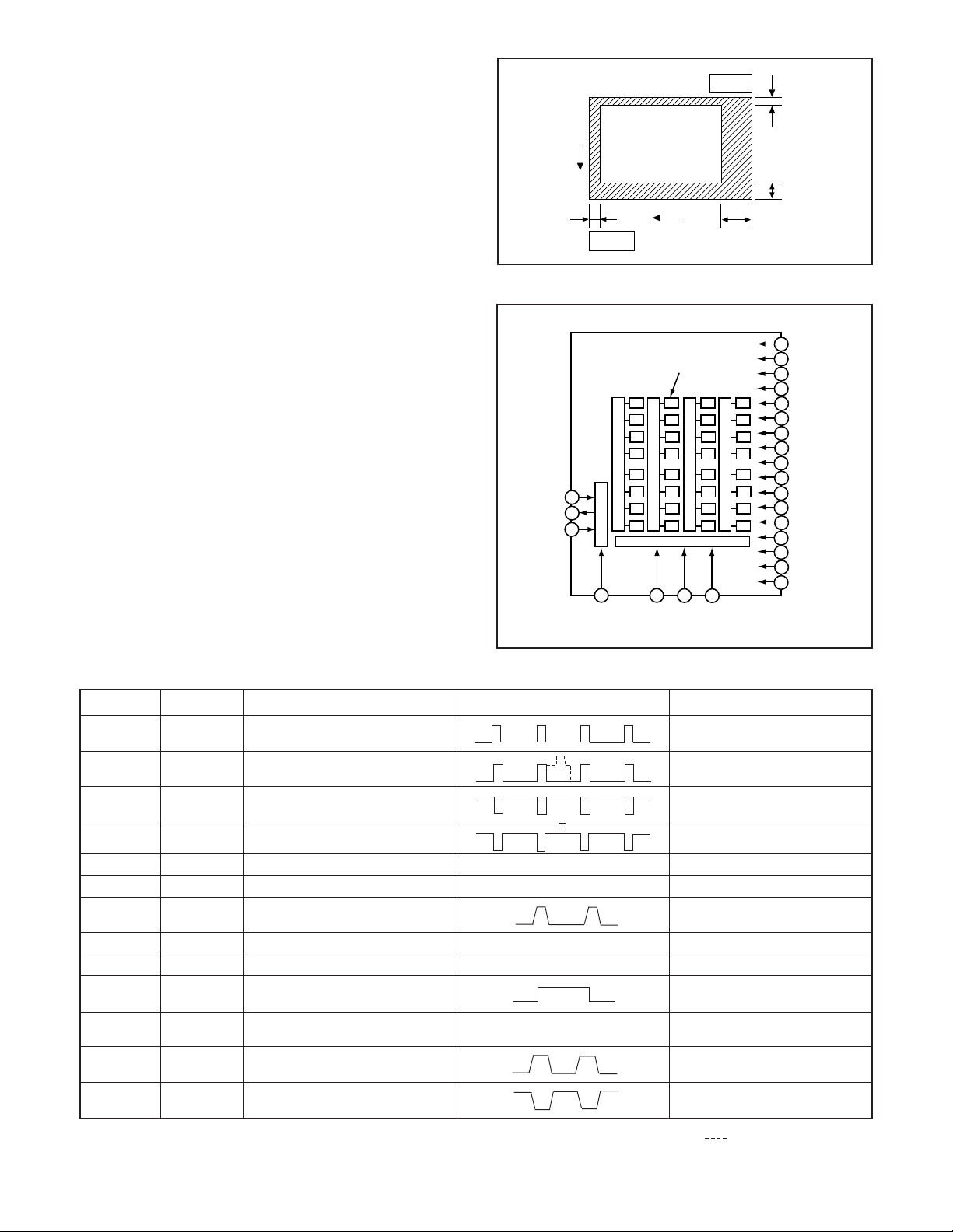
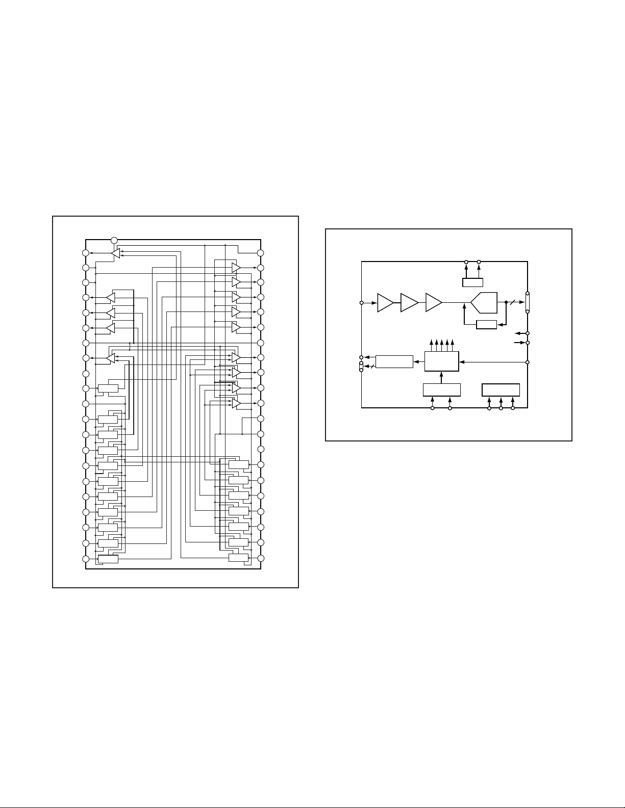
2. IC903 (CCD)
[Structure]
Interline type CCD image sensor
Optical size 1/2.5 type format
Effective pixels 2864 (H) X 2160 (V)
Pixels in total 2934 (H) X 2171 (V)
Optical black
Horizontal (H) direction: Front 12 pixels, Rear 58 pixels
Vertical (V) direction: Front 6 pixels, Rear 5 pixels
Dummy bit number Horizontal : 28 Vertical :7
Pin No.
Symbol Pin Description
Fig. 1-1.Optical Black Location (Top View)
Photo diode
10
VDD
VO
GND
13
14
15
Vertical shift register
Output part
Horizontal shift register
16
RG
ø
20
21
22
H2
H1
HL
ø
ø
ø
11
12
23
24
17
18
19
Fig. 1-2. CCD Block Diagram
Waveform
Voltag e
ø
1
ø
2
ø
3
ø
4
ø
5
ø
6
ø
7
ø
8
9
ø
ø
ø
GND
ø
ø
PT
SUBSW
ø
V6
V5B
V5A
V4
V3B
V3A
V3L
V3R
V2
V1
V1S
V5R
V5L
Vsub
1, 23, 24
2, 3
4, 7, 8, 9, 11
5, 6, 10
14
13
16
12, 15
17
18
19
20, 21
22
6, V5R , V5L
V
V
5B, V5A Vertical register transfer clock
V4, V3L, V3R,
V2, V1S
V
3B, V3A, V1
VO
VDD
ØRG
GND
PT
Vertical register transfer clock
Vertical register transfer clock
Vertical register transfer clock
Signal output
Circuit power
Reset gate clock
GND
Protection transister bias
Substrate controlSUB SW
SUB
L, H1
H
H
Substrate clock
Horizontal register transfer clock
Horizontal register transfer clock
2
Table 1-1. CCD Pin Description
-6.0 V, 0 V
-6.0 V, 0 V, 12 V
-6.0 V, 0 V
-6.0 V, 0 V, 12 V
DC
DC
Aprox. 12 V
12 V
4.5 V, 7.8 V
GND 0 V
DC
-6.0 V
0, 3.3 V (When importing all
picture element: 3.3 V)
DC
Aprox. 6 V
(Different from every CCD)
0 V, 3.3 V
0 V, 3.3 V
When sensor read-out
– 3 –
Page 3
3. Part of IC905 (H Driver) and IC901 (V Driver)
An H driver (part of IC905) and V driver (IC901) are necessary in order to generate the clocks (vertical transfer clock,
horizontal transfer clock and electronic shutter clock) which
driver the CCD.
IC905 has the generation of horizontal transfer clock and the
function of H driver, and is an inverter IC which drives the
horizontal CCDs (H1 and H2). In addition the XV1-XV6 signals which are output from IC101 are vertical transfer clocks,
and the XSG signal is superimposed onto XV1, XV3 and XV5
at IC901 in order to generate a ternary pulse. In addition, the
XSUB signal which is output from IC101 is used as the sweep
pulse for the electronic shutter, and the RG signal which is
output from IC905 is the reset gate clock.
VMSUB
9
3-level
OSUB
VM
OV1
RESET
SUBCNT
VDC
CH1
V5R
V5L
V3R
V3L
V1S
10
VL
5
VL
27
2-level
24OV2
2-level
23OV4
2-level
21OV6
8
3-level
20
28
Level
1
conversion
3
Level
32
conversion
Level
V1
33
conversion
Level
31
V6
conversion
Level
V4
30
conversion
Level
29
V2
conversion
Level
37
conversion
Level
38
conversion
Level
35
conversion
Level
36
conversion
Level
34
conversion
2-level
2-level
2-level
2-level
2-level
3-level
3-level
3-level
3-level
Level
conversion
Level
conversion
Level
conversion
Level
conversion
Level
conversion
Level
conversion
Level
conversion
7
VHH
16
OV5R
15
OV5L
18
OV3R
17
OV3L
19
OV1S
25
VM
12
OV5A
11
OV5B
14
OV3A
13
OV3B
6
VH
26
VH
4
GND
41
CH2
40
V3
39
CH4
44
CH3
43
V5
42
CH5
2
SUB
4. IC905 (H Driver, CDS, AGC and A/D converter)
IC905 contains the functions of H driver, CDS, AGC and A/D
converter. As horizontal clock driver for CCD image sensor,
HØ1 (A and B) and HØ2 (A and B) are generated inside, and
output to CCD.
The video signal which is output from the CCD is input to pins
(27) of IC905. There are sampling hold blocks generated from
the SHP and SHD pulses, and it is here that CDS (correlated
double sampling) is carried out.
After passing through the CDS circuit, the signal passes
through the AGC amplifier (VGA: Variable Gain Amplifier). It
is A/D converted internally into a 10-bit signal, and is then
input to ASIC (IC101). The gain of the VGA amplifier is controlled by pin (31)-(33) serial signal which is output from ASIC
(IC101).
REFB
REFT
VREF
ADC
INTERNAL
REGISTERS
SL
SCK
10
SDATA
DOUT
HBLK
CLP/PBLK
CLI
10-BIT
CLAMP
VD
CCDIN
RG
H1-H4
6~42 dB
0~18 dB
VGA
PxGA
CDS
INTERNAL
CLOCKS
HORIZONTAL
4
DRIVERS
AD9948
PRECISION
TIMING
CORE
SYNC
GENERATOR
HD
Fig. 1-4. IC905 Block Diagram
Fig. 1-3. IC901 Block Diagram
– 4 –
Page 4

1-2. CP1 CIRCUIT DESCRIPTION
1. Circuit Description
1-1. Digital clamp
The optical black section of the CCD extracts averaged values from the subsequent data to make the black level of the
CCD output data uniform for each line. The optical black section of the CCD averaged value for each line is taken as the
sum of the value for the previous line multiplied by the coefficient k and the value for the current line multiplied by the
coefficient (k-1).
1-2. Signal processor
1. γ correction circuit
This circuit performs (gamma) correction in order to maintain
a linear relationship between the light input to the camera
and the light output from the picture screen.
2. Color generation circuit
This circuit converts the CCD data into RGB signals.
3. Matrix circuit
This circuit generates the Y signals, R-Y signals and B-Y signals from the RGB signals.
2. Outline of Operation
When the shutter opens, the reset signals and the serial signals (“take a picture” commands) from the 8-bit microprocessor are input to ASIC (IC101) and operation starts. When the
TG/SG drives the CCD, picture data passes through the A/D
and CDS, and is then input to the ASIC as 12-bit data. The
AF, AE, AWB, shutter, and AGC value are computed from this
data, and three exposures are made to obtain the optimum
picture. The data which has already been stored in the SDRAM
is read by the CPU and color generation is carried out. Each
pixel is interpolated from the surrounding data as being either R, G and B primary color data to produce R, G and B
data. At this time, correction of the lens distortion which is a
characteristic of wide-angle lenses is carried out. After AWB
and γ processing are carried out, a matrix is generated and
aperture correction is carried out for the Y signal, and the
data is then compressed by the JPEG method by (JPEG) and
is then written to card memory (SD card).
When the data is to be output to an external device, it is taken
data from the memory and output via the USB. When played
back on the LCD and monitor, data is transferred from memery
to the SDRAM, and the data elongated by JPEG decorder is
displayed over the SDRAM display area.
4. Horizontal and vertical aperture circuit
This circuit is used gemerate the aperture signal.
1-3. AE/AWB and AF computing circuit
The AE/AWB carries out computation based on a 256-segment screen, and the AF carries out computations based on
a 11-segment screen.
1-4. SDRAM controller
This circuit outputs address, RAS, CAS and AS data for controlling the SDRAM. It also refreshes the SDRAM.
1-5. Communication control
1. SIO
This is the interface for the 8-bit microprocessor.
2. PIO/PWM/SIO for LCD
8-bit parallel input and output makes it possible to switch between individual input/output and PWM input/output. It is prepared for 16-bit parallel output.
1-6. TG/SG
Timing generated for 6 million pixel CCD control.
1-7. Digital encorder
It generates chroma signal from color difference signal.
1-8. JPEG encorder and decorder
It is compressed and elongated the data by JPEG system.
3. LCD Block
LCD block is in the CP1 board, and it is constructed by VCOM
generation circuit etc. The video signal from the ASIC are 8bit digital signal, and input to LCD directly. It is converted into
RGB signals at driver circuit in the LCD.
The VCOM (common polar voltage: AC) and the R, G and B
signals becomes greater, the display becomes darker; if the
difference in potential is smaller, the element opens and the
LCD become brighter. And also the timing pulse except the
video signal is input to LCD directly from ASIC.
4. Lens drive block
4-1. Shutter drive
The shutter drive signal (SIN1 and SIN2) which is output from
the ASIC is drived the shutter constant level driver (IC951),
and then shutter is opened and closed.
4-2. Iris drive
The iris stepping motor drive signals (IIN1 and IIN2) which
are output from the ASIC (IC101) are used to drive by the
motor driver (IC951).
4-3. Focus drive
The focus stepping motor drive signals (FIN1, FIN2, FIN3 and
FIN4) which are output from the ASIC (IC101) are used to
drive by the motor driver (IC951). Detection of the standard
focusing positions is carried out by means of the
photointerruptor (AFPI) inside the lens block.
4-4. Zoom drive
The zoom DC motor drive signals (ZIN1 and ZIN2) which are
output from the ASIC (IC101) are used to drive by the motor
driver (IC951). Detection of the zoom positions is carried out
by means of photoreflector (ZMPI) inside the lens block.
– 5 –
Page 5

1-3. PWA POWER CIRCUIT DESCRIPTION
1. Outline
This is the main power circuit, and is comprised of the following blocks.
Switching controller (IC501)
Analog system power output (L5001, Q5001)
5 V power output (L5014, Q5008)
Digital 3.25 V power output (L5006)
Digital 1.2 V power output (L5007)
LCD 15 V system power output (L5005, Q5004)
Backlight power output (L5008, Q5009)
Motor system power output (IC531, L5301, Q5301)
2. Switching Controller (IC501)
This is the basic circuit which is necessary for controlling the
power supply for a PWM-type switching regulator, and is provided with seven built-in channels, only CH1 (digital system
1.2 V), CH2 (digital 3.25 V), CH4 (LCD 15 V system), CH5
(analog system), CH6 (backlight system) and CH7 (5 V system) are used. Feedback from digital system 1.2 V (D) (CH1),
3.25 V (D) (CH2), LCD 15 V system (CH4), analog system
(CH5), backlight system (CH6) and 5 V system (CH7) power
supply outputs are received, and the PWM duty is varied so
that each one is maintained at the correct voltage setting level.
Feedback for the backlight power (CH6) is provided to the
both ends voltage of registance so that regular current can
be controlled to be current that was setting.
2-1. Short-circuit protection circuit
If output is short-circuited for the length of time determined
by internal fixing of IC501 , all output is turned off. The control
signal (P ON) are recontrolled to restore output.
3. Analog System Power Output
+12 V (A), +3.45 V (A) and -6.0 V (A) are output. Feedback for
the +12 V (A) is provided to the switching controller (Pin (4) of
IC501) so that PWM control can be carried out.
4. Digital 3.25 V Power Output
VDD3 is output. Feedback for the VDD3 is provided to the
swiching controller (Pin (54) of IC501) so that PWM control
can be carried out.
5. Digital 1.2 V Power Output
VDD1.2 is output. Feedback for the VDD1.2 is provided to the
switching controller (Pin (52) of IC501) so that PWM control
to be carried out.
6. 5 V System Power Output
5 V is output. Feedback for the 5 V output is provided to the
switching controller (Pin (9) of IC501) so that PWM control to
be carried out.
7. LCD System Power Output
+15 V (L) is output. Feedback for the +15 V (L) is provided to
the switching controller (Pin (2) of IC501) so that PWM control to be carried out.
8. Backlight Power Output
Regular current is being transmitted to LED for LCD backlight. Feedback for the both ends voltage of registance that is
being positioned to in series LED are provided to the switching controller (Pin (6) of IC501) so that PWM control to be
carried out.
9. Motor System Power Output
3.6 V is output. Feedback for the 3.6 V output is sent to pin (1)
of IC531 for PWM control to be carried out.
– 6 –
Page 6

1-4. STA STROBE CIRCUIT DESCRIPTION
1. Charging Circuit
When UNREG power is supplied to the charge circuit and the
CHG signal from microprocessor becomes High (3.3 V), the
charging circuit starts operating and the main electorolytic
capacitor is charged with high-voltage direct current.
However, when the CHG signal is Low (0 V), the charging
circuit does not operate.
1-1. Charging switch
The CHG signal becomes High, Q5406 becomes ON and the
charging circuit starts operating.
1-2. Power supply filter
C5406 constitutes the power supply filter. They smooth out
ripples in the current which accompany the switching of the
oscillation transformer.
1-3. Oscillation circuit
This circuit generates an AC voltage (pulse) in order to increase the UNREG power supply voltage when drops in current occur. This circuit generates a drive pulse with a frequency
of approximately 50-100 kHz. Because self-excited light omission is used, the oscillation frequency changes according to
the drive conditions.
2. Light Emission Circuit
When FLCLT signals are input from the ASIC expansion port,
the stroboscope emits light.
2-1. Emission control circuit
When the FLCLT signal is input to Hi at the emission control
circuit, Q5409 switches on and preparation is made to the
light emitting. Moreover, when a FLCLT signal becomes Lo,
the stroboscope stops emitting light.
2-2. Trigger circuit
The Q5409 is turned ON by the FLCLT signal and light emission preparation is preformed. Simultaneously, high voltage
pulses of several kV are emitted from the trigger coil and applied to the light emitter.
2-3. Light emitting element
When the high-voltage pulse form the trigger circuit is applied to the light emitting part, currnet flows to the light emitting element and light is emitted.
Beware of electric shocks.
1-4. Oscillation transformer
The low-voltage alternating current which is generated by the
oscillation control circuit is converted to a high-voltage alternating current by the oscillation transformer.
1-5. Rectifier circuit
The high-voltage alternating current which is generated at
the secondary side of T5401 is rectified to produce a highvoltage direct current and is accumulated at electrolytic capacitor C5412.
1-6. Voltage monitoring circuit
This circuit is used to maintain the voltage accumulated at
C5412 at a constance level.
After the charging voltage is divided and converted to a lower
voltage by R5405 and R5406, it is output as the monitoring
voltage VMONIT. When VMONIT voltage reaches a specified
level, the CHG signal is switched to Low and charging is interrupted.
– 7 –
Page 7

1-5. SYA CIRCUIT DESCRIPTION
1. Configuration and Functions
For the overall configuration of the SYA block, refer to the block diagram. The SYA block centers around a 8-bit microprocessor
(IC301), and controls camera system condition (mode).
The 8-bit microprocessor handles the following functions.
1. Operation key input, 2. Clock control and backup, 3. Power ON/OFF, 4. Storobe charge control, 5. Signal input and output for
zoom and lens control.
Pin
1
2
3
4
5
6
7
8
9
10
11
12
13
14
15
16
17
18
19
20
21 SI
22 SCK
23 AVREF
24
25 VMONIT
26
27
28
29
30
31
32
33
34
35
36
37
38
39
40
41
Signal
MRST
BUCKUP CTL
SCAN IN1
SCAN OUT0
SCAN OUT1
SCAN OUT2
COMREQ
HOT LINE
BL ON
LCD ON3
LCD ON
P ON
CHG ON
ZSREQ
TSEN PULSE
LCD PWM
VF LED
RxD6
TxD6
SO
AVSS
BATTERY
T. SEN VOUT
AV JACK
ZUSBDET
ZDC IN
CARD
SCAN OUT3
PLLEN
SCAN IN0
SCAN IN2
SCAN IN3
BATT OFF
AVREF ON
SELF PRG
RESET
XCOUT
I/O
O
O
O
O
O
O
O
O
O
O
O
O
O
O
O
O
O
O
O
O
O
O
Outline
System reset
Backup battery charge control
I
I
I
I
I
I
-
I
I
I
I
I
I
I
I
I
I
I
I
Key matrix input
Key matrix output
Key matrix output
Key matrix output
Command request
Direct-coupled line to ASIC
Backlight ON/OFF
D/D converter (LCD system) ON/OFF signal 3
D/D converter (LCD system) ON/OFF signal
D/D converter (digital system) ON/OFF signal 3
Strobe charge control
SREQ
Touch sensor pulse output
-
VF LED (L= lighting)
UART receiving for writing
UART transmission for writing
Serial data output
Serial data input
Serial clock output
Analog standard voltage input terminal
GND
Main condensor charge voltage detection
Battery voltage detection
Touch sensor voltage input
AV jack detection
USB connector detection
External power detection
SD card detection
Keymatrix output
PLL oscillation ON/OFF
Keymatrix input
Keymatrix input
Keymatrix input
Battery OFF detection signal input
AD VREF ON/OFF signal
Writing control
Reset input
Clock oscillation terminal for clock
See next page
– 8 –
Page 8

42
43
44
45
46
47
48
XCIN I
FLMDO O Microprocessor Port
XOUT
XIN I Main clock oscillation terminal (not used)
VREF - Standard voltage
VSS - GND
VDD I VDD
O
Table 5-1. 8-bit Microprocessor Port Specification
Clock oscillation terminal for clock (32.768 kHz)
Main clock oscillation terminal (not used)
2. Internal Communication Bus
The SYA block carries out overall control of camera operation by detecting the input from the keyboard and the condition of the
camera circuits. The 8-bit microprocessor reads the signals from each sensor element as input data and outputs this data to the
camera circuits (ASIC) or to the LCD display device as operation mode setting data. Fig. 5-1 shows the internal communication
between the 8-bit microprocessor and ASIC.
8-bit micro processor ASIC
setting of
external port
communication
Fig. 5-1 Internal Bus Communication System
MRST
HOT LINE
PLLEN
SCK
SREQ
COMREQ
3. Key Operaiton
For details of the key operation, refer to the instruction manual.
SCAN
OUT
SCAN
IN
0
1
2
3
0
-
RIGHT
UP
-
1
S1
DOWN
LEFT
WIDE
2
S2
SET
MENU
TELE
SI
SO
3
PW_ON
-
-
PLAY
Table 5-2. Key Operation
– 9 –
Page 9

4. Power Supply Control
The 8-bit microprocessor controls the power supply for the overall system.
The following is a description of how the power supply is turned on and off. When the battery is attached, IC955 is operating and
creating 3.6 V, a regulated 3.2 V voltage is normally input to the 8-bit microprocessor (IC301) by IC302, clock counting and key
scanning is carried out even when the power switch is turned off, so that the camera can start up again.
When the power switch is off, the 8-bit microprocessor halts 8 MHz of the main clock, and operates 32.768 kHz of subclock.
When the battery is removed, the 8-bit microprocessor power switches the lithum secondary battery for memory backup by
IC302, and operates at low consumption. At this condition, the 8-bit microprocessor halts 8 MHz of the main clock, and operates
32.768 kHz clock counting by subclock.
Also, the battery for backup is charged 16 hours from it to be attached.
When the power switch is on, the 8-bit microprocessor starts processing. The 8-bit microprocessor first sets both the PON signal
at pin (12) and the PAON signal (ASIC) to High, and then turn on the power circuit. After PON signal is to High, sets external port
of ASIC after approximately 100 ms. According to setting of this external port, carry out setting of the operating frequency and
oscillation control in the ASIC. Also, it starts communication with ASIC, and confirms the system is operative.
When the through image is operating, set the PAON signal (ASIC) to High and then turn on the CCD. When the through image is
playing, set the PAON signal to Low and then turn off the CCD. When LCD panel turns on, set LCD ON signal at pin (11) and LCD
ON3 signal at pin (10) to High, and then turn on the power. Set BL ON signal at pin (9) to High, and turn on the backlight power.
When the power switch is off, the lens will be stowed, and PON, PAON, LCDON and BLON signals to Low and the power supply
to the whole system is halted. The 8-bit microprocessor halts oscillation of the main clock (8 MHz), and set operation mode of
clock ocillation.
Power supply voltage
Power OFF
Playback mode
Shooting mode (LCD)
Shooting mode (OVF)
Shooting
USB connection
ASIC,
memory
1.50 V, 3.25 V
OFF
ON
ON
OFF
ON
ON
Table 5-3. Power supply control
CCD
12 V, -6 V
3.45 V
OFF
OFF
OFF
OFF
ON
OFF
8bit
CPU
3.2 V
32KHz
8MHz
8MHz
8MHz
8MHz
8MHz
LCD
MONITOR
15 V, 5.0 V
OFF
ON
ON
OFF
ON
OFF
– 10 –
Page 10

2. DISASSEMBLY
2-1. REMOVAL OF CABI BACK
1. Two screws 1.7 x 6
2. Open the cover battery.
3. Screw 1.7 x 4
4. Cabinet bottom
5. Cover battery
6. Stand
7. Three screws 1.7 x 4
8. Two screws 1.7 x 3
9. Cabi back
10. Screw 1.7 x 4
15
8
11. Screw 1.7 x 4
12. Screw 1.7 x 3
13. Screw 1.7 x 2
14. Cabinet top & Cabi front
15. FPC
7
9
11
7
c
3
14
2, 5
NOTE: Discharge a strobe capacitor
with the discharge jig (VJ8-0188) for
electric shock prevention.
10
a
b
4
13
12
8
6
When assembling,
tighten the screws order.
a → b → c
1
– 11 –
Page 11

2-2. REMOVAL OF LCD
1. Spacer under monitor
2. LCD
3. Remove the solder.
4. FPC
5. Two screws 1.4 x 3.5
6. Two screws 1.7 x 4
7. FPC
8. Holder monitor
9. Screw 1.7 x 2
10. Spring earth CP1
11. Unit, sw FPC
7
1
11
8
2
9
5
10
6
6
4
3
– 12 –
Page 12

2-3. REMOVAL OF CP1 BOARD AND LENS ASSEMBLY
1. Remove the solder.
2. Buzzer
3. Remove the solder.
4. Remove the solder.
5. Spacer trigger
6. Remove the solder.
7. Remove the solder.
8. Screw 1.7 x 4
22
21
9. CP1 board
10. Remove the solder.
11. Condensor
12. FPC
13. Three screws 1.4 x 3.5
14. Lens assembly
15. Assy flash
16. Spacer battery
11
20
10
17. Two screws 1.7 x 3
18. Holder strap
19. Dec self LED
20. Spacer fuse
21. Remove the solder.
22. Assy, wire batt +
23. Terminal batt A
24. Holder chassis
1
4
B
D
7
B
C
13
A
B
B
6
B
12
b
a
c
23
17
18
15
16
8
3
5
B
D
BC
A
19
14
When assembling,
tighten the screws order.
a → b → c
9
24
2
– 13 –
Page 13

2-4. REMOVAL OF CABI FRONT AND TB1 BOARD
1. Three screws 1.7 x 3
2. Cabinet top
3. Cabi front
4. Spacer flash
5. Screw 1.7 x 2.5
6. Shield tape TB1
7. Screw 1.7 x 2.5
8. TB1 board
9. Spring shutter
10. Dec top LED
11. Button shutter
12. Button power
11
2
1
10
12
9
6
8
5
7
4
3
– 14 –
Page 14

2-5. BOARD LOCATION
TB1 board
CP1 board
– 15 –
 Loading...