

Page 1

WARNING
Do not use solder containing lead.
This product has been manufactured using lead-free solder in
order to help preserve the environment.
Because of this, be sure to use lead-free solder when carrying
out repair work, and never use solder containing lead.
Lead-free solder has a melting point that is 30 - 40°C (86 104°F) higher than solder containing lead, and moreover it does
not contain lead which attaches easily to other metals. As a
result, it does not melt as easily as solder containing lead, and
soldering will be more difficult even if the temperature of the
soldering iron is increased.
The extra difficulty in soldering means that soldering time will
increase and damage to the components or the circuit board
may easily occur.
Because of this, you should use a soldering iron and solder
that satisfy the following conditions when carrying out repair
work.
Soldering iron
Use a soldering iron which is 70 W or equivalent, and which
lets you adjust the tip temperature up to 450°C (842°F). It
should also have as good temperature recovery characteristics as possible.
Set the temperature to 350°C (662°F) or less for chip components, to 380°C (716°F) for lead wires and similar, and to 420°C
(788°F) when installing and removing shield plates.
The tip of the soldering iron should have a C-cut shape or a
driver shape so that it can contact the circuit board as flat or in
a line as much as possible.
Note:
If replacing existing solder containing lead with lead-free solder in the soldered parts of products that have been manufactured up until now, remove all of the existing solder at those
parts before applying the lead-free solder.
Solder
Use solder with the metal content and composition ratio by
weight given in the table below. Do not use solders which do
not meet these conditions.
Metal content
Composition
ratio by weight
Lead-free solder is available for purchase as a service tool.
Use the following part number when ordering:
Part name: Lead-free solder with resin (0.5 mm dia., 500 g)
Part number: VJ8-0270
Tin (Sn) Silver (Ag)
96.5 %
3.0 %
Copper (Cu)
0.5 %
– 2 –
Page 2
1. OUTLINE OF CIRCUIT DESCRIPTION
1-1. CCD CIRCUIT DESCRIPTION
1. IC Configuration
The CCD peripheral circuit block basically consists of the following ICs.
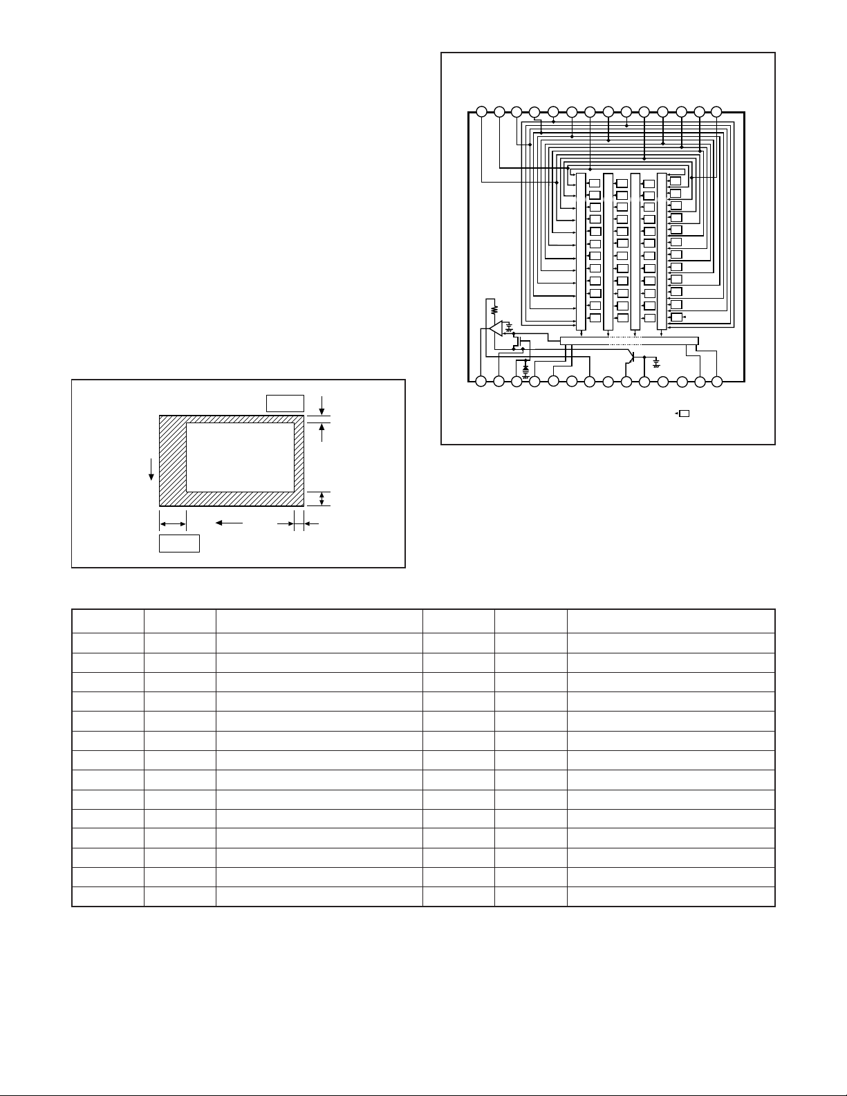
IC903 (ICX624AQN) CCD imager
IC901 (CXD3443GA) V driver
IC905 (AD9949AKCP) CDS, AGC, A/D converter, H driver
2. IC903 (CCD)
Interline type CCD image sensor
Optical size 1/2.5 type
Effective pixels 2840 (H) x 2128 (V)
Pixels in total 2892 (H) x 2138 (V)
Optical black
Horizontal (H) direction: Front 48 pixels, Rear 4 pixels
Vertical (V) direction: Front 8 pixels, Rear 2 pixels
Dummy bit number Horizontal : 28
Pin 1
2
Ø7A
V
RG
Ø
ØHLD
Ø6
V
V
10
9
11
19
20
18
Ø2B
Ø1B
H
H
Ø7B
Ø8
V
V
14
13
12
16
15
17
DD
OUT
V
V
Ø5A
Ø5B
V
V
7
8
G
R
G
R
G
R
G
R
Vertical register
G
R
G
R
Horizontal register
21
22
GND
GND
Ø4
V
GND
B
G
B
G
B
G
B
G
B
G
B
G
23
Ø3A
Ø3B
ØST
V
V
V
6
4
5
G
R
G
R
G
R
G
R
G
R
G
R
25
24
NC
SUB
SUB
C
Ø
(Note) : Photo sensor
Ø1A
Ø1B
Ø2
V
V
V
1
3
2
B
G
B
G
B
G
B
G
B
G
B
(Note)
G
28
26
27
L
V
Ø2A
Ø1A
H
H
V
48
Pin 15
H
Fig. 1-1.Optical Black Location (Top View)
Pin No.
1
2
3
4
5
6
7
8
9
10
11
12
13
14
Symbol
1A
Vø
Vø1B
Vø2
Vø3A
Vø3B
VøST
Vø4
Vø5A
Vø5B
VøHLD
6
Vø
7A
Vø
Vø7B
Vø8
Pin Description
Vertical register transfer clock
Vertical register transfer clock
Vertical register transfer clock
Vertical register transfer clock
Vertical register transfer clock
Horizontal addition control clock
Vertical register transfer clock
Vertical register transfer clock
Vertical register transfer clock
Horizontal addition control clock
Vertical register transfer clock
Vertical register transfer clock
Vertical register transfer clock
Vertical register transfer clock
Fig. 1-2. CCD Block Diagram
8
4
Pin No.
15
16
17
18
19
20
21
22
23
24
25
26
27
28
Symbol
OUT
V
VDD
øRG
1B
Hø
Hø2B
GND
GND
Horizontal register transfer clock
Horizontal register transfer clock
GND
GND
GND GND
øSUB
C
SUB
NC
L
V
1A
Hø
Hø2A
Substrate clock
Substrate bias
-
Protection transistor bias
Horizontal register transfer clock
Horizontal register transfer clock
Signal output
Circuit power
Reset gate clock
Pin Description
Table 1-1. CCD Pin Description
– 3 –
Page 3
3. IC905 (H Driver) and IC901 (V Driver)
An H driver (a part of IC905) and V driver (IC901) are necessary in order to generate the clocks (vertical transfer clock,
horizontal transfer clock and electronic shutter clock) which
driver the CCD.
IC905 has clock generating which drives horizontal CCD and
its drives function. These clocks are output from pin (14), (15),
(18) and (19) of IC905. In addition the XV1-XV8 signals which
are output from IC101 are the vertical transfer clocks, and the
XSG1A, XSG1B, XSG3A, XSG3B, XSG5A, XSG5B, XSG7A
and XSG7B signals which are output is superimposed onto
XV1, XV3, XV5 and XV7 at IC901 in order to generate a ternary pulse. In addition, the XSUB signal which is output from
IC101 is used as the sweep pulse for the electronic shutter,
and the RG signal which is output from pin (21) of IC905 is
the reset gate clock.
4. IC905 (CDS, AGC Circuit and A/D Converter)
The video signal which is output from the CCD is input to
pins (27) of IC905. There are S/H blocks inside IC905 generated from the XSHP and XSHD pulses, and it is here that
CDS (correlated double sampling) is carried out.
After passing through the CDS circuit, the signal passes
through the AGC amplifier. It is A/C converted internally into
a 12-bit signal, and is then input to IC101 of the CP1 circuit
board. The gain of the AGC amplifier is controlled by pin (31)(33) serial signal which is output from IC101 of the CP1 board.
VRB
VRT
VREF
12-BIT
ADC
12
DOUT
CCDIN
CDS
0~18 dB
PxGA
6~42 dB
VGA
DVD1
AVD1
AVS1
XSUBN
XSG9N
XV2N
XSG7N
XV7N
XSG5N
XV5N
XV3N
XSG3N
XV1N
XSG1N
XV4N
XV9N
XSG10N
XV6N
XSG8N
XV14N
XSG6N
XV13N
XV12N
XSG4N
XV11N
XSG2N
XV8N
XV10N
AVS2
AVD2
DVD2
C1
L2
L3
B1
D1
D2
E1
E2
F1
F2
G10
F11
F10
E11
E10
D11
K9
K11
J11
J10
H11
H10
G2
H1
H2
J1
J2
K1
B11
C11
L10
Input Buffer
A4
A6
A10
C2
A2
B4
A5
B6
A8
B8
A9
C10
B9
B7
A7
B5
A3
B3
L4
L5
L7
VL2
VH2
VM2
SUB
V2
V7A
V5A
V3A
V1A
V4
V9
V6
V7B
V5B
V3B
V1B
V8
V10
VM1
VH1
VL1
RG
H1-H4
INTERNAL
CLOCKS
HORIZONTAL
4
DRIVERS
AD9949
PRECISION
TIMING
CORE
SYNC
GENERATOR
VD
HD
Fig. 1-4. IC905 Block Diagram
CLAMP
INTERNAL
REGISTERS
SL
SCK
HBLK
CLP/PBLK
CLI
SDATA
Fig. 1-3. IC901 Block Diagram
– 4 –
Page 4

1-2. CP1 CIRCUIT DESCRIPTION
1. Circuit Description
1-1. Digital clamp
The optical black section of the CCD extracts averaged values from the subsequent data to make the black level of the
CCD output data uniform for each line. The optical black section of the CCD averaged value for each line is taken as the
sum of the value for the previous line multiplied by the coefficient k and the value for the current line multiplied by the
coefficient (k-1).
1-2. Signal processor
1. γ correction circuit
This circuit performs (gamma) correction in order to maintain
a linear relationship between the light input to the camera
and the light output from the picture screen.
2. Color generation circuit
This circuit converts the CCD data into RGB signals.
3. Matrix circuit
This circuit generates the Y signals, R-Y signals and B-Y signals from the RGB signals.
4. Horizontal and vertical aperture circuit
This circuit is used gemerate the aperture signal.
1-3. AE/AWB and AF computing circuit
The AE/AWB carries out computation based on a 256-segment screen, and the AF carries out computations based on
a 11-segment screen.
1-4. SDRAM controller
This circuit outputs address, RAS, CAS and AS data for controlling the SDRAM. It also refreshes the SDRAM.
1-5. Communication control
1. SIO
This is the interface for the 8-bit microprocessor.
2. PIO/PWM/SIO for LCD
8-bit parallel input and output makes it possible to switch between individual input/output and PWM input/output. It is prepared for 16-bit parallel output.
2. Outline of Operation
When the shutter opens, the serial signals (“take a picture”
commands) from the 8-bit microprocessor is input to ASIC
(IC101) and operation starts. When the TG/SG drives the CCD,
picture data passes through the A/D and CDS, and is then
input to the ASIC as 12-bit data. The AF, AE, AWB, shutter,
and AGC value are computed from this data, and three exposures are made to obtain the optimum picture. The data which
has already been stored in the SDRAM is read by the CPU
and color generation is carried out. Each pixel is interpolated
from the surrounding data as being either R, G and B primary
color data to produce R, G and B data. At this time, correction
of the lens distortion which is a characteristic of wide-angle
lenses is carried out. After AWB and γ processing are carried
out, a matrix is generated and aperture correction is carried
out for the Y signal, and the data is then compressed by the
JPEG method by (JPEG) and is then written to card memory
(SD card).
When the data is to be output to an external device, it is taken
data from the memory and output via the USB. When played
back on the LCD and monitor, data is transferred from memery
to the SDRAM, and the data elongated by JPEG decorder is
displayed over the SDRAM display area.
3. LCD Block
The LCD display circuit is located on the CP1 board, and
consists of components such as a power circuit and VCOM
control circuit.
The signals from the ASIC are 8-bit digital signals, that is
input to the LCD directly. The 8-bit digital signals are converted to RGB signals inside the LCD driver circuit . LCD is
input signals from ASIC directly to the LCD, and function such
as image quality are controlled.
Because the LCD closes more as the difference in potential
between the VCOM (common polar voltage: AC) and the R,
G and B signals becomes greater, the display becomes darker;
if the difference in potential is smaller, the element opens and
the LCD become brighter.
In addition, the timing pulses for signals other than the video
signals are also input from the ASIC directory to the LCD.
1-6. TG/SG
Timing generated for 6 million pixel CCD control.
1-7. Digital encorder
It generates chroma signal from color difference signal.
1-8. JPEG encorder and decorder
It is compressed and elongated the data by JPEG system.
– 5 –
Page 5

4. Lens drive block
4-1. Shutter drive
The shutter drive signals (SIN1 and SIN2) which are output
from the ASIC are used to drive (SHUT (+) and SHUT (–))
the shutter constant level driver (IC951), and then shutter is
opened and closed.
4-2. Iris drive
The iris stepping motor drive signals (IIN1 and IIN2) which
are output from the ASIC (IC101) are used to drive (IRIS (+)
and IRIS (–)) by the motor driver (IC951), and are then used
to drive the iris steps.
4-3. Focus drive
The focus stepping motor drive signals (FIN1, FIN2, FIN3 and
FIN4) which are output from the ASIC (IC101) are used to
drive (AFSPM (1) +A, AFSPM (2) –A, AFSPM (3) +B and
AFSPM (4) –B) by the motor driver (IC951). Detection of the
standard focusing positions is carried out by means of the
photointerruptor (AFPI) inside the lens block.
4-4. Zoom drive
The zoom DC motor drive signals (ZIN1 and ZIN2) which are
output from the ASIC (IC101) are used to drive (ZM (+) and
ZM (–)) by the motor driver (IC951). Detection of the standard
zooming positions is carried out by means of photoreflector
(ZMPR_E) inside the lens block. Getting of the zoom positions
is carried out by means of the photo-interrupter (ZMPI_E) by
ASIC (IC101) is counting inside the lens block.
– 6 –
Page 6

1-3. PWA POWER CIRCUIT DESCRIPTION
1. Outline
This is the main power circuit, and is comprised of the following blocks.
Switching power control IC (IC501)
Analog 12 V (A) output system (L5006, Q5001)
Analog -7.5 V (A) output system (L5007, Q5004, IC503)
Analog 3.25 V (A) output system (Q5009)
Digital 3.25 V (D) output system (L5003)
Digital 1.20 V (D) output system (L5004)
Backlight output system (L5005, Q5002)
Boost power (L5301)
2. Switching Power Controller (IC501)
This is the basic circuit which is necessary for controlling the
power supply for a PWM-type switching regulator, and is provided with eight built-in channels.
PWM/PFM switching step-up circuit …… 1 (ch_1)
PWM drive step-up/step-down circuit …… 1 (ch_2)
PWM drive step-up and step-down circuit …… total 4 (ch_3
and ch_5~ch_7)
PWM drive inverter circuit …… 1 (ch_4)
Variable regulator …… 1 (ch_8)
Only ch_1 (starting IC, lens drive, 8-bit microprocessor and
ch_3 source), ch_2 (digital 3.25 V), ch_3 (digital 1.20 V), ch_4
(analog -7.5 V), ch_5 (analog 12 V), ch_6 (not used), ch_7
(backlight) and ch_8 (not used) are used. Feedback from 3.6
V (ch_1), 3.25 V (ch_2), 1.20 V (ch_3), -7.5 V (ch_4) and 12.0
V (ch_5) power supply outputs are received, and the PWM
duty is varied so that each one is maintained at the correct
voltage setting level.
Feedback for the backlight power (ch_7) is provided so that
regular current can be controlled to be current (approximately
20 mA) that was setting.
PWM/PFM switching can be carried out for ch_1, so that PFM
operation is enabled when the DSC is stopped (when the
power is off) which provides greater efficiency at times of low
loads (only the 8-bit microprocessor is driven).
3. ch_1 Output System
3.6 V is output. Feedback for the 3.6 V output is provided to
the switching controller (Pin (36) of IC501) so that PWM control can be carried out.
While DSC is stopped, control switches to PFM control.
4. ch_2 Output System
3.25 V (D) is output. Feedback for the 3.25 V (D) output is
provided to the switching controller (Pin (45) of IC501) so that
PWM control can be carried out. Also, it is the source for 3.25
V (A).
5. ch_3 Output System
1.20 V (D) is output. Feedback for the 1.20 V (D) output is
provided to the swiching controller (Pin (44) of IC501) so that
PWM control can be carried out.
6. ch_4 Output System
-7.5 V is output. Feedback for the inverter circuit output is
provided to the switching power controller (Pin (38) of IC501)
so that PWM control can be carried out. This output is high
precision by IC503, and get to -7.5 V.
7. ch_5 Output System
12.0 V (A) is output. Feedback for the 12.0 V (A) is provided
to the switching power controller (Pin (39) of IC501) so that
PWM control can be carried out.
8. ch_7 Output System
Regular current is being transmitted to LED for backlight. Stepdown in the voltage from the LED are feedback to the switching power controller (Pin (42) of IC501) so that PWM control
can be carried out.
The control signal (LCD PWM) from the 8-bit system can be
used to adjust the backlight illumination.
2-1. Damage Prevention Circuit
When a short-circuit is generated for a constant period of time,
the capacitor that is connected to pin (1) of IC501 turns all
output off. It is also equipped with an overheating protection
circuit, so that when the element temperature becomes higher
than a certain temperature, all output is turned off in the same
way as for a short-circuit. To reset output, remove the cause
of the problem and then resend a control signal.
– 7 –
Page 7

1-4. CP1 STROBE CIRCUIT DESCRIPTION
1. Charging Circuit
When UNREG power is supplied to the charge circuit and the
CHG signal from microprocessor becomes High (3.3 V), the
charging circuit starts operating and the main electorolytic
capacitor is charged with high-voltage direct current.
However, when the CHG signal is Low (0 V), the charging
circuit does not operate.
1-1. Charging switch
The CHG signal becomes High, Q5404 becomes ON and the
charging circuit starts operating.
1-2. Power supply filter
C5408 constitutes the power supply filter. They smooth out
ripples in the current which accompany the switching of the
oscillation transformer.
1-3. Oscillation circuit
This circuit generates an AC voltage (pulse) in order to increase the UNREG power supply voltage when drops in current occur. This circuit generates a drive pulse with a frequency
of approximately 50-100 kHz. Because self-excited light omission is used, the oscillation frequency changes according to
the drive conditions.
2. Light Emission Circuit
When FLCLT signals are input from the ASIC expansion port,
the stroboscope emits light.
2-1. Emission control circuit
When the FLCLT signal is input to Hi at the emission control
circuit, Q5402 switches on and preparation is made to the
light emitting. Moreover, when a FLCLT signal becomes Lo,
the stroboscope stops emitting light.
2-2. Trigger circuit
The Q5402 is turned ON by the FLCLT signal and light emission preparation is preformed. Simultaneously, high voltage
pulses of several kV are emitted from the trigger coil and applied to the light emitter.
2-3. Light emitting element
When the high-voltage pulse form the trigger circuit is applied to the light emitting part, currnet flows to the light emitting element and light is emitted.
Beware of electric shocks.
1-4. Oscillation transformer
The low-voltage alternating current which is generated by the
oscillation control circuit is converted to a high-voltage alternating current by the oscillation transformer.
1-5. Rectifier circuit
The high-voltage alternating current which is generated at
the secondary side of T5401 is rectified to produce a highvoltage direct current and is accumulated at electrolytic capacitor C5412 on the main circuit board.
1-6. Voltage monitoring circuit
This circuit is used to maintain the voltage accumulated at
C5412 at a constance level.
After the charging voltage is divided and converted to a lower
voltage by R5404 and R5405, it is output as the monitoring
voltage VMONIT. When VMONIT voltage reaches a specified
level, the CHG signal is switched to Low and charging is interrupted.
– 8 –
Page 8
1-5. SYA CIRCUIT DESCRIPTION
1. Configuration and Functions
For the overall configuration of the SYA block, refer to the block diagram. The SYA block centers around a 8-bit microprocessor
(IC301), and controls camera system condition (mode).
The 8-bit microprocessor handles the following functions.
1. Operation key input, 2. Clock control and backup, 3. Power ON/OFF, 4. Storobe charge control, 5. Signal input and output for
zoom and lens control.
Pin
1
2
3
4
5
6
7
8
9
10
11
12
13
14
15
16
17
18
19
20
21 NOT USED
22 COMREQ
23 HOT LINE
24
25 SCAN IN 4
26
27
28
29
30
31
32
33
34
35
36
37
38
39
40
41
Signal
BATT_OFF
SW_3.2 V ON
NOT USED
NOT USED
CTRL
RESET
XCOUT
XCIN
FLMD0
XOUT
XIN
REGC
VSS
EVSS
VDD
EVDD
MRST
TRST
T SEN LED
SELF_LED
PLLEN
SCAN IN 3
SCAN IN 2
SCAN IN 1
SCAN IN 0
P ON
NAND_RESET
USB CONNECT
NOT USED
SCAN OUT 0
SCAN OUT 1
SCAN OUT 2
DOCK USB
ZSREQ
TSEN_PULSE
LCD PWM
BL ON
I/O
O
O
O
O
O
O
O
O
O
O
O
O
O
O
O
O
O
O
Outline
I
I
I
I
-
I
-
-
-
-
-
I
I
I
I
I
I
I
I
I
I
I
I
Battery OFF detection
SW 3.2 V line ON
-
Always low output
Lens power PFM/PWM mode switching (L= PFM, H= PWM)
Microprocessor reset terminal
Clock oscillation terminal for clock
Clock oscillation terminal for clock
Program writing control signal, mode lead-in
Main clock oscillation terminal (4 MHz)
Main clock oscillation terminal (4 MHz)
Regulator output for internal operation
GND
GND
Power terminal
Power terminal
System reset (ASIC reset)
JTAG relation reset
Touch sensor sensing LED ON
Self LED ON
-
Communication signal to ASIC
Not used. Always low output
ASIC PLL ON/OFF
Keymatrix input
Keymatrix input
Keymatrix input
Keymatrix input
Keymatrix input
D/D converter (digital system) ON/OFF
One NAND memory reset (L= reset)
USB insertion detection from CN110
Always input mode
Keymatrix output
Keymatrix output
Keymatrix output
USB insertion detection from printer dock
Communication request signal from ASIC
Clock output for touch sensor (approx. 30 kHz)
LCD backlight dimmer control signal
LCD backlight ON/OFF signal
See next page
– 9 –
Page 9
42
43
44
45
46
47
48 AVSS - Analog GND (A/D GND)
49
50
51
52
53
54
55
56
57
58
59
60
61
62
63
64
RXD6 I
TXD6 O Program writing reception data (UART)
NOT USED
NOT USED - -
NOT USED
AVREF I Internal A/D standard potential
BATTERY I Battery potential detection (A/D)
VMONIT I Strobo condensor charge potential detection (A/D)
ILLUMI I Illuminance sensor potential detection (A/D)
TOUCH_IN I Touch sensor input (A/D)
CARD I SD card insertion detection
AV JACK I AV cable insertion detection (L= detection)
NOT USED I Always input mode
NOT USED O Always low output
ST_CHG_ON O Strobo condensor charge start
SCK O Communication CLK to ASIC
SI I Reception data from ASIC
SO O Sending data to ASIC
BACKUPCTRL O Charge control to coin battery (L= charge)
FLMD0_SY O -
PW_TEST I Power compulsion ON at Low (test)
NC I Always input mode
-
-
Program writing reception data (UART)
-
-
Table 5-1. 8-bit Microprocessor Port Specification
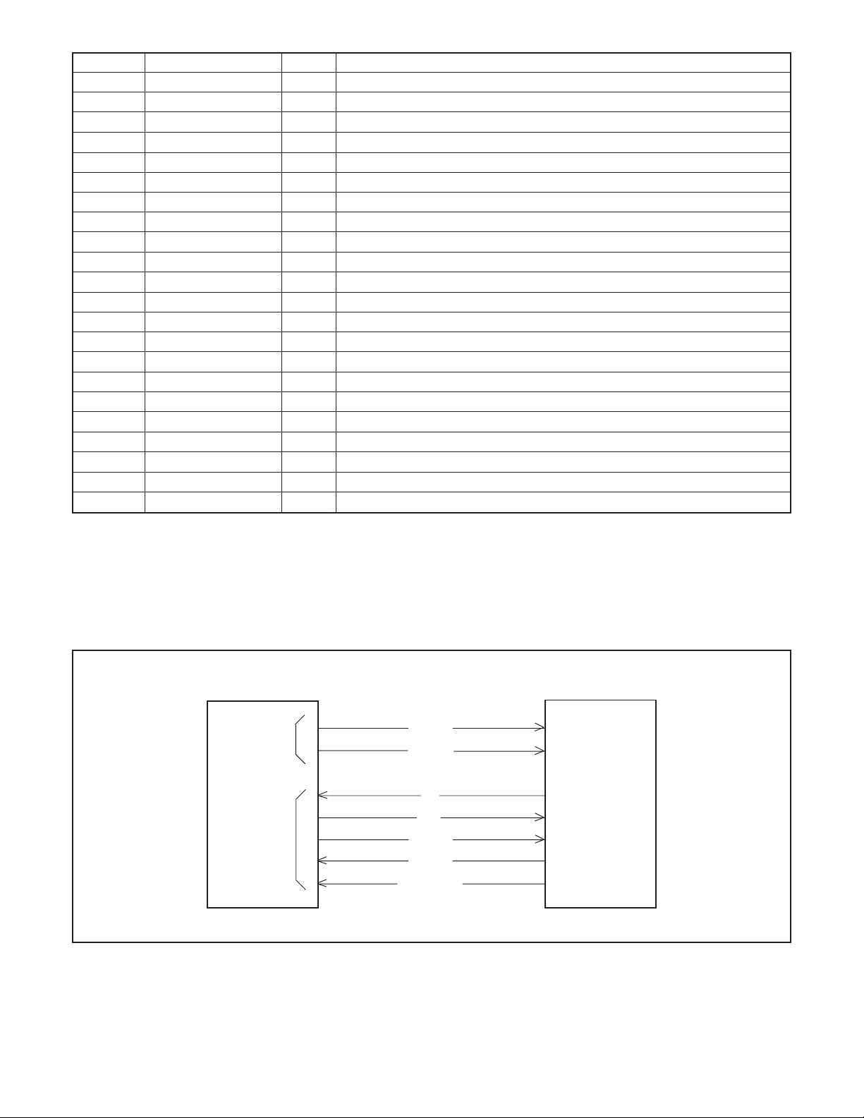
2. Internal Communication Bus
The SYA block carries out overall control of camera operation by detecting the input from the keyboard and the condition of the
camera circuits. The 8-bit microprocessor reads the signals from each sensor element as input data and outputs this data to the
camera circuits (ASIC) or to the LCD display device as operation mode setting data. Fig. 5-1 shows the internal communication
between the 8-bit microprocessor and ASIC.
8-bit micro processor
setting of
external port
communication
MRST
PLLEN
SI
SO
SCK
SREQ
COMREQ
ASIC
Fig. 5-1 Internal Bus Communication System
– 10 –
Page 10
3. Key Operaiton
For details of the key operation, refer to the instruction manual.
SCAN
OUT
SCAN
IN
0
1
2
0
UP
MENU
1st (S1)
1
RIGHT
GREEN
2nd (S2)
Table 5-2. Key Operation
2
DOWN
TELE
-
3
LEFT
WIDE
TEST
4
OK
PLAY
PW_ON
4. Power Supply Control
The 8-bit microprocessor controls the power supply for the overall system.
The following is a description of how the power supply is turned on and off. When the battery is attached, IC501 is operating and
creating 3.6 V, a regulated 3.2 V voltage is normally input to the 8-bit microprocessor (IC301) by IC302, clock counting and key
scanning is carried out even when the power switch is turned off, so that the camera can start up again.
When the power switch is off, the 8-bit microprocessor halts 4 MHz of the main clock, and operates 32.768 kHz of subclock.
When the battery is removed, the 8-bit microprocessor power switches the lithum secondary battery for memory backup by
IC302, and operates at low consumption. At this condition, the 8-bit microprocessor halts 4 MHz of the main clock, and operates
32.768 kHz clock counting by subclock.
Also, the battery for backup is charged 10 hours from it to be attached.
When the power switch is on, the 8-bit microprocessor starts processing. The 8-bit microprocessor first sets both the PON signal
at pin (30) and the PAON signal (ASIC) to High, and then turn on the power circuit. After PON signal is to High, sets external port
of ASIC after approximately 100 ms. According to setting of this external port, carry out setting of the operating frequency and
oscillation control in the ASIC. Also, it starts communication with ASIC, and confirms the system is operative.
When the through image is operating, set the PAON signal (ASIC) to High and then turn on the CCD. When the through image is
playing, set the PAON signal to Low and then turn off the CCD. When LCD panel turns on, set BL ON signal at pin (41) to High,
and turn on the backlight power.
When the power switch is off, the lens will be stowed, and PON, PAON and BLON signals to Low and the power supply to the
whole system is halted. The 8-bit microprocessor halts oscillation of the main clock (4 MHz), and set operation mode of clock
ocillation (32.768 kHz).
Power supply voltage
Power OFF
Playback mode
Shooting mode (LCD)
Shooting
USB connection
ASIC,
memory
1.20 V, 3.25 V
OFF
ON
ON
ON
ON
Table 5-3. Power supply control
CCD
12 V, -7.5 V
3.25 V
OFF
OFF
OFF
ON
OFF
8bit
CPU
3.2 V
32 KHz
4 MHz
4 MHz
4 MHz
4 MHz
LCD
MONITOR
3.25 V
OFF
ON
ON
ON
OFF
– 11 –
 Loading...