

Page 1

1. OUTLINE OF CIRCUIT DESCRIPTION
1-1. CP1 CIRCUIT DESCRIPTION
1. IC Configuration
IC903 (RJ23P3AB0DT) CCD imager
IC901 (LR36688U) V driver
IC906 (AD9948) H driver, CDS, AGC and A/D converter
2. IC903 (CCD imager)
[Structure]
Interline type CCD image sensor
Image size Diagonal 6.67 mm (1/2.7 type)
Pixels in total 2152 (H) x 1567 (V)
Recording pixels 2048 (H) x 1536 (V)
Pin No.
1
2
3
4
5
6
7
8
9
10
Symbol
OD
GND
OFD
PW
ø
RS
NC
OOFD
øH1
øH2
øV5A
Output transistor drain
GND
Overflow drain
P well
Reset transistor clock
NC
Overflow drain output
Horizontal shift register clock
Horizontal shift register clock
Vertical shift register clock
Pin Description
Pin No.
11
12
13
14
15
16
17
18
19
20
20
1
GND
19
G
R
G
R
G
Vertical CCD
R
2
GND
18
ØV5B
3
OFD
17
16
B
G
B
G
B
G
Horizontal CCD
4
PW
G
R
G
R
G
R
5
ØRS
OS
OD
ØV1A
ØV6
Fig. 1-1. CCD Block Diagram
Symbol
ø
V4
øV3B
øV3A
øV2
øV1B
øV1A
øV6
øV5B
GND
OS
Vertical shift register clock
Vertical shift register clock
Vertical shift register clock
Vertical shift register clock
Vertical shift register clock
Vertical shift register clock
Vertical shift register clock
Vertical shift register clock
GND
Video output
ØV1B
ØV2
14
15
B
G
G
R
B
G
G
R
B
G
G
R
7
6
NC
OOFD
(Note) : Photo diode
13
ØV3A
8
ØH1
ØV3B
12
B
G
B
G
B
(Note)
G
9
ØH2
Pin Description
ØV4
11
10
ØV5A
Table 1-1. CCD Pin Description
– 2 –
Page 2
3. IC901 (V Driver)
V driver is necessary in order to generate the clocks (vertical
transfer clock, horizontal transfer clock and electronic shutter
clock) which driver the CCD.
IC901 is V driver. In addition the XV1-XV4 signals which are
output from IC101 are the vertical transfer clocks, and the
XSG signal which is output from IC102 is superimposed onto
XV1, XV3 and XV5 at IC901 in order to generate a ternary
pulse. In addition, the XSUB signal which is output from IC101
is used as the sweep pulse for the electronic shutter.
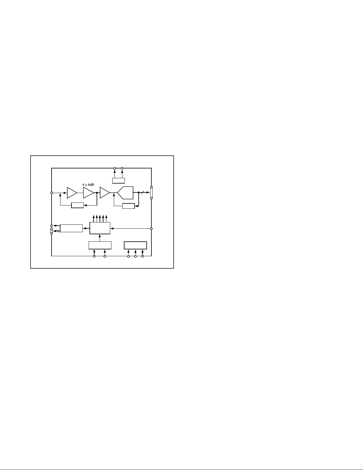
4. IC906 (CDS, AGC Circuit and A/D Converter)
The video signal which is output from the CCD is input to Pin
(27) of IC906. There are inside the sampling hold block, AGC
block and A/D converter block.
The setting of sampling phase and AGC amplifier is carried
out by serial data at Pin (32). The video signal is carried out
A/D converter, and is output by 10-bit.
5. Lens drive block
5-1. Shutter drive
The shutter drive signal (SIN1 and SIN2) which is output from
the ASIC expansion port (IC106) is drived the shutter constant
level driver (IC951), and then shutter plunger is opened and
closed.
5-2. Iris drive
The iris stepping motor drive signals (IIN1 and IIN2) which are
output from the ASIC (IC101) are used to drive by the motor
driver (IC951).
5-3. Focus drive
The focus stepping motor drive signals (FIN1, FIN2, FIN3 and
FIN4) which are output from the ASIC (IC101) are used to
drive by the motor driver (IC951). Detection of the standard
focusing positions is carried out by means of the
photointerruptor (FPI-E) inside the lens block.
CCDIN
RG
H1-H4
VRT
VREF
2~36 dB
VGA
PxGA
CDS
HORIZONTAL
4
DRIVERS
CLAMP
INTERNAL
CLOCKS
PRECISION
TIMING
CORE
SYNC
GENERATOR
VD
HD
Fig. 1-2. IC906 Block Diagram
VRB
ADC
CLAMP
REGISTERS
SL
INTERNAL
SCK
10
SDATA
DOUT
CLI
5-4. Zoom drive
The zoom DC motor drive signals (ZIN1 and ZIN2) which are
output from the ASIC (IC101) are used to drive by the motor
driver (IC951). Detection of the zoom positions is carried out
by means of photoreflector (ZPI-E) inside the lens block.
– 3 –
Page 3

6. Circuit description
6-1. Digital clamp
The optical black section of the CCD extracts averaged values from the subsequent data to make the black level of the
CCD output data uniform for each line. The optical black section of the CCD averaged value for each line is taken as the
sum of the value for the previous line multiplied by the coefficient k and the value for the current line multiplied by the
coefficient (k-1).
6-2. Signal processor
1. γ correction circuit
This circuit performs (gamma) correction in order to maintain
a linear relationship between the light input to the camera
and the light output from the picture screen.
2. Color generation circuit
This circuit converts the CCD data into RGB signals.
3. Matrix circuit
This circuit generates the Y signals, R-Y signals and B-Y signals from the RGB signals.
4. Horizontal and vertical aperture circuit
This circuit is used gemerate the aperture signal.
6-3. AE/AWB and AF computing circuit
The AE/AWB carries out computation based on a 256-segment screen, and the AF carries out computations based on
a 11-segment screen.
6-4. SDRAM controller
This circuit outputs address, RAS, CAS and AS data for controlling the SDRAM. It also refreshes the SDRAM.
6-5. Communication control
1. SIO
This is the interface for the 8-bit microprocessor.
7. Outline of Operation
When the shutter opens, the reset signals and the serial signals (“take a picture” commands) from the 8-bit microprocessor are input to ASIC (IC101) and operation starts. When the
TG/SG drives the CCD, picture data passes through the A/D
and CDS, and is then input to the ASIC as 12-bit data. The
AF, AE, AWB, shutter, and AGC value are computed from this
data, and three exposures are made to obtain the optimum
picture. The data which has already been stored in the SDRAM
is read by the CPU and color generation is carried out. Each
pixel is interpolated from the surrounding data as being either R, G and B primary color data to produce R, G and B
data. At this time, correction of the lens distortion which is a
characteristic of wide-angle lenses is carried out. After AWB
and γ processing are carried out, a matrix is generated and
aperture correction is carried out for the Y signal, and the
data is then compressed by the JPEG method by (JPEG) and
is then written to card memory (SD card).
When the data is to be output to an external device, it is taken
data from the memory and output via the USB. When played
back on the LCD and monitor, data is transferred from memery
to the SDRAM, and the data elongated by JPEG decorder is
displayed over the SDRAM display area.
8. LCD Block
LCD block is in the CP1 board, and it is constructed by VCOM
generation circuit etc.
The video signal from the ASIC are 6-bit digital signal, and
input to LCD directly. It is converted into RGB signals at driver
circuit in the LCD.
The VCOM (common polar voltage: AC) and the R, G and B
signals becomes greater, the display becomes darker; if the
difference in potential is smaller, the element opens and the
LCD become brighter. And also the timing pulse except the
video signal is input to LCD directly from ASIC.
2. PIO/PWM/SIO for LCD
8-bit parallel input and output makes it possible to switch between individual input/output and PWM input/output. It is prepared for 16-bit parallel output.
6-6. TG/SG
Timing generated for 3 million pixel CCD control.
6-7. Digital encorder
It generates chroma signal from color difference signal.
6-8. JPEG encorder and decorder
It is compressed and elongated the data by JPEG system.
– 4 –
Page 4

1-2. CP1 POWER CIRCUIT DESCRIPTION
1. Outline
This is the main power circuit, and is comprised of the following blocks.
Switching controller (IC501)
Analog system power output (T5001, Q5001, IC502)
Digital 3.25 V power output (L5004)
Digital 1.53 V power output (L5005)
5 V system power output (L5003, Q5009)
LCD 15 V system power output (L5001, Q5002)
Backlight power output (L5002)
Motor system power output (IC955, L9551, Q9551)
2. Switching Controller (IC501)
This is the basic circuit which is necessary for controlling the
power supply for a PWM-type switching regulator, and is provided with seven built-in channels, only CH2 (digital 3.25 V),
CH3 (digital 1.53 V), CH4 (digital system), CH5 (analog system), CH6 (LCD system) and CH7 (backlight sysetm) are used.
Feedback from 3.25 V (D) (CH2), 1.53 V (D) (CH3), digital
system (CH4), analog system (CH5), LCD system (CH6) and
backlight system (CH7) power supply outputs are received,
and the PWM duty is varied so that each one is maintained at
the correct voltage setting level.
Feedback for the backlight power (CH7) is provided to the
both ends voltage of registance so that regular current can
be controlled to be current that was setting.
4. Digital 3.25 V Power Output
+3.25 V (D) is output. Feedback for the +3.25 V (D) is provided to the switching controller (Pins (32) of IC501) so that
PWM control can be carried out.
5. Digital 1.53 V Power Output
+1.53 V (D) is output. Feedback for the +1.53 V (D) is provided to the swiching controller (Pin (31) of IC501) so that
PWM control can be carried out.
6. 5 V System Power Output
+5 V is output. Feedback for the +5 V is provided to the
swiching controller (Pin (52) of IC501) so that PWM control
can be carried out.
7. LCD System Power Output
+15 V (L) and 5 V (L) are output. Feedback for the +15 V (L) is
provided to the swiching controller (Pin (56) of IC501) so that
PWM control can be carried out.
8. Backlight Power Output
Regular current is being transmitted to LED for LCD backlight. Feedback for the both ends voltage of registance that is
being positioned to in series LED are provided to the switching controller (Pin (48) of IC501) so that PWM control to be
carried out.
2-1. Short-circuit Protection Circuit
If output is short-circuited for the length of time setting inside
(Pin (42) of IC501), all output is turned off. The control signal
(P ON) are recontrolled to restore output.
3. Analog System Power Output
+15.5 V (A), +3.45 V (A) and -8.0 V (A) are output. Feedback
for the +15.5 V (A) is provided to the switching controller (Pin
(53) of IC501) so that PWM control can be carried out. +3.45
V (A) is output which dropped 3.4 V by 5V system power output at regulator IC502.
9. Motor System Power Output
3.7 V is output. Feedback for the 3.7 V is provided to (Pin (1)
of IC955) so that PWM control can be carried out.
– 5 –
 Loading...