

Page 1
1. OUTLINE OF CIRCUIT DESCRIPTION
1-1. CA-A CIRCUIT DESCRIPTIONS
Around CCD block
1. IC Configuration
IC903 (RJ24J1AA0PT) CCD imager
IC902 (TC74VHC04FTP) H driver
IC904 (LR366854) V driver
IC905 (AD9806KST) CDS, AGC, A/D converter
PI4
PI3
(NC)
3 2 1 21
4
(NC)
(NC)
2324
(NC)
22
PI2
PI1
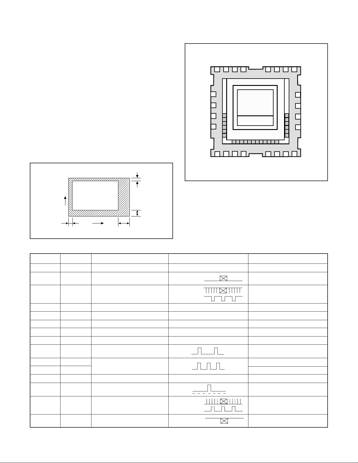
2. IC905 (CCD)
[Structure]
Frame transfer type CCD image sensor
Optical size 1/2.8 type
Effective pixels 1300 (H) x 980 (V)
Pixels in total 1353 (H) x 1006 (V)
Optical black
Horizontal (H) direction: left 2 pixels, right 51 pixels
Vertical (V) direction: upper 10 pixels, below 12 pixels
Dummy bit number Horizontal : 20 Vertical : 4
10
V
12
2
Fig. 1-1.Optical Black Location (Top View)
Pin No. Symbol
1, 2, 23, 24
NC
H
Pin Description
-
51
PS1
5
PS2
6
7
VPW
8
VOUT
9
Waveform
(LCC24
Top View)
10
11 12 16
PR
VSS
VDD
VRD
PH4
151413
PH1
Fig. 1-2. CCD Terminal Name
Voltage
PH2
20
19
18
17
PH3
PS3
PS4
NSUB
VOG
3, 4
5, 6
7
8
9
10
11
12
13, 15
14, 16
17
18
19, 20
PI3, PI4
PS1, PS2
PW
VOUT
VDD
VSS GND
VRD
PR
PH4, PH2
PH1, PH3
VOG
VSUB
PS4, PS3
21, 22 PI1, PI2
Image clock
Accumulation clock
P well
CCD output
Power
Reset drain
Reset gate
Horizontal register clock
CCD output gate
N substrate
Accumulation clock
Image clock
Table 1-1. CCD Pin Description
Frame shift
Frame shift
Line sending
Frame shift
Line sending
Frame shift
DC
DC
DC
DC
DC
DC
0~12 V
0~12 V
8 V
Approx. 13 V
20 V
0 V
20 V
L=18 V, H=23 V
L=2.5 V, H=7.5 V
L=0 V, H=5 V
3.3 V
L=26 V, H=29 V
0~12 V
0~12 V
– 2 –
Page 2
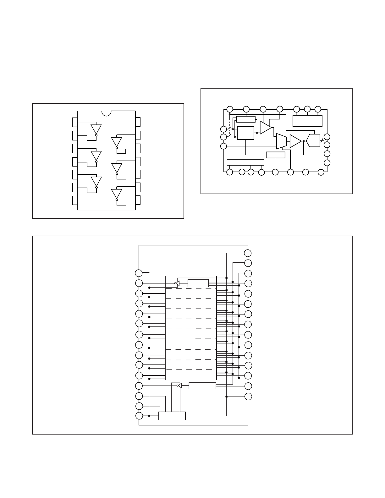
3. IC903 (H Driver) and IC902 (V Driver)
An H driver (IC903) and V driver (IC902) are necessary in
order to generate the clocks (vertical transfer clock, horizontal transfer clock and electronic shutter clock) which driver
the CCD.
IC902 is an inverter IC which drives the horizontal CCDs (H1
and H2). In addition the VREG 0~7, VXREG2 and VXREG3
signals which are output from IC102 are the vertical transfer
clocks. The clock is drived until peak value which necessary
CCD at IC902.
14
CC
1A
1Y
2A
2Y
3A
3Y
GND
1
2
3
4
5
6
7
V
13
6A
12
6Y
11
5A
10
5Y
4A
9
4Y
8
4. IC901 (CDS, AGC Circuit and A/D Converter)
The video signal which is output from the CCD is input to
Pins (26) and (27) of IC901. There are S/H blocks inside IC905
generated from the XSHP and XSHD pulses, and it is here
that CDS (correlated double sampling) is carried out.
After passing through the CDS circuit, the signal passes
through the AGC amplifier. It is A/C converted internally into
a 10-bit signal, and is then input to IC102.
SHD ADCCLK
22
21
GENERATOR
16
TIMING
A/D
AD9802
3341
ACVDD
ADVDD
43
10
2
DOUT
11
DRVDD
12
DVDD
17
PIN
DIN
ADCIN
PBLK
CLPDM SHP
CLAMP
27
26
CDS
29
2319
PGA
36
CLAMP
REFERENCE
48
37 20
CMLEVEL
VRT
47
VTB
STBY CLPOB
18
Fig. 1-5. IC901 Block Diagram
30
MUX S/H
ADCMODE
Fig. 1-3. IC903 Block Diagram
GND
1
OUT_1
2
OUT_2
3
OUT_3
4
OUT_4
5
OUT_5
6
OUT_6
7
OUT_7
8
OUT_8
9
OUT_9
10
OUT_10
OUT_NSUB
CAP5V
CAPNS
GND
11
12
13
14
15
Power circuit
OCNT circuit
DUTY circuit
OCNT circuit
30
29
28
27
26
25
24
23
22
21
20
19
18
17
16
VDD
OCNT
DUTY
IN_1
IN_2
IN_3
IN_4
IN_5
IN_6
IN_7
IN_8
IN_9
IN_10
IN_NSUB
VDD
Fig. 1-4. IC902 Block Diagram
– 3 –
Page 3

5. Transfer of Electric Charge by the Horizontal CCD
The transfer system for the horizontal CCD emplays a 4-phase drive method.
The electric charges sent to the final stage of the horizontal CCD are transferred to the floating diffusion (FD), as shown in Fig.
1-6. PR is turned on by the timing in (1), and the floating diffusion is charged to the potential of RD.
The PR is turned off by the timing in (2). In this condition, the floating diffusion is floated at high impedance.
The H2 potential becomes shallow by the timing in (3), and the electric charge now moves to the floating diffusion.
Here, the electric charges are converted into voltages at the rate of V = Q/C by the equivalent capacitance C of the floating
diffusion. PR is then turned on again by the timing in (1) when the H2 potential becomes deep.
Thus, the potential of the floating diffusion changes in proportion to the quantity of transferred electric charge, and becomes
CCD output after being received by the source follower. The equivalent circuit for the output circuit is shown in Fig. 1-7.
Reset gate pulse
Direction of transfer
(1)
(2)
(3)
PR
PR
PR
OG
H2
H1 H4 H3 H2 H1 H4 H3
(1)(2)
FDRD
H3
H4
OG
H2
H1 H4 H3 H2 H1 H4 H3
H1
FDRD
H2
PR
OG
H2
H1 H4 H3 H2 H1 H4 H3
FDRD
CCD OUT
(3)
Fig. 1-6. Horizontal Transfer of CCD Imager and Extraction of Signal Voltage
6. Lens drive block
6-1. Shutter drive
The regulator (IC952) drives by P ON signal which is output
20 V Pre-charge drain bias (PD)
from the power control IC (IC501) is drived, and then power is
supplied to iris shutter drive IC (IC951). The drive signal
(GPIO4, GPIO5, GPIO6, GPIO7) which is output from the
ASIC (IC102) is drived the iris shutter drive IC (IC951), and
the iris shutter spring is open and closed.
H Register
Electric
charge
Floating diffusion gate is
floated at a high impedance.
C is charged
equivalently
Voltage output
Fig. 1-7. Theory of Signal Extraction Operation
– 4 –
Page 4

1-2. CA-B CIRCUIT DESCRIPTION
1. Circuit description
1-1. PTG
This is program timing generator. Generates the timing signal
that is needed in order to drive the FT-CCD sensor.
1-2. FCP
The FCP receives the output data from the FT-CCD sensor
via the PTG, and then carries out various processing operations on the data (such as gamma correction and white
banance).
1-3. ITP
The ITP is a pixel conversion processor. It carries out various
processing operations (such as contour emphasis and chroma)
on the image data that is input from the FCP or from memory,
and then stores the processed data in memory.
1-4. CPU
This is 32 bit RISC CPU.
1-5. Memory controller
This is controlled SDRAM, flash ROM and CF card etc.
1-6. Video player
Outputs the RGB signals that are needed to control the graphic
overlay function and to drive the LCD.
1-7. GPIO
This is a multipurpose I/O. (It can be used as an input/output
port.)
1-8. COM port
This is communication block. Supports USB communication.
2. Outline of Operation
When the shutter opens, detect the 8-bit microprocessor and
transmit to record operation starts.
When the PTG drives the FT-CCD, picture data passes
through the A/D and is then input to the ASIC as 10-bit data.
This data then sends FCP, after which it is carried out various
processing operations on the data (such as gamma correction and white balance). The data is then sent to the ITP where
processing such as contour emphasis and chroma are carried out, after which it is temporarily stored in the SDRAM.
In case of still picture the data is then compressed by the
JPEG method and in case of picture it is compressed by
MJPEG method and is written to compact flash card.
3. LCD Block
RGB signals corresponding to the LCD driver are output from
the ASIC (video player). The LCD driver converts the RGB
signals that are output from the ASIC to a signal level that is
appropriate for the LCD monitor. These RGB signals and the
control signal which is output by the LCD driver are used to
drive the LCD panel.
The RGB signals are 1H transposed so that no DC component is present in the LCD element, and the two horizontal
shift register clocks drive the horizontal shift registers inside
the LCD panel so that the 1H transposed RGB signals are
applied to the LCD panel.
Because the LCD closes more as the difference in potential
between the VCOM (common polar voltage: fixed at DC) and
the R, G and B signals becomes greater, the display becomes
darker; if the difference in potential is smaller, the element
opens and the LCD become brighter. In addition, the brightness and contrast settings for the LCD can be varied by means
of the serial data from the ASIC.
1-9. Serial communication
This is the interface for the 8-bit microprocessor.
1-10. LCD driver
The RGB output signals that are output from the ASIC are
converted to a signal level that is appropriate for the LCD monitor.
1-11. LCD monitor
This is the image display device which displays the image
signals supplied from the LCD driver.
– 5 –
Page 5

1-3. CP1 POWER CIRCUIT DESCRIPTION
1. Outline
This is the main power circuit, and is comprised of the following blocks.
Switching controller (IC501)
Digital 5 V and analog system power output (T5001, Q5001)
Digital 2.5 V system power supply (Q5007)
Digital 3.4 V system power supply (Q5018)
LCD system power supply (Q5008, T5002)
Backlight power supply output (Q5013)
Inverter output (T5003, Q5017)
2. Switching Controller (IC501)
This is the basic circuit which is necessary for controlling the
power supply for a PWM-type switching regulator, and is provided with five built-in channels, only CH2 (digital 5 V, analog
system), CH4 (LCD system), CH3 (digital 2.5 V), CH1 (digital
3.4 V) and CH5 (backlight system) are used. Feedback from
5 V (D) (CH2), 2.5 V (D) (CH3) , 12.4 V (L) (CH4), 3.4 V (D)
(CH1) and 7 V (L) (CH5) power supply outputs are received,
and the PWM duty is varied so that each one is maintained at
the correct voltage setting level.
2-1. Short-circuit protection circuit
If output is short-circuited for the length of time determined
by the condenser which is connected to Pin (29) of IC501, all
output is turned off. The control signal (P ON) are recontrolled
to restore output.
3. Digital 3.4 V Power Output
3.4 V (D) is output. Feedback is sent to pin (41) of the switching controller (IC501) for PWM control to be carried out.
4. Digital 5 V and Analog System Power Output
5.1 V (D) , 26.4 V (A), 20 V (A), 13 V (A) and 5.1 V (A) are
output. Feedback for the 5.1 V (D) is provided to the switching controller (Pins (35) of IC501) so that PWM control can
be carried out.
5. Digital 2.5 V System Power Output
2.5 V (D) is output. Feedback is provided to the swiching controller (Pin (23) of IC501) so that PWM control can be carried
out.
6. LCD System Power Output
12.4 V (L) is output. Feedback for the 12.4 V (L) is provided
to the switching controller (Pins (22) of IC501) so that PWM
control can be carried out.
7. Backlight Power Supply output
7.0 V (L) is output. Feedback is sent to pin (17) of the switching controller (IC501) for PWM control to be carried out.
8. Inverter Output
The backlight uses a flat picture tube. When INV CLK is input, Q5017 carries out switching operations, so that T5003 is
energized and a high-voltage pulse is generated between pins
(3) and (4) of T5003. This high-voltage pulse is applied to the
backlight to make it illuminate.
– 6 –
 Loading...