

Page 1
SERVICE MANUAL
FILE NO.
Digital Camera
Contents
1. OUTLINE OF CIRCUIT DESCRIPTION .................... 2
2. DISASSEMBLY ........................................................ 10
3. ELECTRICAL ADJUSTMENT .................................. 12
4. USB STORAGE INFORMATION
REGISTRATION ...................................................... 17
5. TROUBLESHOOTING GUIDE................................. 18
6. PARTS LIST............................................................. 19
CABINET AND CHASSIS PARTS 1 ........................ 19
CABINET AND CHASSIS PARTS 2 ........................ 20
ELECTRICAL PARTS .............................................. 21
PACKING MATERIALS............................................ 26
ACCESSORIES ....................................................... 26
AC ADAPTOR .......................................................... 26
CIRCUIT DIAGRAMS &
PRINTED WIRING BOARDS ...................................... C1
VPC-MZ3EX
(Product Code : 126 612 01)
(Europe)
(PAL General)
VPC-MZ3
(Product Code : 126 612 02)
(U.S.A.)
(Canada)
VPC-MZ3GX
(Product Code : 126 612 03)
(General)
VAR-G6U
(Product Code : 126 301 09)
(U.S.A.)
(Canada)
VAR-G6EX
(Product Code : 126 301 10)
(Europe)
(PAL General)
VAR-G6E
(Product Code : 126 301 11)
(U.K.)
PRODUCT SAFETY NOTICE
The components designated by a symbol ( ! ) in this schematic diagram designates components whose value are of
special significance to product safety. Should any component designated by a symbol need to be replaced, use only the part
designated in the Parts List. Do not deviate from the resistance, wattage, and voltage ratings shown.
CAUTION : Danger of explosion if battery is incorrectly replaced.
Replace only with the same or equivalent type recommended by the manufacturer.
Discard used batteries according to the manufacturer’s instructions.
NOTE : 1. Parts order must contain model number, part number, and description.
2. Substitute parts may be supplied as the service parts.
3. N. S. P. : Not available as service parts.
Design and specification are subject to change without notice.
SX612/EX, U, GX, SVA03/U, EX, E
REFERENCE No. SM5310441
Page 2
1. OUTLINE OF CIRCUIT DESCRIPTION
1-1. CA1 and A PART OF CA2 CIRCUIT
DESCRIPTIONS
Around CCD block
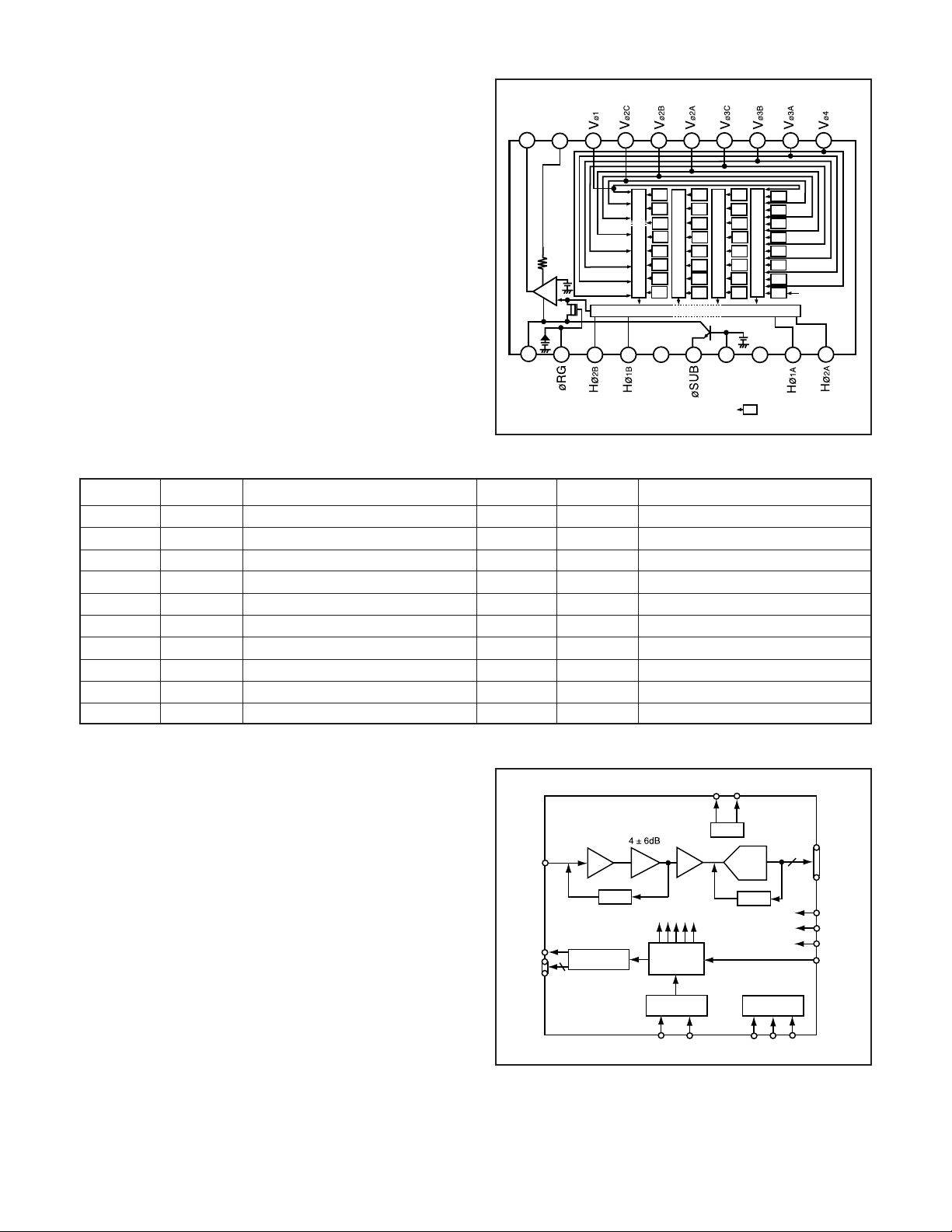
1. IC Configuration
CA1 board
IC901 (ICX274AQ) CCD imager
CA2 board
IC901 (H driver, CDS, AGC and A/D converter)
2. IC901 (CA1) (CCD imager)
[Structure]
Interline type CCD image sensor
Image size Diagonal 8.293 mm (1/1.8 type)
Pixels in total 1688 (H) x 1248 (V)
Recording pixels 1600 (H) x 1200 (V)
10
11
OUT
V
DD
V
GND
7
6
5
B
G
R
G
G
B
R
G
G
B
R
Vertical register
G
B
G
R
G
Horizontal register
15
16
GND
(Note) : Photo sensor
12
8
9
13
14
Fig. 1-1. CCD Block Diagram
17
3
4
G
R
G
R
G
R
G
R
18
L
V
SUB
C
1
2
B
G
B
G
B
G
B
G
(Note)
20
19
Pin No.
1
2
3
4
5
6
7
8
9
10
Symbol
4
Vø
Vø3A
Vø3B
Vø3C
Vø2A
Vø2B
Vø2C
Vø1
GND
V
OUT
Vertical register transfer clock
Vertical register transfer clock
Vertical register transfer clock
Vertical register transfer clock
Vertical register transfer clock
Vertical register transfer clock
Vertical register transfer clock
Vertical register transfer clock
GND
Signal output
Pin Description
Table 1-1. CCD Pin Description
3. IC904 (V Driver) and IC901 (CA2 board) (H driver)
An H driver and V driver are necessary in order to generate
the clocks (vertical transfer clock, horizontal transfer clock
and electronic shutter clock) which driver the CCD.
IC904 are V driver. In addition the XV1-XV4 signals which are
output from IC102 are the vertical transfer clocks, and the
XSG signal which is output from IC102 is superimposed onto
XV2 and XV3 at IC902 in order to generate a ternary pulse.
In addition, the XSUB signal which is output from IC102 is
used as the sweep pulse for the electronic shutter. A H driver
is inside IC901 (CA2 board), and H1A, H1B, H2A, H2B and
RG clock are generated at IC901 (CA2 board).
4. IC901 (CA2 board)
(CDS, AGC Circuit and A/D Converter)
The video signal which is output from the CCD is input to Pin
(29) of IC901 (CA2 board). There are inside the sampling hold
block, AGC block and A/D converter block.
The setting of sampling phase and AGC amplifier is carried
out by serial data at Pin (37) of IC911. The video signal is
carried out A/D converter, and is output by 10-bit.
Pin No.
11
12
13
14
15
16
17
18
19
20
CCDIN
RG
H1-H4
Symbol
V
DD
øRG
Hø
Hø1B
GND
øSUB
SUB
C
V
Hø1A
Hø2A
CDS
HORIZONTAL
4
DRIVERS
2B
L
CLAMP
Circuit power
Reset gate clock
Horizontal register transfer clock
Horizontal register transfer clock
GND
Substrate clock
Substrate bias
Protection transistor bias
Horizontal register transfer clock
Horizontal register transfer clock
PxGA
INTERNAL
PRECISION
GENERATOR
HD
2~36 dB
VGA
CLOCKS
TIMING
CORE
SYNC
VD
Pin Description
VRT
VREF
Fig. 1-2. IC901 Block Diagram
VRB
ADC
CLAMP
INTERNAL
REGISTERS
SL
SCK
12
SDATA
DOUT
CLPOB
CLPDM
PBLK
CLI
– 2 –
Page 3

1-2. CA2 CIRCUIT DESCRIPTION
1. Circuit Description
1-1. Scannning converter (Interlace converter)
This circuit uses the function of a 128-Mbit SDRAMs to convert the non-interlaced signal which is output from the CCD
into an interlaced signal for the video monitor.
1-2. Camera signal processor
This comprises circuits such as the digial clamp circuit, white
balance circuit, γ circuit, color signal generation circuit, matrix circuit and horizontal aperture circuit.
1. Digital clamp circuit
The optical black section of the CCD extracts 16-pixel averaged values from the subsequent data to make the black level
of the CCD output data uniform for each line. The 16-pixel
averaged value for each line is taken as the sum of the value
for the previous line multiplied by the coefficient k and the
value for the current line multiplied by the coefficient 1-k.
2. White balance circuit
This circuit controls the white balance by using the AWB judgement value computed by the CPU to control the gain for each
R, G and B pixel based on the CCD data which has been
read.
3. γ circuit
This circuit performs (gamma) correction in order to maintain
a linear relationship between the light input to the camera
and the light output from the picture screen.
4. Color generation circuit
This circuit converts the CCD data into RGB signals.
5. Matrix circuit
This circuit generates the Y signals, R-Y signals and B-Y signals from the RGB signals.
6. Horizontal aperture circuit
This circuit is used generate the aperture signal.
1-3. SDRAM controller
This circuit outputs address, RAS, CAS and AS data for controlling the SDRAM. It also refreshes the SDRAM.
1-4. PIO
The expansion parallel port can be used for functions such
as stroboscope control and LCD driver control.
1-8. Sound buffer
Audio memory
1-9. LCD driver
The 8-bit digital YUV signals which are input to the LCD driver
are converted to RGB signals, and the timing signal which is
necessary for LCD monitor display and the RGB signals are
then supplied to the LCD monitor.
1-10. LCD monitor
This is the image display device which displays the image
signals supplied from the LCD driver.
1-11. Memory card control
This reads data from the memory card and stores it in SDRAM,
and writes out the image data stored in SDRAM. In addition,
error correction is carried out when the data is read.
1-12. MJPEG compression
Still and continuous frame data is converted to JPEG format,
and movie images are compressed and expanded in MJPEG
format.
2. Outline of Operation
When the shutter opens, the reset signals, ZTEST0, ZTEST1,
ZTEST2 signals and the serial signals (“take a picture” commands) from the 8-bit microprocessor are input and record
operation starts. When the TG drives the CCD, picture data
passes through the A/D and is then input to the ASIC as 10bit data. This data then passes through the DCLP, AWB, shutter
and γ circuit, after which it is input to the SDRAM. The AWB,
shutter, γ, and AGC value are computed from this data, and
two exposures are made to obtain the optimum picture. The
data which has already been stored in the SDRAM is read by
the CPU and color generation is carried out. Each pixel is
interpolated from the surrounding data as being either R, G
or B primary color data to produce R, G and B data. At this
time, correction of the lens distortion which is a characteristic
of wide-angle lenses is carried out. Aperture correction is carried out, and in case of still picture the data is then compressed
by the JPEG method and in case of picture it is compressed
by MJPEG method and is written to compact flash card. When
the data is to be output to an external device, it is read JPEG
picture data from the compact flash card and output to PC via
the USB.
1-5. SIO (Serial control)
This is the interface for the 4-bit microprocessor.
1-6. USB control
This is comunicated PC with 12 Mbps.
1-7. TG, SG block
This is the timing generation circuit which generates the clocks
(vertical transfer clock and electronic shutter clock) which drive
the CCD.
– 3 –
Page 4

3. LCD Block
During EE, gamma conversion is carried out for the 10-bit
RGB data which is input from the A/D conversion block of the
CCD to the ASIC in order that the γ revised can be displayed
on the video. The YUV of 640 x 480 is then transferred to the
SVRAM.
The data which has accumulated in the SDRAM is converted
to digital YUV signal in conformity to ITUR-601 inside the ASIC
by SDRAM control circuit inside the ASIC, the data is sent to
the LCD driver IC and displayed the image to LCD panel.
If the shutter button is pressed in this condition, the 10-bit
data which is output from the A/D conversion block of the
CCD is sent to the SDRAM (DMA transfer), and is displayed
on the LCD as a freeze-frame image.
During playback, the JPEG image data which has accumulated in the compact flash card is converted to YUV signals.
In the same way as for EE, the data is then sent to the SDRAM,
converted to digital YUV signal in conformity to ITUR-601 inside the ASIC, the data is sent to the LCD driver IC and displayed the image to LCD panel.
The LCD driver is converted digital YUV signals to RGB signals from ASIC, and these RGB signals and the control signal which is output by the LCD driver are used to drive the
LCD panel. The RGB signals are 1H transposed so that no
DC component is present in the LCD element, and the two
horizontal shift register clocks drive the horizontal shift registers inside the LCD panel so that the 1H/1V transposed RGB
signals are applied to the LCD panel.
Because the LCD closes more as the difference in potential
between the VCOM (common polar voltage: AC drive) and
the R, G and B signals becomes greater, the display becomes
darker; if the difference in potential is smaller, the element
opens and the LCD become brighter. In addition, the brightness and contrast settings for the LCD can be varied by means
of the serial data from the ASIC.
– 4 –
Page 5

1-3. PW1 POWER CIRCUIT and LENS DRIVE
BLOCK DESCRIPTION
1. Outline
This is the main power circuit, and is comprised of the following blocks.
Switching power controller (IC501)
Analog and LCD system power output (Q5001, T5001)
Digital 1.85 V power output (Q5009, L5008)
Digital 3.35 V power output (Q5010, L5009)
Digital 3.35 V step-up power output (Q5011, L5010)
LED backlight power output (Q5012, L5011)
5 V system power output (Q5015, L5012)
2. Switching Controller
This is the basic circuit which is necessary for controlling the
power supply for a PWM-type switching regulator, and is provided with six built-in channels, only CH1 (analog and LCD
system power output), CH2 (digital 1.85 V system power output), CH3 (digital 3.35 V system power output), CH4 (digital
3.35 V step-up power output), CH5 (LED back light power
output) and CH6 (5 V system power output) are used. Feedback from 15.0 V (A) (CH1), 1.85 V (D) (CH2), 3.35 V (D)
(CH3), 4.7 V (L) (CH4), LED backlight output (CH5) and 5 V
(CH6) power supply outputs are received, and the PWM duty
is varied so that each one is maintained at the correct voltage
setting level.
2-1. Short-circuit Protection
If output is short-circuited for the length of time determined
by the condenser which is connected to Pin (37) of IC501, all
output is turned off. The control signal (P ON) are recontrolled
to restore output.
3. Analog and LCD System Power Output
15.0 V (A), -7.5 V (A) and 9.6 V (L) are output. Feedback for
the 15.0 V (A) is provided to the switching controller (Pin (40)
of IC501) so that PWM control can be carried out.
7. LED Backlight Power Output
A constant current flows to the backlight LEDs. Feedback for
the voltage of R5098 is provided to the power controller (Pin
(2) of IC501) so that PWM control can be carried out.
8. 5 V System Power Output
5 V is output. Feedback for the 5 V is provided to the swiching
controller (Pin (4) of IC501) so that PWM control can be carried out.
9. Lens drive block
9-1. Iris drive
When the drive signals (IRIS_A, IRIS_/A, IRIS_B and IRIS_/
B) which are output from the ASIC, the stepping motor is driven
by the driver (IC951), and are then used to drive the iris steps.
9-2. Focus drive
When the drive signals (FRSTB, FCW, FOEB and FCLK) which
are output from the ASIC, the focus stepping motor is sinewave driven by the micro-step motor driver (IC953). Detection
of the standard focusing positions is carried out by means of
the photointerruptor (FOCUS PI) inside the lens block.
9-3. Iris drive
The zoom DC motor drive signals (ZOOM_A and ZOOM_/A)
which are output from the ASIC are used to drive by the motor
driver (IC951). Detection of the zoom positions is carried out
by means of photointerruptor (ZOOM PI) inside the lens block.
9-4. Shutter drive
When the shutter drive signals (SHUT_A and SHUT_/A) which
are output from the ASIC, it is driven regular current by the
motor driver IC (IC951).
4. Digital 1.85 V Power Output
1.85 V (D) is output. Feedback for the 1.85 V (D) is provided
to the switching controller (Pins (43) of IC501) so that PWM
control can be carried out.
5. Digital 3.35 V Power Output
3.35 V (D) is output. Feedback for the 3.35 V (D) is provided
to the swiching controller (Pin (45) of IC501) so that PWM
control can be carried out.
6. Digital 3.35 V Step-up Power Output
4.7 V is output. Feedback for the 4.7 V is provided to the
swiching controller (Pin (47) of IC501) so that PWM control
can be carried out.
– 5 –
Page 6

1-4. ST1 STROBE CIRCUIT DESCRIPTION
1. Charging Circuit
When UNREG power is supplied to the charge circuit and the
CHG signal from SY1 board becomes High (3.3 V), the charging circuit starts operating and the main electorolytic capacitor is charged with high-voltage direct current.
However, when the CHG signal is Low (0 V), the charging
circuit does not operate.
1-1. Power switch
When the CHG signal switches to Hi, Q5407 turns ON and
the charging circuit starts operating.
1-2. Power supply filter
C5401 constitutes the power supply filter. They smooth out
ripples in the current which accompany the switching of the
oscillation transformer.
1-3. Oscillation circuit
This circuit generates an AC voltage (pulse) in order to increase the UNREG power supply voltage when drops in current occur. This circuit generates a drive pulse with a frequency
of approximately 50-100 kHz. Because self-excited light omission is used, the oscillation frequency changes according to
the drive conditions.
2. Light Emission Circuit
When RDY and TRIG signals are input from the ASIC expansion port, the stroboscope emits light.
2-1. Emission control circuit
When the RDY signal is input to the emission control circuit,
Q5409 switches on and preparation is made to let current
flow to the light emitting element. Moreover, when a STOP
signal is input, the stroboscope stops emitting light.
2-2. Trigger circuit
When a TRIG signal is input to the trigger circuit, D5405
switches on, a high-voltage pulse of several kilovolts is generated inside the trigger circuit, and this pulse is then applied
to the light emitting part.
2-3. Light emitting element
When the high-voltage pulse form the trigger circuit is applied to the light emitting part, currnet flows to the light emitting element and light is emitted.
Beware of electric shocks.
1-4. Oscillation transformer
The low-voltage alternating current which is generated by the
oscillation control circuit is converted to a high-voltage alternating current by the oscillation transformer.
1-5. Rectifier circuit
The high-voltage alternating current which is generated at
the secondary side of T5401 is rectified to produce a highvoltage direct current and is accumulated at electrolytic capacitor C5412.
1-6. Voltage monitoring circuit
This circuit is used to maintain the voltage accumulated at
C5412 at a constance level.
After the charging voltage is divided and converted to a lower
voltage by R5417, R5419 and R5420, it is output to the SY1
circuit board as the monitoring voltage VMONIT. When this
VMONIT voltage reaches a specified level at the SY1 circuit
board, the CHG signal is switched to Low and charging is
interrupted.
– 6 –
Page 7

1-5. SY1 CIRCUIT DESCRIPTION
1. Configuration and Functions
For the overall configuration of the SY1 circuit board, refer to the block diagram. The SY1 circuit board centers around a 8-bit
microprocessor (IC301), and controls camera system condition (mode).
The 8-bit microprocessor handles the following functions.
1. Operation key input, 2. Clock control and backup, 3. Power ON/OFF, 4. Storobe charge control, 5. Signal input and output for
zoom and lens control.
Pin
1~4
5
6
7
8
9
10
11
12
13
14
15
16
17
18
19
20
21
22
23
24 VDD
25 AVSS
26~29 SCAN IN 3~0
30
31 NOT USED
32
33
34
35
36
37
38
39
40
41
42
43
44
45
46
47
48
STBY_LED (GREEN)
Signal
SCAN OUT 0~3
P ON
PA O N
LCD ON
BL_ON
VSS
VDD
SELF_LED
STBY_LED (RED)
AVREF_ON
SI
SO
SCK
PRG SI
PRG SO
PRG SCK
NOT USED
NOT USED
CHG ON
INT_TMP
CHG VOL
BATTERY
AVREF
AVDD
RESET
XCOUT
XCIN
IC
XOUT
XIN
VSS
BAT OFF
SREQ
SCAN IN6
INTP3
NOT USED
BOOT
I/O
O
O
O
O
O
O
O
O
O
O
I/O
O
I/O
O
O
O
I/O
Outline
Key matrix output
Digital power ON/OFF control H : ON
Analog power ON/OFF control H : ON
LCD power ON/OFF control H : ON
LCD backlight ON/OFF
-
-
I
I
-
-
-
-
I
I
-
I
I
-
-
I
I
I
I
-
I
I
I
I
-
GND
VDD
Self-timer LED control L : ON
Stand-by LED (green) control L : ON
Stand-by LED (red) control L : ON
A/D converter standard voltage control L : ON
Receiving data (from ASIC)
Sending data (to ASIC)
Communication clock (to ASIC)
Flash memory write receiving data
Flash memory write sending data
Flash memory write communication clock
-
-
Flash charge control H : ON
VDD
Analog GND
Key scan input
Internal temperature detection input (analog input)
-
Storobe charge voltage detection (analog input)
Battery voltage detection (analog input)
Analog standard voltage input terminal
A/D converter analog power terminal
Reset input
Clock oscillation terminal (32.768 kHz)
Clock oscillation terminal
Flash memory writing voltage
Main clock oscillation terminal (4MHz)
Main clock oscillation terminal
GND
Battery OFF detection
Serial communication requirement (from ASIC)
Key scan input 6
-
-
Compulsion boot control
See next page →
– 7 –
Page 8
49 AV JACK
50
51
52
53
54
55
56
57
58
59
60
61
62
63
64
DC IN
CARD
BUZZER
SCAN OUT 4
SCAN IN 4
SCAN IN 5
SUB1
USB
LCD ON2 O
NTZPAL O NTSC/PAL switch H : NTSC
BACKUP_CNT
ASIC TEST 0
ASIC TEST 1
ASIC TEST 2
ASIC RESET
I
O DC jack/battery detection input (analog input) L : DC jack insertion
I
O
I
O
I
I/O
I
O
O ASIC reset control signal 0
O ASIC reset control signal 1
O
O
Table 5-1. 8-bit Microprocessor Port Specification
AV jack connection detection H : AV jack detection
CF card insertion detection L : Insertion
Buzzer beep tone output H : Pulse output
Key scan output 4
Key scan input 4
Key scan input 5
Communication line to main
USB connector detection L : USB detecion
LCD ON/OFF control 2 H : ON
Backup battery charge control L : Charge ON
ASIC reset control signal 2
ASIC reset singal
2. Internal Communication Bus
The SY1 circuit board carries out overall control of camera operation by detecting the input from the keyboard and the condition
of the camera circuits. The 8-bit microprocessor reads the signals from each sensor element as input data and outputs this data
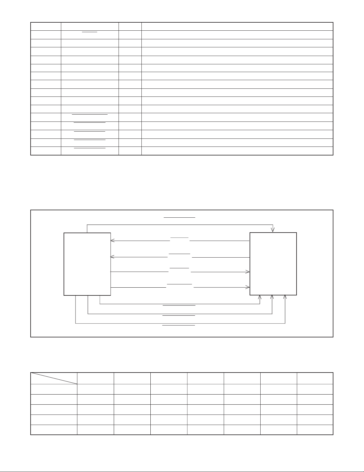
to the camera circuits (ASIC) or to the LCD display device as operation mode setting data. Fig. 5-1 shows the internal communication between the 8-bit microprocessor, ASIC and SPARC lite circuits.
ASIC RESET
S. REQ
8-bit
Microprocessor
Fig. 5-1 Internal Bus Communication System
ASIC SO
ASIC SI
ASIC SCK
ASIC TEST 1
ASIC TEST 2
ASIC TEST 0
3. Key Operaiton
For details of the key operation, refer to the instruction manual.
SCAN
OUT
SCAN
IN
0
1
2
3
0
← LEFT
PLAY
-
WEB
-
1
↑ UP
VF
-
DC MODE
-4
2
↓ DOWN
LCD
TEST
SET UP
-
3
→ RIGHT
WIDE
FOCUS
VIDEO CLIP
SHOOTING
-
4
MENU
TELE
FLASH
SEQUENTIAL
SHOT
-
ASIC
5
SET
-
1st
STILL IMAGE
-
6
-
-
2nd
-
POWER ON
Table 5-2. Key Operation
– 8 –
Page 9
4. Power Supply Control
The 8-bit microprocessor controls the power supply for the overall system.
The following is a description of how the power supply is turned on and off. When the battery is attached, a regulated 3.2 V
voltage is normally input to the 8-bit microprocessor (IC301) by IC302, so that clock counting and key scanning is carried out
even when the power switch is turned off, so that the camera can start up again. When the battery is removed, the 8-bit microprocessor operates in sleep mode using the backup capacitor. At this time, the 8-bit microprocessor only carries out clock
counting, and waits in standby for the battery to be attached again. When a switch is operated, the 8-bit microprocessor supplies
power to the system as required.
The 8-bit microprocessor first sets both the P (A) ON signal at pin (6) and the P ON signal at pin (5) to high, and then turns on the
DC/DC converter. After this, low signals are output from pins (61), (62), (63) and (64) so that the ASIC is set to the reset condition.
After this these pins set to high, and set to active condition. If the LCD monitor is on, the LCD ON 2 signal at pin (58) set to high,
and the DC/DC converter for the LCD monitor is turned on. Once it is completed, the ASIC returns to the reset condition, all DC/
DC converters are turned off and the power supply to the whole system is halted.
ASIC,
memory
Power voltage
Power OFF
Power switch ON-
Auto power OFF
Shutter switch ON
CAMERA
Monitor OFF
LCD finder
Play back
Table 5-3. Camera Mode (Battery Operation)
Note) 4 MHz = Main clock operation, 32 kHz = Sub clock operation
3.3 V 1.8 V
OFF
OFF
ON
OFF
ON
ON
CCD
5 V (A)
+12 V etc.
OFF
OFF
ON → 2 OFF
OFF
ON
OFF
(ALWAYS)
5. 8-bit D/A circuit (Audio)
This circuit converts the audio signals (analog signals) from the microphone to 8-bit digital signals.
8 bit
CPU
3.2 V
32KHz OFF
4 MHz OFF
4 MHz OFF
4 MHz OFF
4 MHz ON
4 MHz ON
LCD
MONITOR
5 V (L)
+8.5 V etc.
6. 8-bit A/D circuit (Audio)
The audio signals which were converted to digial form by the 8-bit A/D circuit are temporarily to a sound buffer and then recorded
in the SSFDC card. During playback, the 8-bit D/A circuit converts these signals into analog audio signals.
– 9 –
Page 10
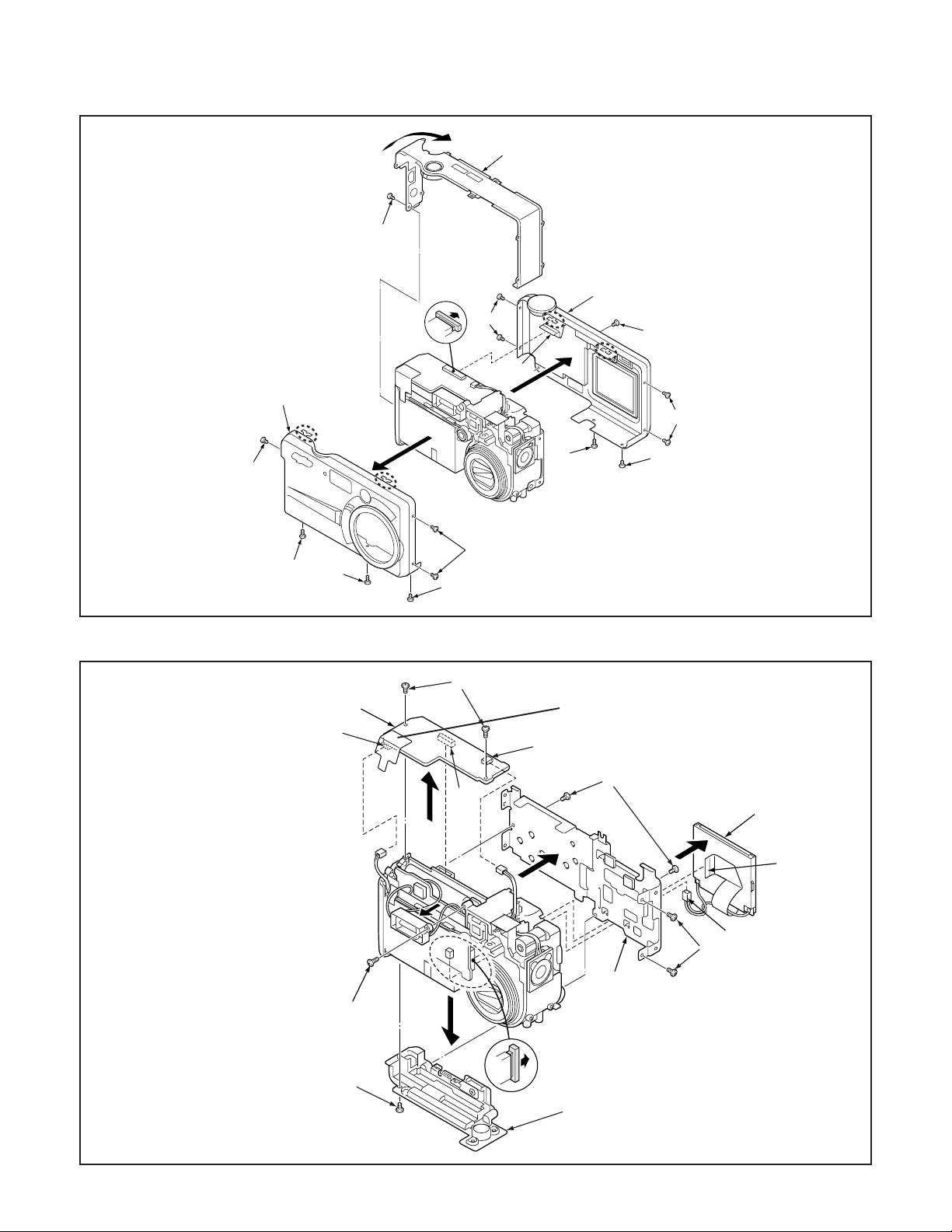
2. DISASSEMBLY
5
1
2
3
2
4
5
6
7
8
9
10
11
12
2-1. REMOVAL OF CABINET FRONT, CABINET BACK AND CABINET TOP
8
1. Six screws 1.7 x 2.5
2. Three screws 1.7 x 4
3. Four screws 1.7 x 2
4. Cabinet front
5. Cabinet back
6. FPC
7. Screw 1.7 x 2.5
8. Cabinet top
7
5
3
6
1
4
2
1
3
1
NOTE: Do not touch the holder cabi lock.
1
2
2
1
Because they change the shape
and get injured.
2-2. REMOVAL OF SY1 BOARD AND LCD
1. Two screws 1.7 x 3
2. Two connector
3. Connector
4. SY1 board
5. Four screws 1.7 x 3
6. Screw 1.7 x 3
7. Holder card
8. Holder monitor
9. FPC
10. Connector
11. LCD
12. Screw 1.7 x 4
NOTE: Attach the button buttery + side is
the bottom (Z3001 of SY1 board).
– 10 –
Page 11
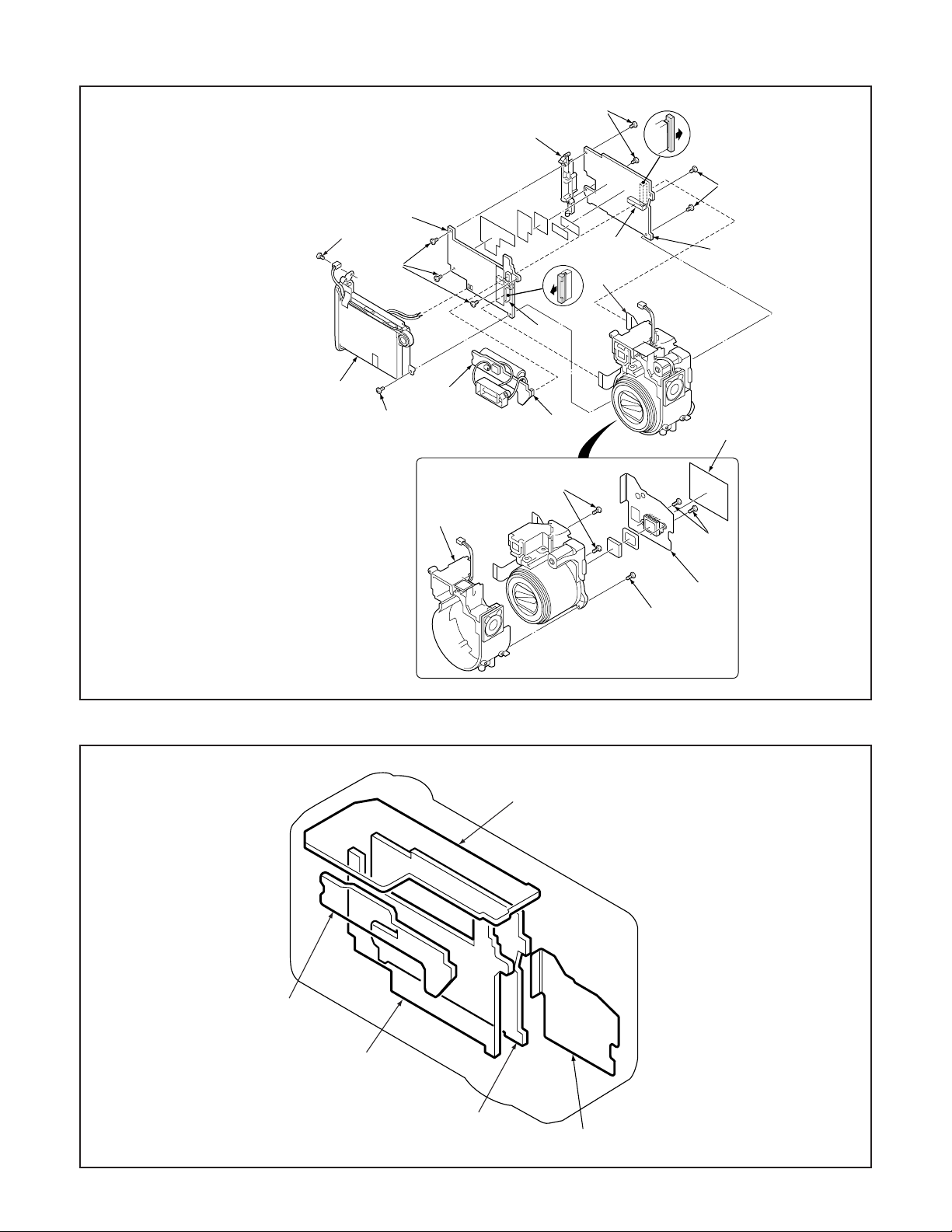
2-3. REMOVAL OF PW1 BOARD, CA2 BOARD, ST1 BOARD AND CA1 BOARD
11
1. FPC
2. Screw 1.7 x 3
3. Screw 1.7 x 4
4. Holder battery
5. Connector
6. ST1 board
7. Three screws 1.7 x 3
8. FPC
9. Connector
10. PW1 board
11. Four screws 1.7 x 3
12. Holder terminal
13. CA2 board
14. Spacer CA1
15. Two screws 1.4 x 3.5
16. CA1 board
17. Three screws 1.7 x 4
18. Holder lens
10
2
7
4
3
6
12
9
1
8
5
17
11
13
14
2-4. BOARD LOCATION
18
15
16
17
SY1 board
ST1 board
PW1 board
CA2 board
CA1 board
– 11 –
Page 12
3. ELECTRICAL ADJUSTMENT
Firmware
Image
AWB
Focus
UV Matrix
RGB Odd
RGB Gain
Tint
RGB Even
VCOMDC
Phase
LCD
Calibration
Upload
Initialize
LCD Type
H AFC Test
VCOMPP(LOW)
VCOMPP(HI)
Cal Data
Cal Mode
OK
OK
EVF
USB storage
Get
Set
VID
Set
PID
Set
Serial
Set
Rev.
Set
Setting
Language
Video Mode
VCO
3-1. Table for Servicing Tools
1
1
1
1Chroma meter
1
Part code
VJ8-0190
VJ8-0193
VJ8-0192
VJ8-0191
Ref. No.
J-1
J-2
J-3
Name
Pattern box (color viewer)
Siemens star chart
Calibration software
Number
J-4
J-5
Spare lump
Note: J-1 Pattern box (color viewer) is 100 - 110 VAC only.
J-1 J-2
J-3
J-4
Note: If the lens, CCD and board in item 2-6, it is necessary
to adjust again. Item 2-6 adjustments other than these
should be carried out in sequence. For 5 and 6, carry
out adjustment after sufficient charging has taken place.
In case of carrying out adjustment item 3 and 4 after
adjusting item 5 and 6, adjust item 3 and 4 after turing
off the power.
3-4. Setup
1. System requirements
Windows 98 or Me or 2000 or XP
IBM R -compatible PC with pentium processor
CD-ROM drive
3.5-inch high-density diskette drive
USB port
40 MB RAM
Hard disk drive with at least 15 MB available
VGA or SVGA monitor with at least 256-color display
2. Installing calibration software
1. Insert the calibration software installation diskette into your
diskette drive.
2. Open the explorer.
3. Copy the DscCalDI_129 folder on the floppy disk in the FD
drive to a folder on the hard disk.
J-5
3-2. Equipment
1. Oscilloscope
2. Digital voltmeter
3. AC adaptor
4. PC (IBM R -compatible PC, Pentium processor, Window
98 or Me or 2000 or XP)
3-3. Adjustment Items and Order
1. IC501 Oscillation Frequency Adjustment
2. CCD VSUB Adjustment
3. AWB Adjustment
4. Lens Adjustment
5. CCD Defect Detect Adjustment
6. CCD Black Point Defect Detect Adjustment
7. LCD Panel Adjustment
7-1. LCD RGB Offset Adjustment
7-2. LCD Gain Adjustment
3. Installing USB driver
Install the USB driver with camera or connection kit for PC.
4. Pattern box (color viewer)
Turn on the switch and wait for 30 minutes for aging to take
place before using Color Pure. It is used after adjusting the
chroma meter (VJ8-0192) adjust color temperature to 3100 ±
20 K and luminosity to 900 ± 20 cd/m
2
. Be careful of handling
the lump and its circumference are high temperature during
use and after power off for a while.
5. Computer screen during adjustment
– 12 –
Page 13
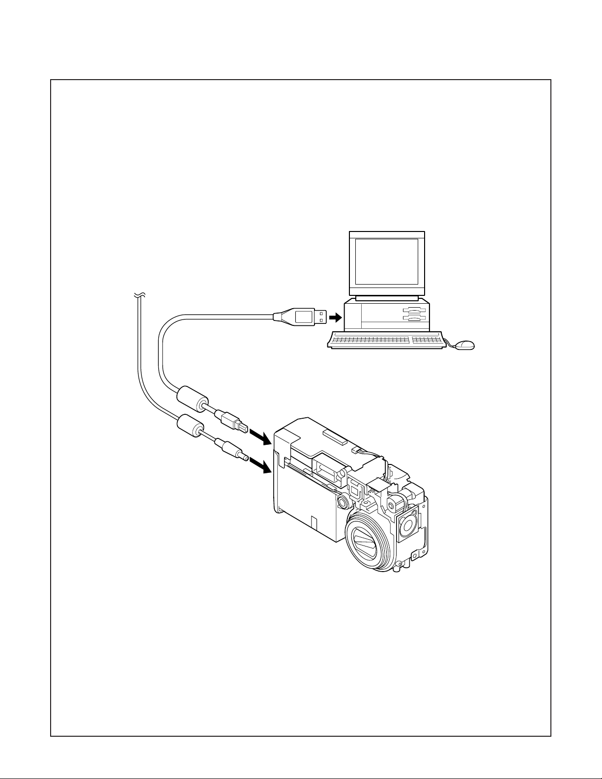
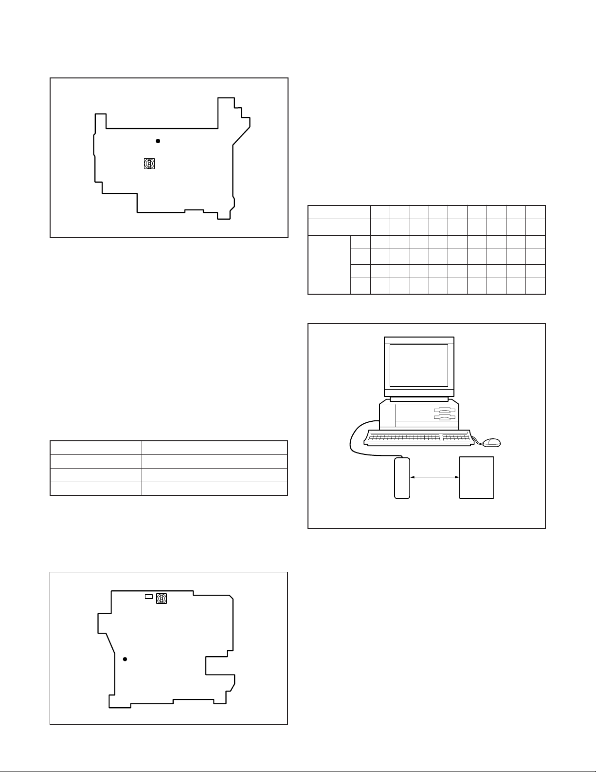
3-5. Connecting the camera to the computer
1. Line up the arrow on the cable connector with the notch on the camera's USB port. Insert the connector.
2. Locate a USB port on your computer.
To USB port
AC adaptor
USB cable
– 13 –
Page 14
3-6. Adjust Specifications
[PW1 board (Side B)]
CL526
VR501
Note:
1. When installing a new CCD, read the abbreviation described
on the rear side of CCD, and write it to the board.
2. If the CCD, each board and parts replaces, it is necessary
to adjust again.
Adjustment method:
1. Turn on the power. (Insert the DC jack.)
2. Shorten TP301 and TP302 of SY1 board with pushing S3003
(Flash sw).
3. Read the abbreviation display on the rear side of CCD.
Convert these to voltages using the table below.
For example, “h” → VSUB = 11.7 V
4. Adjust with VR921 so that the voltage of TP901 at VSUB
becomes the displayed voltage value ± 0.1 V.
Note:
1. Frequency adjustment is necessary to repair in the PW1
board and replace the parts. It is carried out with LCD
through screen display mode.
Preparation:
1. Carry out the frequency adjustment disconnecting cabinet
front, cabinet back, cabinet top and screws of holder battery. Side B of PW1 board can be seen.
2. Connect FPC of cabinet back to CN303.
3. Insert the compact flash.
4. Set the main switch to the camera mode.
5. Set the selector dial to the still image shooting mode.
6. Push the power switch, and comfirm that the through screen
from the CCD can be seen on the LCD.
1. IC501 Oscillation Frequency Adjustment
Measuring Point
Measuring Equipment
ADJ. Location
ADJ. Value
Adjustment method:
1. Adjust with VR501 to 496 ± 1 kHz.
CL526
Frequency counter
VR501
496 ± 1 kHz
VSUB abbreviation
Voltage
C
10.7
N
12.7
1
8.9
D
10.9E11.1
P
12.9
3. AWB Adjustment
Camera
2
9.139.349.5
f
11.5
11.3
R
S
13.5
13.3
13.1
0~18 cm
6
9.779.9810.1
G
H
11.7
U
V
13.7
Pattern box
(color viewer)
J
11.9
W
13.9
K
12.1
X
14.1
9
10.3
L
12.3
Y
14.3
A
10.5
m
12.5
Z
14.5
2. CCD VSUB Adjustment
[CA2 board (Side A)]
TP901
CL136(G)
VR501
Preparation:
POWER switch: ON
Adjusting method:
1. When setting the camera in place, set it to an angle so that
nothing appears in any part of the color viewer except the
white section. (Do not enter any light.)
2. Double-click on the DscCalDi129.
3. Click the AWB, and click the Yes.
4. AWB adjustment value will appear on the screen.
5. Click the OK.
– 14 –
Page 15
4. Lens Adjustment
6. CCD Black Point Defect Detect Adjustment
Camera
Siemens
star chart
Preparation:
POWER switch: ON
Adjustment condition:
More than A3 size siemens star chart
Fluorescent light illumination with no flicker
Illumination above the subject should be 400 lux ± 10 %.
Adjustment method:
1. Set the siemens star chart 100 cm ± 3 cm so that it becomes center of the screen.
2. Double-click on the DscCalDi129.
3. Click the Focus, and click the Yes.
4. Lens adjustment value will appear on the screen.
5. Click the OK.
5. CCD Defect Detect Adjustment
Preparation:
POWER switch: ON (Set the camera mode.)
Adjustment method:
1. Double-click on the DscCalDi129.
2. Select “CCD Defect” on the LCD “Test”, and click the “Ye s ”.
3. After the adjustment is completed, OK will display.
4. Click the OK.
Camera
0~18 cm
Pattern box
(color viewer)
Preparation:
POWER switch: ON
Adjusting method:
1. When setting the camera in place, set it to an angle so that
nothing appears in any part of the color viewer except the
white section. (Do not enter any light.)
2. Double-click on the DscCalDi129.
3. Select “CCD Black” on the LCD “Test”, and click the “Ye s ”.
4. After the adjustment is completed, the number of defect will
appear.
7. LCD Panel Adjustment
[CA2 board (Side A)]
TP901
VR501
CL136(G)
7-1. LCD RGB Offset Adjustment
Preparation:
POWER switch: ON
Adjusting method:
1. Double-click on the DscCalDi129.
2. Adjust LCD “RGB Odd” so that the amplitude of the CL136
waveform is 0.95 V ± 0.05 V.
3. Adjust LCD “RGB Even” so that the amplitude of the CL136
waveform is 4.55 V ± 0.05 V.
– 15 –
Page 16

4.55 ±
0.05 V
0.95 ± 0.05 V
CL136 waveform
7-2. LCD Gain Adjustment
Adjusting method:
1. Adjust LCD “RGB Gain” so that the amplitude of the CL136
waveform is 1.55 V ± 0.1 Vp-p.
Note:
7-1. LCD RGB Offset adjustment should always be carried
out first.
1.55 V
± 0.1 Vp-p
CL136 waveform
– 16 –
Page 17

4. USB STORAGE INFORMATION
REGISTRATION
USB storage data is important for when the camera is connected to a computer via a USB connection.
If there are any errors in the USB storage data, or if it has not
been saved, the USB specification conditions will not be satisfied, so always check and save the USB storage data.
Preparation:
POWER switch: ON
Adjustment method:
1. Connect the camera to a computer. (Refer to 3-5. Connecting the camera to the computer on the page 13.)
2. Double-click on the DscCalDi129.
3. Click on the Get button in the USB storage window and
check the USB storage data.
VID: SANYO
PID: VPC-MZ3 or VPC-MZ3EX
Serial:
Rev. : 1.00
4. Check the “Serial” in the above USB storage data. If the
displayed value is different from the serial number printed
on the base of the camera, enter the number on the base
of the camera. Then click the Set button.
5. Next, check VID, PID and Rev. entries in the USB storage
data. If any of them are different from the values in 3. above,
make the changes and then click the corresponding Set
button.
Calibration
AWB
Focus
UV Matrix
Cal Mode
Cal Data
USB storage
VID
Get
PID
Set
OK
OK
Upload
Firmware
Image
Initialize
EVF
LCD Type
LCD
RGB Odd
RGB Gain
Tint
VCO
H AFC Test
Serial
Set
Set
Rev.
RGB Even
VCOMDC
Phase
Set
Set
VCOMPP(LOW)
VCOMPP(HI)
Setting
Language
Video Mode
– 17 –
Page 18

5. TROUBLESHOOTING GUIDE
POWER LOSS INOPERTIVE
PUSH MAIN SW
IC301-45 (SCAN IN 6)
PULSE INPUT
YES
IC302-7 4.7 V
(BOOST 4.7 V)
HIGH
IC301-10
(VDD)
HIGH
IC301-36
(RESET)
HIGH
IC301-43
(BAT OFF)
HIGH
IC301-40
OSCILLATION
YES
IC301-37
OSCILLATION
YES
NO
CHECK CN303-3
LOW
CHECK PW1, IC952
LOW
LOW
CHECK IC302, R3004
LOW
NO
NO
CHECK R3003
CHECK X3001
CHECK X3002
CHECK IC302
TAKING INOPERATIVE
PUSH SHUTTER
BUTTON
IC301-55, 45
(SCAN IN 5, 6)
PULSE INPUT
YES
CN301-18, 15
(P ON, P(A) ON)
HIGH
SERIAL
COMMUNICATION
OK
CHECK CA2
NO
LOW
NG
CHECK S3001,
D3012, D3013,
R3038, R3037
CHECK IC301,
RB302, PW1
CHECK
IC301, CA2
CHECK IC301
NO PICTURE
CHECK CLK
OSCILLATION X1101,
IC111, R1101
YES
SD CLK
OSCILLATION
R1103
OK
IC102-62, 63
IC301-15, 16
OK
CHECK SOLDERING
OF MEMORY PIN
MAIN CLOCK FOR SYSTEM OPERATION
NO
NO OPERATION IF ABSENT
CHECK X1101 OSCILLATOR, R1101 AND IC111
SD RAM (IC103) MOVEMENT CLOCK
NG
NO READ PROGRAM FROM IC121 IF ABSENT
CHECK IC102, IC103
INCORRECT HAND
NG
SHAKING 8-BIT CPU
CHECK EACH INTERFACE
– 18 –
Page 19

6. PARTS LIST
LOCATION PARTS NO. DESCRIPTION LOCATION PARTS NO. DESCRIPTION
CABINET & CHASSIS PARTS 1
1 636 066 8195 RING-SX612/J
2 636 066 8867 ASSY,CABI FRONT-SX612/J
3 636 066 6993 BADGE SANYO-SX612/J
4 636 066 7174 SHAFT CARD-SX612/J
5 636 066 7044 COVER CARD-SX612/J
6 636 067 8095 SPRING COVER CF-SX612/J
7 636 066 7129 HOLDER CARD-SX612/J
8 636 066 7143 KNOB CARD-SX612/J
9 636 066 7181 SLIDE CARD-SX612/J
10 636 067 8088 SPRING SLIDE CF-SX612/J
11 645 056 6448 PAD(L=5)
12 636 066 5361 HOLDER MONITOR-SX612/J
13 636 067 8026 SPACER HOL MONITOR-SX612
14 636 067 8071 SPACER CV MONITOR B-SX612
15 636 067 8019 SPACER CV MONITOR A-SX612
16 636 067 7333 ASSY,WIRE LCD SX612 (N.S.P.)
17 645 054 8864 LCD(AL127ALXD0)
18 636 066 5477 SPACER MONTOR-SX612/J
19 645 054 4071 UNIT,CONTROL PANEL-SX612
20 636 067 7968 ADHESIVE TAPE UNIT B-612
21 636 067 7951 ADHESIVE TAPE UNIT A-612
22 636 066 5354 DEC CARD ACCESS-SX612/J
23 636 066 5279 ASSY,CABINET BACK-SX612/J
24 636 068 1927 SPACER CABI BACK-SX612/J
25 636 066 5347 DEC MONITOR-SX612/J
26 636 066 5439 REFLECTOR VF-SX612/J
27 636 066 5330 COVER EYE-SX612/J
28 636 066 8898 ASSY,CABI TOP-SX612/J
29 636 066 7082 HOLDER STRAP-SX612/J
30 411 000 9403 RING E 2
101 412 065 1203 SPECIAL SCREW-1.7X2.5
102 412 065 1104 SPECIAAL SCREW-1.7X4
103 412 065 3405 SPECIAL SCREW-1.4X1.7
104 412 063 6101 SPECIAL SCREW-1.7X3.0
105 412 065 1401 SPECIAL SCREW-1.4X2.5
106 411 177 8407 SCR S-TPG PAN PCS 1.7X3
107 412 065 4006 SPECIAL SCREW-1.4X2
108 412 065 1302 SPECIAL SCREW-1.7X2
N.S.P.: Not available as service parts.
29
101
101
30
28
19
12
21
108
107
20
106
23
11
20
18
22
13
102
24
14
106
101
15
25
106
26
27
101
108
17
16
3
2
102
SX612/J Parts List-1
9
103
10
105
101
104
6
102
1
101
4
5
8
7
19
Page 20

LOCATION PARTS NO. DESCRIPTION LOCATION PARTS NO. DESCRIPTION
CABINET & CHASSIS PARTS 2
31 636 066 9079 COMPL,REFLECTOR-SX612
32 636 068 0265 COVER TRIGER-SX612/J
33 636 066 4616 COMPL PWB,ST-1
34 636 066 5415 HOLDER LENS-SX612/J
35 636 066 5460 SPACER SPEAKER BACK-612/J
36 636 066 5446 SPACER SPEAKER BACK2-612J
37 645 055 1802 SPEAKER,8
38 636 066 5453 SPACER SPEAKER FRONT-612J
39 636 067 8057 SPACER HOLDER LENS-SX612
40 645 055 2243 LENS(ASSY),SZA4318
41 645 054 9960 OPTICAL FILTER
42 636 066 9505 SPACER
43 636 068 9848 COMPL,CA-1 SV-SX612
44 636 067 8033 SPACER CA1-SX612/J
45 636 067 8040 SPACER HOLDER BATT-SX612
46 636 064 8753 HOLDER MIC-SX212/J
47 645 055 1819 MICROPHONE
48 636 066 7099 HOLDER BATT F-SX612/J
49 636 066 8065 SPRING BATT EJECT-SX612/J
50 636 066 7105 HOLDER BATT B-SX612/J
51 636 066 7211 TERMINAL BATTERY A-612/J
52 636 066 7198 SPRING LEVER BATT-SX612/J
53 636 066 8577 LABEL CAUTION BATT-SX612
54 636 066 7150 LEVER BATT LOCK-SX612/J
55 636 066 7037 COVER BATT-SX612/J
56 636 066 7075 HOLDER P COVER-SX612/J
57 636 066 7167 SHAFT BATT-SX612/J
58 636 066 4609 COMPL PWB,PW-1
59 636 066 7136 HOLDER TERMINAL-SX612/J
60 636 066 4579 COMPL PWB,CA-2
61 636 067 8064 SPACER BACKUP-SX612/J
62 636 066 4593 COMPL PWB,SY-1
106 411 177 8407 SCR S-TPG PAN PCS 1.7X3
109 636 068 9848 COMPL PWB,CA-1 SV-SX612
110 411 181 8707 SCR S-TPG PAN PCS 1.4X3.5
N.S.P.: Not available as service parts.
106
61
62
106
55
46
56
47
57
106
45
32
33
54
53
106
48
106
52
49
58
109
59
50
106
51
39
40
60
109
106
106
44
43
110
110
42
41
109
SX612/J Parts List-2
109
31
34
35
36
37
38
20
Page 21

ELECTRICAL PARTS
Note:
1. Materials of Capacitors and Resistors are abbreviated as follows ;
Resistors Capacitors
MT-FILM Metallized Film Resistor MT-POLYEST Metallized Polyester Capacitor
MT-GLAZE Metallized Glaze Resistor MT-COMPO Metallized Composite Capacitor
OXIDE-MT Oxide Metallized Film Resistor TA-SOLD Tantalum Solid Capacitor
2. Tolerance of Capacitor (10pF over) and Resistor are noted with follow symboles.
F ............1% G ............2% J ............5% K ............10%
M ..........20% N ..........30% Z ..........+80% ~ -20%
3. Capacitors
µ
FP : pF
U :
4. Inductors
µ
H MH : mH
UH :
5. N.S.P. : Not available as service parts.
LOCATION PARTS NO. DESCRIPTION LOCATION PARTS NO. DESCRIPTION
COMPL,CA-1 SV-SX612
636 068 9848
C9001 403 157 1904 CERAMIC 10P D 50V
C9002 403 314 5905 CERAMIC 0.47U K 16V
C9003 403 314 5905 CERAMIC 0.47U K 16V
C9004 403 314 5905 CERAMIC 0.47U K 16V
C9005 403 314 5905 CERAMIC 0.47U K 16V
C9014 403 338 4403 CERAMIC 0.1U K 16V
C9016 403 283 6309 CERAMIC 1U Z 10V
C9017 403 333 3708 CERAMIC 10U M 10V
C9019 403 338 4403 CERAMIC 0.1U K 16V
C9020 403 332 8209 CERAMIC 10U M 16V
C9021 403 332 8209 CERAMIC 10U M 16V
C9022 403 320 5500 CERAMIC 1U Z 25V
Q9002 405 153 6709 TR 2SC3931-D
R9015 401 105 7503 MT-GLAZE 82K JA 1/16W
R9020 401 105 0405 MT-GLAZE 100 JA 1/16W
R9021 401 105 4106 MT-GALZE 3.3K JA 1/16W
R9022 401 105 7909 MT-GLAZE 0.000 ZA 1/16W
409 529 5907 IC ICX274AQF-C (N.S.P.)
636 066 5422 MOUNTING,LENS (N.S.P.)
(CAPACITORS)
(SEMICONDUCTOR)
(RESISTORS)
(MISCELLANEOUS)
COMPL PWB,CA-2
636 066 4579
C1001 403 345 3802 TA-SOLID 22U M 4V
C1002 403 346 2309 CERAMIC 0.1U K 10V
C1004 403 346 2309 CERAMIC 0.1U K 10V
C1005 403 346 2309 CERAMIC 0.1U K 10V
C1006 403 345 3802 TA-SOLID 22U M 4V
C1007 403 343 3101 CERAMIC 1U K 6.3V
C1008 403 346 2309 CERAMIC 0.1U K 10V
C1009 403 369 0306 CERAMIC 1U Z 4V
C1010 403 345 3802 TA-SOLID 22U M 4V
C1011 403 346 2309 CERAMIC 0.1U K 10V
C1012 403 346 2309 CERAMIC 0.1U K 10V
C1015 403 345 4205 TA-SOLID 47U M 6.3V
C1016 403 311 3409 CERAMIC 0.01U K 16V
C1017 403 311 3409 CERAMIC 0.01U K 16V
C1019 403 311 3409 CERAMIC 0.01U K 16V
C1021 403 311 3409 CERAMIC 0.01U K 16V
C1023 403 311 3409 CERAMIC 0.01U K 16V
C1025 403 346 2309 CERAMIC 0.1U K 10V
C1027 403 346 2309 CERAMIC 0.1U K 10V
C1028 403 329 6508 TA-SOLID 10U M 6.3V
C1029 403 345 3802 TA-SOLID 22U M 4V
C1031 403 346 2309 CERAMIC 0.1U K 10V
(CAPACITORS)
AL-SOLID Aluminum Solid Capacitor
NP-ELECT Non-Polarized Electrolytic Capacitor
OS-SOLID Aluminum Solid Capacitors with Organic
Semiconductive Electrolytic Capacitor
DL-ELECT Double Layered Electrolytic Capacitor
C1032 403 311 3409 CERAMIC 0.01U K 16V
C1033 403 311 3409 CERAMIC 0.01U K 16V
C1034 403 346 2309 CERAMIC 0.1U K 10V
C1035 403 346 2309 CERAMIC 0.1U K 10V
C1036 403 311 3409 CERAMIC 0.01U K 16V
C1037 403 311 3409 CERAMIC 0.01U K 16V
C1038 403 311 3409 CERAMIC 0.01U K 16V
C1039 403 311 3409 CERAMIC 0.01U K 16V
C1040 403 346 2309 CERAMIC 0.1U K 10V
C1041 403 346 2309 CERAMIC 0.1U K 10V
C1042 403 311 3409 CERAMIC 0.01U K 16V
C1043 403 311 3409 CERAMIC 0.01U K 16V
C1044 403 346 2309 CERAMIC 0.1U K 10V
C1045 403 346 2309 CERAMIC 0.1U K 10V
C1046 403 311 3409 CERAMIC 0.01U K 16V
C1047 403 369 0306 CERAMIC 1U Z 4V
C1048 403 369 0306 CERAMIC 1U Z 4V
C1050 403 346 2309 CERAMIC 0.1U K 10V
C1052 403 346 2309 CERAMIC 0.1U K 10V
C1053 403 311 4505 CERAMIC 1000P K 50V
C1054 403 311 4505 CERAMIC 1000P K 50V
C1055 403 311 4505 CERAMIC 1000P K 50V
C1056 403 311 4505 CERAMIC 1000P K 50V
C1057 403 329 6508 TA-SOLID 10U M 6.3V
C1101 403 343 3101 CERAMIC 1U K 6.3V
C1102 403 311 3409 CERAMIC 0.01U K 16V
C1113 403 346 2309 CERAMIC 0.1U K 10V
C1201 403 346 2309 CERAMIC 0.1U K 10V
C1302 403 343 3101 CERAMIC 1U K 6.3V
C1401 403 312 6805 CERAMIC 0.1U Z 16V
C1402 403 312 6805 CERAMIC 0.1U Z 16V
C1404 403 312 6805 CERAMIC 0.1U Z 16V
C1405 403 329 6508 TA-SOLID 10U M 6.3V
C1406 403 312 6805 CERAMIC 0.1U Z 16V
C1501 403 311 5007 CERAMIC 33P J 50V
C1502 403 369 0306 CERAMIC 1U Z 4V
C1503 403 343 3101 CERAMIC 1U K 6.3V
C1504 403 345 3802 TA-SOLID 22U M 4V
C1505 403 345 4205 TA-SOLID 47U M 6.3V
C1506 403 343 3101 CERAMIC 1U K 6.3V
C1507 403 311 7506 CERAMIC 22P J 50V
C1701 403 346 2309 CERAMIC 0.1U K 10V
C1702 403 369 0306 CERAMIC 1U Z 4V
C1703 403 369 0306 CERAMIC 1U Z 4V
C1704 403 343 3101 CERAMIC 1U K 6.3V
C1705 403 343 3101 CERAMIC 1U K 6.3V
C1706 403 346 2309 CERAMIC 0.1U K 10V
C1707 403 346 2309 CERAMIC 0.1U K 10V
C1708 403 343 3101 CERAMIC 1U K 6.3V
C1709 403 346 2309 CERAMIC 0.1U K 10V
C1710 403 346 2309 CERAMIC 0.1U K 10V
C1711 403 346 2309 CERAMIC 0.1U K 10V
C1712 403 369 0306 CERAMIC 1U Z 4V
C1713 403 311 3409 CERAMIC 0.01U K 16V
C1714 403 348 9108 CERAMIC 0.47U K 6.3V
21
Page 22

LOCATION PARTS NO. DESCRIPTION LOCATION PARTS NO. DESCRIPTION
C1716 403 373 0804 CERAMIC 3.3U K 6.3V
C1717 403 346 2309 CERAMIC 0.1U K 10V
C1718 403 311 3409 CERAMIC 0.01U K 16V
C1719 403 346 2309 CERAMIC 0.1U K 10V
C1720 403 343 3101 CERAMIC 1U K 6.3V
C1721 403 343 3101 CERAMIC 1U K 6.3V
C1722 403 343 3101 CERAMIC 1U K 6.3V
C1728 403 329 6508 TA-SOLID 10U M 6.3V
C1729 403 329 6508 TA-SOLID 10U M 6.3V
C1730 403 343 3101 CERAMIC 1U K 6.3V
C1731 403 343 3101 CERAMIC 1U K 6.3V
C1732 403 338 4403 CERAMIC 0.1U K 16V
C1733 403 343 8700 CERAMIC 1U M 12V
C1734 403 379 0808 CERAMIC 1U M 16V
C2501 403 343 3101 CERAMIC 1U K 6.3V
C9001 403 320 5500 CERAMIC 1U Z 25V
C9002 403 312 6805 CERAMIC 0.1U Z 16V
C9003 403 283 6309 CERAMIC 1U Z 10V
C9004 403 311 7605 CERAMIC 2200P K 50V
C9005 403 283 6309 CERAMIC 1U Z 10V
C9006 403 311 3409 CERAMIC 0.01U K 16V
C9007 403 312 6805 CERAMIC 0.1U Z 16V
C9008 403 312 6805 CERAMIC 0.1U Z 16V
C9009 403 312 6805 CERAMIC 0.1U Z 16V
C9010 403 283 6309 CERAMIC 1U Z 10V
C9011 403 312 6805 CERAMIC 0.1U Z 16V
C9013 403 320 5500 CERAMIC 1U Z 25V
C9014 403 343 3101 CERAMIC 1U K 6.3V
C9016 403 346 2309 CERAMIC 0.1U K 10V
C9017 403 343 3101 CERAMIC 1U K 6.3V
C9018 403 311 3409 CERAMIC 0.01U K 16V
C9019 403 343 3101 CERAMIC 1U K 6.3V
C9020 403 343 3101 CERAMIC 1U K 6.3V
C9021 403 312 6805 CERAMIC 0.1U Z 16V
C9022 403 311 3409 CERAMIC 0.01U K 16V
C9023 403 346 2309 CERAMIC 0.1U K 10V
C9024 403 320 5500 CERAMIC 1U Z 25V
C9026 403 320 5302 CERAMIC 0.15U K 25V
C9027 403 346 2309 CERAMIC 0.1U K 10V
C9028 403 346 2309 CERAMIC 0.1U K 10V
C9029 403 346 2309 CERAMIC 0.1U K 10V
C9031 403 346 2309 CERAMIC 0.1U K 10V
C9032 403 345 4304 TA-SOLID 22U M 10V
C9033 403 346 2309 CERAMIC 0.1U K 10V
C9034 403 311 3409 CERAMIC 0.01U K 16V
C9035 403 346 2309 CERAMIC 0.1U K 10V
C9036 403 311 3409 CERAMIC 0.01U K 16V
C9037 403 345 4304 TA-SOLID 22U M 10V
C9038 403 346 2309 CERAMIC 0.1U K 10V
C9039 403 346 2309 CERAMIC 0.1U K 10V
C9040 403 352 7305 CERAMIC 4.7U K 6.3V
(DIODES)
D1501 407 109 4609 DIODE MA728
D1601 407 134 7408 DIODE MA141WK
OR 407 130 4401 DIODE DAN202U
D1701 407 206 6308 ZENER DIODE UDZS5.1B-TE17
D9001 407 113 5609 DIODE DSH015
OR 407 134 7200 DIODE MA141K
D9002 407 198 9905 DIODE MA727
D9003 407 198 9905 DIODE MA727
(INTEGRATED CIRCUITS)
IC102 410 458 2103 IC LC98700AF-UK8V (N.S.P)
IC103 409 530 5309 IC M2V28S50AWG-6 (N.S.P)
IC111 409 477 6803 IC IMISG587ETB
IC121 409 535 9906 IC 61201612C
IC144 409 517 9504 IC NC7WZ32K8X
OR 409 466 6104 IC TC7W32FK
IC145 409 395 5902 IC TC7SH00FU
IC146 409 524 0402 IC TC7MH245FK
IC147 409 524 0402 IC TC7MH245FK
IC148 409 482 0605 IC TC7MH244FK
IC149 409 482 0605 IC TC7MH244FK
IC151 409 528 6301 IC TK15465STB
IC171 409 530 5408 IC LC15005-EV
IC172 409 505 9400 IC TK11130CS
IC174 409 530 4500 IC TK11185CS
IC251 S 409 532 0203 IC LM62BIM3X
IC901 409 529 5808 IC AD9847AKST
IC902 409 505 9509 IC TK11131CS
IC903 409 530 5507 IC TC4S66FU
IC904 409 529 5204 IC CXD3440EN
OR 409 543 2807 IC CXD3440EN-1
IC953 409 301 5408 IC TC7S14FU(BRA)
(INDUCTORS)
L1002 645 021 1720 INDUCTOR,4.7U J
L1008 645 045 3274 FILTER,EMI 22000PF
L1009 645 045 3274 FILTER,EMI 22000PF
L1101 645 020 1912 INDUCTOR,240 OHM
L1501 645 035 7190 INDUCTOR,33U J
L1601 645 041 1953 INDUCTOR,100 OHM
L1702 645 035 7183 INDUCTOR,10U J
L9001 645 044 9000 FILTER,EMI 1000PF
L9002 645 020 1882 INDUCTOR,1800 OHM
(SEMICONDUCTORS)
Q1301 405 167 0304 TR EMD3
Q1302 405 166 9506 TR EMH2
Q1303 405 166 9506 TR EMH2
Q1401 405 167 0304 TR EMD3
Q1501 405 166 9605 TR EMT1
Q1502 405 168 3908 TR EMZ1
Q1503 405 102 6705 TR 2SA1745-7
OR 405 102 8303 TR 2SA1745-6
Q1504 405 168 3700 TR DTC144EM
Q1601 405 168 3700 TR DTC144EM
Q1602 405 102 6705 TR 2SA1745-7
OR 405 102 8303 TR 2SA1745-6
Q1604 405 168 3700 TR DTC144EM
Q9001 405 102 5609 TR 2SD1819A-R
OR 405 092 4101 TR 2SC4081-R
Q9002 405 168 3700 TR DTC144EM
Q9511 405 168 9504 TR DTC115EM
Q9513 405 168 9504 TR DTC115EM
Q9514 405 164 2806 TR EMX1
(RESISTORS)
R1000 401 105 7909 MT-GLAZE 0.000 ZA 1/16W
R1003 401 224 8801 MT-GLAZE 100 JA 1/16W
R1005 401 226 1503 MT-GLAZE 0.000 ZA 1/16W
R1006 401 261 4903 MT-FILM 820 DU 1/16W
R1007 401 261 5108 MT-FILM 1.0K DU 1/16W
R1008 401 261 6402 MT-FILM 200 DU 1/16W
R1009 401 261 3906 MT-FILM 2.2K DU 1/16W
R1010 401 226 1503 MT-GLAZE 0.000 ZA 1/16W
R1011 401 226 1503 MT-GLAZE 0.000 ZA 1/16W
R1012 401 226 1503 MT-GLAZE 0.000 ZA 1/16W
R1013 401 224 9006 MT-GLAZE 10K JA 1/16W
R1014 401 224 9006 MT-GLAZE 10K JA 1/16W
R1018 401 224 8801 MT-GLAZE 100 JA 1/16W
R1020 401 224 8801 MT-GLAZE 100 JA 1/16W
R1032 401 224 9006 MT-GLAZE 10K JA 1/16W
R1033 401 226 1503 MT-GLAZE 0.000 ZA 1/16W
R1036 401 224 9006 MT-GLAZE 10K JA 1/16W
R1101 401 224 8801 MT-GLAZE 100 JA 1/16W
R1201 401 225 8107 MT-GLAZE 10 JA 1/16W
R1301 401 225 1405 MT-GLAZE 47K JA 1/16W
R1302 401 261 4507 MT-FILM 1.5K DU 1/16W
R1303 401 224 9006 MT-GLAZE 10K JA 1/16W
R1304 401 262 3608 MT-FILM 18 DD 1/16W
R1305 401 262 3608 MT-FILM 18 DD 1/16W
R1306 401 224 9006 MT-GLAZE 10K JA 1/16W
R1401 401 224 9006 MT-GLAZE 10K JA 1/16W
R1402 401 226 1503 MT-GLAZE 0.000 ZA 1/16W
R1403 401 225 1405 MT-GLAZE 47K JA 1/16W
R1404 401 224 8900 MT-GLAZE 100K JA 1/16W
R1501 401 261 7102 MT-FILM 150 DU 1/16W
R1502 401 261 6501 MT-FILM 220 DU 1/16W
R1503 401 235 1402 MT-GALZE 1.2K JA 1/16W
R1504 401 225 3805 MT-GLAZE 1.5K JA 1/16W
R1505 401 261 6105 MT-FILM 390 DU 1/16W
R1506 401 261 5108 MT-FILM 1.0K DU 1/16W
R1507 401 261 5108 MT-FILM 1.0K DU 1/16W
R1508 401 261 4101 MT-FILM 2.7K DU 1/16W
R1509 401 225 2006 MT-GLAZE 680 JA 1/16W
R1510 401 226 5402 MT-GLAZE 56 JA 1/16W
R1511 401 261 9601 MT-FILM 68 DD 1/16W
R1512 401 224 9006 MT-GLAZE 10K JA 1/16W
R1513 401 224 8900 MT-GLAZE 100K JA 1/16W
22
Page 23

LOCATION PARTS NO. DESCRIPTION LOCATION PARTS NO. DESCRIPTION
R1514 401 224 9303 MT-GLAZE 1K JA 1/16W
R1601 401 226 1503 MT-GLAZE 0.000 ZA 1/16W
R1603 401 225 1207 MT-GLAZE 4.7K JA 1/16W
R1604 401 225 1207 MT-GLAZE 4.7K JA 1/16W
R1605 401 224 9303 MT-GLAZE 1K JA 1/16W
R1701 401 224 8900 MT-GLAZE 100K JA 1/16W
R1702 401 224 8900 MT-GLAZE 100K JA 1/16W
R1703 401 224 8900 MT-GLAZE 100K JA 1/16W
R1704 401 225 0606 MT-GLAZE 5.6K JA 1/16W
R1705 401 301 3507 MT-GLAZE 200 JA 1/16W
R1706 401 225 0606 MT-GLAZE 5.6K JA 1/16W
R1713 401 226 1503 MT-GLAZE 0.000 ZA 1/16W
R1714 401 226 1503 MT-GLAZE 0.000 ZA 1/16W
R1715 401 226 1503 MT-GLAZE 0.000 ZA 1/16W
R1716 401 226 1503 MT-GLAZE 0.000 ZA 1/16W
R1717 401 226 1503 MT-GLAZE 0.000 ZA 1/16W
R1718 401 226 1503 MT-GLAZE 0.000 ZA 1/16W
R9001 401 224 8900 MT-GLAZE 100K JA 1/16W
R9002 401 261 5900 MT-FILM 330 DU 1/16W
R9003 401 261 3906 MT-FILM 2.2K DU 1/16W
R9004 401 224 9402 MT-GLAZE 1.0M JA 1/16W
R9005 401 224 9006 MT-GLAZE 10K JA 1/16W
R9006 401 240 9004 MT-GLAZE 3.9 JA 1/16W
R9007 401 226 1503 MT-GLAZE 0.000 ZA 1/16W
R9013 401 224 9006 MT-GLAZE 10K JA 1/16W
R9014 401 226 1503 MT-GLAZE 0.000 ZA 1/16W
R9015 401 240 9202 MT-GLAZE 6.8 JA 1/16W
R9016 401 240 9202 MT-GLAZE 6.8 JA 1/16W
R9017 401 240 9202 MT-GLAZE 6.8 JA 1/16W
R9018 401 240 9202 MT-GLAZE 6.8 JA 1/16W
R9019 401 224 9006 MT-GLAZE 10K JA 1/16W
R9020 401 225 1801 MT-GLAZE 47 JA 1/16W
R9021 401 225 1801 MT-GLAZE 47 JA 1/16W
R9022 401 224 9006 MT-GLAZE 10K JA 1/16W
R9530 401 224 9006 MT-GLAZE 10K JA 1/16W
R9531 401 224 9006 MT-GLAZE 10K JA 1/16W
R9532 401 224 9006 MT-GLAZE 10K JA 1/16W
R9533 401 224 9006 MT-GLAZE 10K JA 1/16W
R9534 401 225 1207 MT-GLAZE 4.7K JA 1/16W
R9535 401 225 0200 MT-GLAZE 3.3K JA 1/16W
R9536 401 225 1702 MT-GLAZE 39K JA 1/16W
R9537 401 225 0200 MT-GLAZE 3.3K JA 1/16W
R9538 401 226 1503 MT-GLAZE 0.000 ZA 1/16W
R9539 401 261 7508 MT-FILM 100K DD 1/16W
R9540 401 261 7508 MT-FILM 100K DD 1/16W
R9541 401 225 1405 MT-GLAZE 47K JA 1/16W
R9542 401 225 1405 MT-GLAZE 47K JA 1/16W
R9543 401 225 1405 MT-GLAZE 47K JA 1/16W
R9544 401 225 1405 MT-GLAZE 47K JA 1/16W
(R-NETWORKS)
RB101 645 037 4371 R-NETWORK 220X4 1/32W
RB102 645 037 4371 R-NETWORK 220X4 1/32W
RB141 645 028 0719 R-NETWORK 10KX4 1/32W
RB142 645 028 0719 R-NETWORK 10KX4 1/32W
RB171 645 037 0830 R-NETWORK 47X4 1/32W
RB901 645 037 0830 R-NETWORK 47X4 1/32W
RB902 645 037 0830 R-NETWORK 47X4 1/32W
(VARIABLE RESISTOR)
VR901 645 019 5150 VR,SEMI,10K S
(OSCILLATORS)
X1101 645 036 9865 OSC,CRYSTAL 14.31818MHZ
(CONNECTORS)
CN101 645 052 0556 PLUG,PWB-PWB 40P (N.S.P)
CN102 645 054 8819 SOCKET,PWB-PWB 60 (N.S.P)
CN141 645 056 6714 PLUG,CARD 50P (N.S.P)
CN171 645 033 1473 SOCKET,FFC 24P (N.S.P)
CN172 645 025 1320 PLUG,2P (N.S.P)
CN901 645 054 8802 SOCKET,FFC 31P (N.S.P)
(MISCELLANEOUS)
636 067 8408 SPACER SHIELD CF-SX612/J
636 068 1385 HEAT SINK RUBBER A-SX612 (IC102)
636 068 1392 HEAT SINK RUBBER B-SX612 (IC901)
636 068 1989 SHIELD TAPE ASSD-SX612/J (IC102,IC103)
636 068 1996 SHIELD TAPE ADC-SX612/J (IC901)
645 055 1970 HOLDER,CF(NORMAL)
COMPL PWB,PW-1
636 066 4609
(CAPACITORS)
C5001 403 338 4403 CERAMIC 0.1U K 16V
C5002 403 311 3409 CERAMIC 0.01U K 16V
C5003 403 346 2309 CERAMIC 0.1U K 10V
C5004 403 348 1300 CERAMIC 0.047U K 10V
C5005 403 375 7702 CERAMIC 0.068U K 16V
C5006 403 348 1300 CERAMIC 0.047U K 10V
C5007 403 346 2309 CERAMIC 0.1U K 10V
C5008 403 354 7808 CERAMIC 150P J 50V
C5009 403 343 3101 CERAMIC 1U K 6.3V
C5010 403 348 9108 CERAMIC 0.47U K 6.3V
C5011 403 317 1904 CERAMIC 6800P K 25V
C5012 403 311 7704 CERAMIC 4700P K 25V
C5013 403 311 7704 CERAMIC 4700P K 25V
C5014 403 311 3409 CERAMIC 0.01U K 16V
C5015 403 324 6305 CERAMIC 0.022U K 16V
C5016 403 343 3101 CERAMIC 1U K 6.3V
C5024 403 358 3202 CERAMIC 10U K 6.3V
C5025 403 343 3101 CERAMIC 1U K 6.3V
C5026 403 358 3202 CERAMIC 10U K 6.3V
C5027 403 311 3409 CERAMIC 0.01U K 16V
C5031 403 378 6009 CERAMIC 4.7U K 16V
C5032 403 379 3205 CERAMIC 2.2U K 16V
C5033 403 367 5402 CERAMIC 1U K 16V
C5034 403 332 8209 CERAMIC 10U M 16V
C5035 403 341 4803 CERAMIC 10U K 10V
C5037 403 325 0500 CERAMIC 2.2U K 16V
C5038 403 311 7605 CERAMIC 2200P K 50V
C5039 403 373 0804 CERAMIC 3.3U K 6.3V
C5040 403 358 3202 CERAMIC 10U K 6.3V
C5041 403 358 3202 CERAMIC 10U K 6.3V
C5042 403 367 6607 POS-SOLID 47U M 6.3V
C5043 403 311 7704 CERAMIC 4700P K 25V
C5045 403 343 3101 CERAMIC 1U K 6.3V
C5052 403 367 6607 POS-SOLID 47U M 6.3V
C5053 403 367 6607 POS-SOLID 47U M 6.3V
C5054 403 358 3202 CERAMIC 10U K 6.3V
C5055 403 311 7704 CERAMIC 4700P K 25V
C5056 403 358 3202 CERAMIC 10U K 6.3V
C5058 403 311 7605 CERAMIC 2200P K 50V
C5062 403 378 6009 CERAMIC 4.7U K 16V
C5063 403 340 6907 CERAMIC 1U K 16V
C5064 403 311 7704 CERAMIC 4700P K 25V
C5071 403 358 3202 CERAMIC 10U K 6.3V
C5072 403 358 3202 CERAMIC 10U K 6.3V
C5073 403 311 7704 CERAMIC 4700P K 25V
C5074 403 358 3202 CERAMIC 10U K 6.3V
C5075 403 373 0804 CERAMIC 3.3U K 6.3V
C5076 403 358 3202 CERAMIC 10U K 6.3V
C5077 403 358 3202 CERAMIC 10U K 6.3V
C5078 403 358 3202 CERAMIC 10U K 6.3V
C5079 403 372 3202 CERAMIC 22U M 6.3V
C5080 403 372 3202 CERAMIC 22U M 6.3V
C5086 403 343 3101 CERAMIC 1U K 6.3V
C5101 403 309 8706 CERAMIC 100P J 50V
C5102 403 309 8706 CERAMIC 100P J 50V
C9500 403 312 6805 CERAMIC 0.1U Z 16V
C9501 403 344 0505 CERAMIC 0.033U K 10V
C9502 403 344 0505 CERAMIC 0.033U K 10V
C9503 403 344 0505 CERAMIC 0.033U K 10V
C9504 403 344 0505 CERAMIC 0.033U K 10V
C9505 403 312 6805 CERAMIC 0.1U Z 16V
C9506 403 312 6805 CERAMIC 0.1U Z 16V
C9507 403 312 6805 CERAMIC 0.1U Z 16V
C9508 403 312 6805 CERAMIC 0.1U Z 16V
C9509 403 312 6805 CERAMIC 0.1U Z 16V
C9510 403 312 6805 CERAMIC 0.1U Z 16V
C9511 403 311 5007 CERAMIC 33P J 50V
C9512 403 311 4505 CERAMIC 1000P K 50V
C9513 403 311 4505 CERAMIC 1000P K 50V
C9514 403 312 6805 CERAMIC 0.1U Z 16V
C9515 403 312 6805 CERAMIC 0.1U Z 16V
C9517 403 367 9004 TA-SOLID 47U M 10V
C9518 403 311 7506 CERAMIC 22P J 50V
C9520 403 367 9004 TA-SOLID 47U M 10V
23
Page 24

LOCATION PARTS NO. DESCRIPTION LOCATION PARTS NO. DESCRIPTION
C9521 403 367 9004 TA-SOLID 47U M 10V
C9522 403 312 6805 CERAMIC 0.1U Z 16V
(DIODES)
D5001 407 190 3703 DIODE RB050L-40-TE25
D5002 407 190 3703 DIODE RB050L-40-TE25
D5004 407 203 5809 DIODE F02J9
D5005 407 203 5809 DIODE F02J9
D5006 407 210 1900 DIODE 1SS400
D5007 407 223 2604 DIODE CRS06
D5008 407 223 2604 DIODE CRS06
D5009 407 210 5403 DIODE RB551V-30
D5011 407 201 2701 DIODE RB051L-40
D5012 407 187 8407 ZENER DIODE UDZ16B
D5013 407 162 8507 DIODE DAN222
D9507 407 201 2701 DIODE RB051L-40
(INTEGRATED CIRCUITS)
IC501 409 530 4609 IC FA7709R
IC502 409 301 5507 IC TC7S08FU
IC951 409 512 9806 IC LB8649FN
IC952 409 526 4002 IC XC9104D095M
IC953 409 532 0104 IC UPD168110MA-6A5
(JACK)
JK501 645 027 7030 SOCKET,DC
(INDUCTORS)
L1602 645 037 4340 INDUCTOR,1000 OHM
L1603 645 037 4340 INDUCTOR,1000 OHM
L1604 645 037 4340 INDUCTOR,1000 OHM
L5001 645 041 1977 INDUCTOR,330 OHM
L5002 645 041 1953 INDUCTOR,100 OHM
L5003 645 041 1953 INDUCTOR,100 OHM
L5004 645 037 1530 INDUCTOR,47U K
L5005 645 037 1530 INDUCTOR,47U K
L5006 645 037 1530 INDUCTOR,47U K
L5007 645 037 1523 INDUCTOR,10U K
L5008 645 055 8047 INDUCTOR,10U M
L5009 645 052 7432 INDUCTOR,10U M
L5010 645 036 7496 INDUCTOR,4.7U M
L5011 645 046 1941 INDUCTOR,10U M
L5012 645 046 1941 INDUCTOR,10U M
L5013 645 037 1530 INDUCTOR,47U K
L9501 645 052 7432 INDUCTOR,10U M
(FUSES)
PR501 423 029 3706 FUSE 32V 2.5A
PR502 423 028 0904 FUSE 32V 2A
PR503 423 028 0904 FUSE 32V 2A
PR504 423 028 1505 FUSE 32V 1A
PR505 423 029 3706 FUSE 32V 2.5A
(SEMICONDUCTORS)
Q5001 405 163 3606 TR CPH3409
Q5002 405 137 2000 TR 2SA1576A-R
Q5003 405 092 2107 TR 2SC4097-R
Q5004 405 165 1204 TR EMD2
Q5005 405 165 1105 TR EMH11
Q5006 405 157 1403 TR 2SA2018
Q5007 405 170 6409 TR DTA114YM
Q5008 405 115 5207 TR 2SC4617 R
Q5009 405 162 3706 TR CPH3313
Q5010 405 163 2302 TR CPH3307
Q5011 405 148 7100 TR CPH6401
Q5012 405 164 6408 TR MCH5803
Q5013 405 115 5108 TR 2SA1774 R
Q5014 405 169 4508 TR DTC114EM
Q5015 405 162 4000 TR CPH5803
Q5016 405 157 1403 TR 2SA2018
Q5017 405 168 3700 TR DTC144EM
Q5018 405 157 1403 TR 2SA2018
Q5019 405 169 4508 TR DTC114EM
Q5021 405 170 6409 TR DTA114YM
Q5022 405 168 3700 TR DTC144EM
Q9504 405 148 7100 TR CPH6401
Q9505 405 168 3700 TR DTC144EM
Q9506 405 162 4109 TR CPH6311
(RESISTORS)
R5001 401 224 9402 MT-GLAZE 1.0M JA 1/16W
R5002 401 226 1503 MT-GLAZE 0.000 ZA 1/16W
R5013 401 261 2602 MT-FILM 10K DU 1/16W
R5015 401 224 9402 MT-GLAZE 1.0M JA 1/16W
R5016 401 226 1503 MT-GLAZE 0.000 ZA 1/16W
R5017 401 224 9402 MT-GLAZE 1.0M JA 1/16W
R5018 401 226 1503 MT-GLAZE 0.000 ZA 1/16W
R5019 401 224 9402 MT-GLAZE 1.0M JA 1/16W
R5020 401 226 1503 MT-GLAZE 0.000 ZA 1/16W
R5021 401 224 9402 MT-GLAZE 1.0M JA 1/16W
R5022 401 226 1503 MT-GLAZE 0.000 ZA 1/16W
R5023 401 226 1503 MT-GLAZE 0.000 ZA 1/16W
R5033 401 226 1503 MT-GLAZE 0.000 ZA 1/16W
R5034 401 224 8900 MT-GLAZE 100K JA 1/16W
R5035 401 261 7805 MT-FILM 62K DD 1/16W
R5036 401 224 8900 MT-GLAZE 100K JA 1/16W
R5037 401 261 9304 MT-FILM 15K DD 1/16W
R5038 401 225 1702 MT-GLAZE 39K JA 1/16W
R5039 401 224 9006 MT-GLAZE 10K JA 1/16W
R5040 401 224 9303 MT-GLAZE 1K JA 1/16W
R5041 401 258 7009 MT-GLAZE 150K DC 1/16W
R5042 401 261 2602 MT-FILM 10K DU 1/16W
R5043 401 261 5900 MT-FILM 330 DU 1/16W
R5044 401 262 3400 MT-FILM 39 DD 1/16W
R5045 401 224 8900 MT-GLAZE 100K JA 1/16W
R5046 401 227 5609 MT-GLAZE 8.2K JA 1/16W
R5047 401 261 8703 MT-FILM 22K DD 1/16W
R5048 401 224 8900 MT-GLAZE 100K JA 1/16W
R5049 401 224 9006 MT-GLAZE 10K JA 1/16W
R5050 401 258 7009 MT-GLAZE 150K DC 1/16W
R5051 401 225 8008 MT-GLAZE 330 JA 1/16W
R5052 401 225 8008 MT-GLAZE 330 JA 1/16W
R5053 401 225 8008 MT-GLAZE 330 JA 1/16W
R5054 401 261 9304 MT-FILM 15K DD 1/16W
R5056 401 224 9402 MT-GLAZE 1.0M JA 1/16W
R5057 401 226 1503 MT-GLAZE 0.000 ZA 1/16W
R5061 401 225 0705 MT-GLAZE 56K JA 1/16W
R5062 401 226 1503 MT-GLAZE 0.000 ZA 1/16W
R5063 401 224 9303 MT-GLAZE 1K JA 1/16W
R5064 401 261 9106 MT-FILM 12K DD 1/16W
R5066 401 261 2602 MT-FILM 10K DU 1/16W
R5067 401 261 3500 MT-FILM 3.9K DU 1/16W
R5068 401 261 6501 MT-FILM 220 DU 1/16W
R5071 401 225 0705 MT-GLAZE 56K JA 1/16W
R5072 401 226 1503 MT-GLAZE 0.000 ZA 1/16W
R5073 401 224 9303 MT-GLAZE 1K JA 1/16W
R5074 401 261 9106 MT-FILM 12K DD 1/16W
R5076 401 261 2701 MT-FILM 4.7K DU 1/16W
R5077 401 261 6105 MT-FILM 390 DU 1/16W
R5078 401 262 3608 MT-FILM 18 DD 1/16W
R5081 401 226 1503 MT-GLAZE 0.000 ZA 1/16W
R5082 401 224 9303 MT-GLAZE 1K JA 1/16W
R5083 401 261 8703 MT-FILM 22K DD 1/16W
R5084 401 261 2909 MT-FILM 5.6K DU 1/16W
R5085 401 261 5900 MT-FILM 330 DU 1/16W
R5086 401 262 3608 MT-FILM 18 DD 1/16W
R5091 401 226 1503 MT-GLAZE 0.000 ZA 1/16W
R5092 401 224 8900 MT-GLAZE 100K JA 1/16W
R5093 401 284 3600 MT-GLAZE 16K JA 1/16W
R5094 401 237 2407 MT-GLAZE 270K JA 1/16W
R5095 401 224 9303 MT-GLAZE 1K JA 1/16W
R5096 401 224 9006 MT-GLAZE 10K JA 1/16W
R5097 401 226 1503 MT-GLAZE 0.000 ZA 1/16W
R5098 401 261 9601 MT-FILM 68 DD 1/16W
R5101 401 226 1503 MT-GLAZE 0.000 ZA 1/16W
R5102 401 224 8900 MT-GLAZE 100K JA 1/16W
R5103 401 224 9006 MT-GLAZE 10K JA 1/16W
R5104 401 224 9303 MT-GLAZE 1K JA 1/16W
R5105 401 261 8703 MT-FILM 22K DD 1/16W
R5106 401 261 2701 MT-FILM 4.7K DU 1/16W
R5107 401 261 5306 MT-FILM 470 DU 1/16W
R5108 401 262 3202 MT-FILM 33 DD 1/16W
R5112 401 224 8900 MT-GLAZE 100K JA 1/16W
R5113 401 224 9006 MT-GLAZE 10K JA 1/16W
R5115 401 237 2407 MT-GLAZE 270K JA 1/16W
R5120 401 225 1207 MT-GLAZE 4.7K JA 1/16W
R5124 401 224 8900 MT-GLAZE 100K JA 1/16W
R5128 401 226 1503 MT-GLAZE 0.000 ZA 1/16W
R5130 401 226 1503 MT-GLAZE 0.000 ZA 1/16W
R9501 401 293 8504 MT-FILM 0.68 FA 1/4W
R9503 401 261 8901 MT-FILM 27K DD 1/16W
R9504 401 261 8901 MT-FILM 27K DD 1/16W
R9505 401 261 2503 MT-FILME 9.1K DU 1/16W
24
Page 25

LOCATION PARTS NO. DESCRIPTION LOCATION PARTS NO. DESCRIPTION
R9506 401 261 3302 MT-FILM 3.3K DU 1/16W
R9507 401 038 0008 MT-GLAZE 200 JA 1/10W
R9508 401 038 0008 MT-GLAZE 200 JA 1/10W
R9509 401 038 0008 MT-GLAZE 200 JA 1/10W
R9511 401 301 1701 MT-GLAZE 200K DC 1/16W
R9512 401 261 8505 MT-FILM 47K DD 1/16W
R9513 401 226 1503 MT-GLAZE 0.000 ZA 1/16W
R9514 401 304 2309 MT-FILM 6.8 FA 1/4W
R9515 401 304 2309 MT-FILM 6.8 FA 1/4W
R9519 401 105 6605 MT-GLAZE 6.8K JA 1/16W
R9520 401 105 6605 MT-GLAZE 6.8K JA 1/16W
R9522 401 224 9303 MT-GLAZE 1K JA 1/16W
R9523 401 224 8900 MT-GLAZE 100K JA 1/16W
(TRANSFORMER)
T5001 645 055 1024 TRANS,POWER,PULSE
(VARIABLE RESISTOR)
VR501 645 046 7844 VR,SEMI,2.2K S
(CONNECTORS)
CN105 645 054 4163 SOCKET,8P (N.S.P)
CN501 645 054 8789 PLUG,PWB-PWB 60P (N.S.P)
CN504 645 054 8796 SOCKET,FFC 21P (N.S.P)
CN506 645 054 8772 PLUG,PWB-PWB 20P (N.S.P)
(MISCELLANEOUS)
636 067 7999 SPACER PW1-SX612/J
636 068 1934 SPACER PW1A-SX612
COMPL PWB,SY-1
636 066 4593
(CAPACITORS)
C1801 403 343 3101 CERAMIC 1U K 6.3V
C1802 403 311 3409 CERAMIC 0.01U K 16V
C1803 403 312 6805 CERAMIC 0.1U Z 16V
C1804 403 312 6805 CERAMIC 0.1U Z 16V
C1805 403 346 2309 CERAMIC 0.1U K 10V
C1806 403 369 0306 CERAMIC 1U Z 4V
C1808 403 346 2309 CERAMIC 0.1U K 10V
C1809 403 329 6508 TA-SOLID 10U M 6.3V
C1810 403 343 3101 CERAMIC 1U K 6.3V
C1811 403 343 3101 CERAMIC 1U K 6.3V
C1812 403 343 3101 CERAMIC 1U K 6.3V
C1813 403 364 5306 CERAMIC 2.2U K 6.3V
C1814 403 343 3101 CERAMIC 1U K 6.3V
C1815 403 343 3101 CERAMIC 1U K 6.3V
C1816 403 343 3101 CERAMIC 1U K 6.3V
C1818 403 346 2309 CERAMIC 0.1U K 10V
C1819 403 346 2309 CERAMIC 0.1U K 10V
C1821 403 311 5601 CERAMIC 1500P K 50V
C1822 403 311 3409 CERAMIC 0.01U K 16V
C1823 403 312 6805 CERAMIC 0.1U Z 16V
C1825 403 369 0306 CERAMIC 1U Z 4V
C1827 403 343 3101 CERAMIC 1U K 6.3V
C1828 403 344 0505 CERAMIC 0.033U K 10V
C3002 403 369 0306 CERAMIC 1U Z 4V
C3003 403 312 6805 CERAMIC 0.1U Z 16V
C3004 403 312 6805 CERAMIC 0.1U Z 16V
C3005 403 312 6805 CERAMIC 0.1U Z 16V
C3006 403 368 7702 TA-SOLID 15U M 6.3V
C3007 403 369 0306 CERAMIC 1U Z 4V
C3008 403 312 6805 CERAMIC 0.1U Z 16V
C3010 403 311 7506 CERAMIC 22P J 50V
C3012 403 369 0306 CERAMIC 1U Z 4V
C3013 403 311 4505 CERAMIC 1000P K 50V
C3014 403 312 6805 CERAMIC 0.1U Z 16V
C3015 403 311 7506 CERAMIC 22P J 50V
C3016 403 312 6805 CERAMIC 0.1U Z 16V
(DIODES)
D1801 407 210 1900 DIODE 1SS400
D1802 407 210 1900 DIODE 1SS400
D3001 407 205 2806 DIODE RB520S-30
D3010 407 227 3102 DIODE EMP11
D3011 407 227 3102 DIODE EMP11
D3012 407 227 3102 DIODE EMP11
D3013 407 227 3201 DIODE EMN11
D3022 407 205 2707 LED SML-310LT
(INTEGRATED CIRCUITS)
IC181 409 526 6402 IC BH6410KN
IC182 409 505 9400 IC TK11130CS
IC183 409 432 2505 IC LMV321M7X
IC301 410 460 8803 IC UPD780022AGB-G09-8EU
OR 410 446 8308 IC UPD78F0034AGB-G09-8EU
IC302 409 383 1008 S-8423NFS
(SEMICONDUCTORS)
Q1802 405 168 4004 TR DTA114EM
Q1803 405 102 5609 TR 2SD1819A-R
OR 405 092 4101 TR 2SC4081-R
Q1804 405 168 3700 TR DTC144EM
Q3001 405 168 4004 TR DTA114EM
Q3002 405 115 6709 TR DTC123EE
Q3006 405 168 3809 TR DTA144EM
(RESISTORS)
R1801 401 261 9304 MT-FILM 15K DD 1/16W
R1802 401 225 0903 MT-GLAZE 82K JA 1/16W
R1803 401 225 9005 MT-GLAZE 470K JA 1/16W
R1804 401 225 1207 MT-GLAZE 4.7K JA 1/16W
R1805 401 224 9808 MT-GLAZE 220K JA 1/16W
R1808 401 226 1503 MT-GLAZE 0.000 ZA 1/16W
R1809 401 225 2105 MT-GLAZE 12K JA 1/16W
R1811 401 225 0705 MT-GLAZE 56K JA 1/16W
R1812 401 225 2105 MT-GLAZE 12K JA 1/16W
R1813 401 224 9501 MT-GLAZE 2.2K JA 1/16W
R1814 401 225 2105 MT-GLAZE 12K JA 1/16W
R1815 401 229 7205 MT-GLAZE 18K JA 1/16W
R1816 401 226 1503 MT-GLAZE 0.000 ZA 1/16W
R1817 401 224 8900 MT-GLAZE 100K JA 1/16W
R1818 401 224 9006 MT-GLAZE 10K JA 1/16W
R1819 401 224 9006 MT-GLAZE 10K JA 1/16W
R3001 401 225 8503 MT-GLAZE 1.8K JA 1/16W
R3002 401 224 9303 MT-GLAZE 1K JA 1/16W
R3003 401 224 8900 MT-GLAZE 100K JA 1/16W
R3004 401 224 8900 MT-GLAZE 100K JA 1/16W
R3006 401 258 7009 MT-GLAZE 150K DC 1/16W
R3007 401 258 7009 MT-GLAZE 150K DC 1/16W
R3008 401 225 1405 MT-GLAZE 47K JA 1/16W
R3009 401 225 0408 MT-GLAZE 330K JA 1/16W
R3011 401 224 9006 MT-GLAZE 10K JA 1/16W
R3013 401 225 1405 MT-GLAZE 47K JA 1/16W
R3016 401 263 2303 MT-GLAZE 750 JA 1/16W
R3017 401 261 6501 MT-FILM 220 DU 1/16W
R3023 401 225 1405 MT-GLAZE 47K JA 1/16W
R3026 401 261 5306 MT-FILM 470 DU 1/16W
R3030 401 225 1405 MT-GLAZE 47K JA 1/16W
R3032 401 225 1405 MT-GLAZE 47K JA 1/16W
R3033 401 225 1405 MT-GLAZE 47K JA 1/16W
R3034 401 225 1405 MT-GLAZE 47K JA 1/16W
R3035 401 225 1405 MT-GLAZE 47K JA 1/16W
R3036 401 225 1405 MT-GLAZE 47K JA 1/16W
R3037 401 225 1405 MT-GLAZE 47K JA 1/16W
R3038 401 225 1405 MT-GLAZE 47K JA 1/16W
R3039 401 225 1405 MT-GLAZE 47K JA 1/16W
R3040 401 224 9006 MT-GLAZE 10K JA 1/16W
R3041 401 224 9006 MT-GLAZE 10K JA 1/16W
R3042 401 224 9006 MT-GLAZE 10K JA 1/16W
R3043 401 224 9006 MT-GLAZE 10K JA 1/16W
(R-NETWORK)
RB302 645 032 8886 R-NETWORK 47KX4 1/32W
(SWITCHES)
S3001 645 054 8857 SWITCH,PUSH 1P-2TX1
S3002 645 024 3851 SWITCH,PUSH
S3003 645 024 3851 SWITCH,PUSH
(OSCILLATORS)
X3001 645 046 1415 OSC,CERAMIC 4.00MHZ
X3002 645 048 3981 OSC,CRYSTAL 32.768KHZ
(BATTERY)
Z3001 645 051 6009 BATTERY,RECHARGE
(CONNECTORS)
CN181 645 037 7778 PLUG,2P (N.S.P)
CN182 645 037 7778 PLUG,2P (N.S.P)
CN301 645 045 8347 SOCKET,PWB-PWB 40(N.S.P)
CN303 645 052 6893 SOCKET,FPC 27P (N.S.P)
(MISCELLANEOUS)
636 066 6559 SPACER MICON-SX612/J
25
Page 26

LOCATION PARTS NO. DESCRIPTION LOCATION PARTS NO. DESCRIPTION
Cord, Power
(VAR-G6U)
(VAR-G6E)
(VAR-G6EX)
N.S.P.
COMPL PWB,ST-1
636 066 4616
(CAPACITORS)
C5401 403 367 6607 POS-SOLID 47U M 6.3V
C5403 403 272 5603 CERAMIC 0.033U K 16V
C5404 403 311 4505 CERAMIC 1000P K 50V
C5406 403 311 3409 CERAMIC 0.01U K 16V
C5407 403 311 3409 CERAMIC 0.01U K 16V
C5409 403 163 9604 CERAMIC 0.033U Z 25V
C5410 403 341 4407 CERAMIC 0.047U K 350V
C5411 403 357 3302 CERAMIC 0.01U K 630V
C5412 404 089 7507 ELECT 120U A 300V
(DIODES)
D5402 407 222 4104 DIODE SMH107A
D5403 407 227 5809 DIODE M1F60-4063
D5404 407 202 0102 DIODE F1SN4
D5405 408 048 8703 TY CR08AS-12-BT13 207
D5407 407 162 8507 DIODE DAN222
(SEMICONDUCTORS)
Q5401 405 115 7508 TR DTC123JE
Q5402 405 169 4508 TR DTC114EM
Q5405 405 147 9709 TR CPH3205
Q5407 405 152 5406 TR 3LN01S-TL
Q5409 405 171 4800 TR CY25BAJ-8F
(RESISTORS)
R5401 401 224 9303 MT-GLAZE 1K JA 1/16W
R5406 401 224 9105 MT-GLAZE 150 JA 1/16W
R5408 401 229 3900 MT-GLAZE 180 JA 1/16W
R5409 401 261 3302 MT-FILM 3.3K DU 1/16W
R5413 401 224 9006 MT-GLAZE 10K JA 1/16W
R5414 401 224 9303 MT-GLAZE 1K JA 1/16W
R5417 402 078 4407 MT-GLAZE 10M FKG 1/8W
R5418 401 226 5402 MT-GLAZE 56 JA 1/16W
R5419 401 261 7300 MT-FILME 82K DD 1/16W
R5420 401 261 2602 MT-FILM 10K DU 1/16W
R5422 402 079 0200 MT-GLAZE 220K JKG 1/8W
R5423 401 262 3202 MT-FILM 33 DD 1/16W
R5424 401 226 5402 MT-GLAZE 56 JA 1/16W
R5425 402 077 7409 MT-GLAZE 100K JKG 1/8W
R5426 401 225 9005 MT-GLAZE 470K JA 1/16W
R5429 401 224 9006 MT-GLAZE 10K JA 1/16W
(TRANSFORMERS)
T5401 645 048 9976 TRANS,STEP UP
T5402 645 048 9990 TRANS,STEP UP
(CONNECTOR)
CN541 645 054 8826 SOCKET,PWB-PWB 20(N.S.P)
(MISCELLANEOUS)
636 066 6900 SPACER FL CONDENSER-SX612
PACKING MATERIALS
7001 636 060 6036 CUSHION SHEET-SX354/JO
7002 636 067 1683 CARTON CASE INNER-612/EX,
VPC-MZ3EX ONLY
7002 636 068 6274 CARTON CASE INNER-612/GX,
VPC-MZ3GX ONLY
7002 636 067 1690 CARTON CASE INNER-SX612/U,VPC-MZ3 ONLY
7003 636 067 1720 REINFORCEMENT PAD,B-612EX (TOP)
7004 636 067 3533 REINFORCEMENT PAD,A-612EX (BOTTOM)
ACCESSORIES
9001 645 055 4988 CABLE,DSC A/V SX612
9002 645 055 4995 CABLE,DSC USB,SX612
9003 645 056 9005 BATTERY CHAGER
9004 645 056 9036 BATTERY,RECHARGE
9005 645 057 1503 CORD,POWER-1.2MK,EXCEPT VPC-MZ3
9005 645 057 1510 CORD,POWER-1.9MK,VPC-MZ3 ONLY
9113 636 067 3366 INSTRUCTION MANUAL,CAMERA GB
9114 636 067 3373 INSTRUCTION MANUAL ,SOFT GB
(Sanyo Software Pack 6.2)
9117 636 067 9658 INSTRUCTION MANUAL ,PHOTO EX GB
(Photo Explorer ver. 7.0)
9118 636 063 1939 STRAP HAND-SX511/J
CABLE,DSC A/V
AC ADAPTOR : VAR-G6U,G6EX,G6E
(Option)
645 057 1510 CORD,POWER-1.9MK,VAR-G6U ONLY
645 002 6805 CORD,POWER-1.875MK,VAR-G6EX ONLY
645 036 7434 CORD,POWER-1.2MK,VAR-G6E ONLY
STRAP HANDCABLE,DSC USB
26
Page 27

CIRCUIT DIAGRAMS & PRINTED WIRING BOARDS
TABLE OF CONTENTS
OVERALL WIRING & BLOCK DIAGRAMS
OVERALL WIRING ........................................................................................................................................... C3
OVERALL CIRCUIT .......................................................................................................................................... C4
CAMERA CIRCUIT ........................................................................................................................................... C4
FLASH CIRCUIT ............................................................................................................................................... C5
POWER CIRCUIT ............................................................................................................................................. C5
LENS CIRCUIT ................................................................................................................................................. C5
MAIN, AUDIO, LCD DRIVER CIRCUIT ............................................................................................................ C6
SYSTEM CONTROL CIRCUIT ......................................................................................................................... C7
CIRCUIT DIAGRAMS
PW1 BOARD POWER & LENS DRIVER ......................................................................................................... C8
CA1 BOARD IMAGE SENSOR ...................................................................................................................... C11
CA2 BOARD LCD,CCD DRIVER ................................................................................................................... C12
CIRCUIT WAVEFORMS ................................................................................................................................. C12
CA2 BOARD MAIN ........................................................................................................................................ C13
SY1 BOARD SYSTEM CONTROL, AUDIO ................................................................................................... C18
ST1 BOARD FLASH ...................................................................................................................................... C19
PRINTED WIRING BOARDS (P.W.B.)
CA1 P.W.B. (SIDEA, B) .................................................................................................................................. C20
CA2 P.W.B. (SIDEA, B) .................................................................................................................................. C20
SY1 P.W.B. (SIDEA, B) ................................................................................................................................... C21
PW1 P.W.B. (SIDEA, B) .................................................................................................................................. C21
ST1 P.W.B. (SIDEA, B) ................................................................................................................................... C21
C1
Page 28

NOTES:
1. All resistance values in "OHMS" unless otherwise noted.
(K=1,000 ; M=1,000,000)
2. All capacitance values in "µF" unless otherwise noted.
p=pico farad ; µ ,u or U=micro farad
3. All inductance values in "µH" unless otherwise noted.
µ ,u or U=micro henry ; m=milli henry
PRODUCT SAFETY NOTICE
THE COMPONENTS DESIGNATED BY A SYMBOL ( ) IN THIS
SCHEMATIC DIAGRAM DESIGNATES COMPONENTS WHOSE
VALUE ARE OF SPECIAL SIGNIFICANCE TO PRODUCT SAFETY.
SHOULD ANY COMPONENT DESIGNATED BY A SYMBOL NEED TO
BE REPLACED, USE ONLY THE PART DESIGNATED IN THE PARTS
LIST.
DO NOT DEVIATE FROM THE RESISTANCE, WATTAGE AND VOLTAGE RATINGS SHOWN.
EXPLANATORY NOTES (EXAMPLES)
Resistor 10K:1/16J means 10kilo ohm ±5%, 1/16watt max.
1M:1/10K means 1mega ohm ±10%, 1/10watt max.
Capacitor 0.047:F means 0.047micro farad, Ftype.
Electrolytic capacitor
10:16 means 10micro farad, 16volt max.
Inductor 330:J means 330micro henry ±5%
470:K means 470micro henry ±10%
No description J or K means ±5%
C2
PAL-C-EX
Page 29

OVERALL WIRING & BLOCK DIAGRAMS
OVERALL WIRING
K
K
CONTROL KEYS
7654321
9
8
10
OM/ORSK02V052Z
J
TO SPEAKER
TO MICROPHONE
1AV4J10QL020G
CN181
SP-
1
2
SP+
OM/ORSK02V052Z
1AV4J10QL020G
CN182
1
MIC_IN
2
GND
I
FPC
1
GND
2
GND
3
H2A
4
H
G
CA1
F
H1A
H1B
H2B
GND
RG
GND
GND
+15VA
+15VA
-7.5VA
-7.5VA
GND
GND
GND
CCD OUT
GND
GND
V1
V2C
V2B
V2A
V3C
V3B
V3A
V4
SUB
GND
GND
5
6
7
8
9
10
11
12
13
14
15
16
17
18
19
20
21
22
23
24
25
26
27
28
29
30
31
CN901
1
GND
2
GND
3
H2A
4
H1A
5
H1B
6
H2B
7
GND
8
RG
9
GND
10
GND
11
+15VA
12
+15VA
13
-7.5VA
14
-7.5VA
15
GND
16
GND
17
GND
18
CCD OUT
19
GND
20
GND
21
V1
22
V2C
23
V2B
24
V2A
25
V3C
26
V3B
27
V3A
28
V4
29
SUB
30
GND
31
GND
1AV4J11HJ310G
OM/ORZJ11HJ310GZ
CCD
SY1
ZASIC_TEST2
ZASIC_RESET
ZASIC_TEST0
ZASIC_TEST1
ZSREQ
ZASIC_TEST2
ZASIC_RESET
ZASIC_TEST0
ZASIC_TEST1
ZSREQ
CN301
OM/ORZJ11RX401GZ
1AV4J11RX401G
CN101
1AV4J10QS401G
OM/ORZJ10QS401GZ
E
VDD3
ZCF_LED
CN303
SCAN IN 6
1AV4J11RU270G
OM/ORSK27V069Z
ASIC_SO
ASIC_SI
ASIC_SCK
ZUSB_DET
ZAV_JACK
ZCARD_DET
987654321
10
987654321
ASIC_SO
ASIC_SI
ZAV_JACK
ASIC_SCK
ZCARD_DET
ZUSB_DET
CA2
STBY_RED
ALWAYS3V
STBY_GREEN
SY3V
BLON
LCDON
1514131211
PAON
BLON
SY3V
LCDON
SCAN IN 2B
SCAN IN 1B
SCAN IN 5C
SCAN IN 0B
PON
SUB1
PAON
AOUT
16151413121110
17
PON
AOUT
WAKEUP
SCAN IN 1C
SCAN IN 3C
SCAN IN 0C
SCAN IN 2C
GND
AINL
AUDIO_OUT
ZBOOT/SUB2
GND
AINL
AUDIO_OUT
ZBOOT/SUB2
MAIN
SCAN OUT 4
SCAN OUT 0
SCAN OUT 1
SCAN IN 4C
VDD3
AUDSD
AUDSCK
AUDRST
VDD3
AUDSD
AUDSCK
AUDRST
SCAN IN 4B
SCAN IN 1A
SCAN IN 2A
AUDSEN
ZA_MUTE
ZCF_LED
AUDSEN
NTZPAL
ZCF_LED
ZA_MUTE
OM/ORZJ11HJ240GZ
FPC
24
CKH2
23
CKH1
22
HVDD
21 4
XSTH
20
STH
19
VSS
18
D
LCD
C
HOUT
17
CSH
16
G
15
R
14
B
13
PCD
12
XPCG
11
PCG
10
VBB
9
CSV
8
XENB
7
ENB
6
VVDD
5
XSTV
4
STV
3
CKV2
2
CKV1
124
COM
B
LCD BACK LIGHT
CN171
1
CKH2
2
CKH1
3
HVDD
XSTH
5
STH
6
VSS
7
HOUT
8
CSH
9
G
10
R
11
B
12
PCD
13
XPCG
14
PCG
15
VBB
16
CSV
17
XENB
18
ENB
19
VVDD
20
XSTV
21
STV
22
CKV2
23
CKV1
COM
OM/ORZJ10EZ020GZ
1AV4J10EZ020G
CN172
1
LED_A
2
LED_K
LCD
MAIN
2
MAIN
GND
CN141
OM/ORZJ10B1780GZ
1AV4J10B1780G
1
D03
D04
D05
D06
D07
-CE1
A10
8765432
A09
A07
A06
A04
A03
A01
A02
A05
VCC
A08
-OE
9
A00
D00
D01
D02
WP
-CD2
-CD1
D11
D12
28272625242322212019181716151413121110
D13
29
D14
D15
-CE2
-VS1
-IORD
-IOWR
-WE
-IREQ
VCC
-CSEL
-VS2
-WAIT
RESET
SCAN IN 5A
SCAN IN 4A
SCAN OUT 3
SCAN IN 0A
GND
LCDON2
NTZPAL
INT_TMP
GND
LCDON2
INT_TMP
-REG
BVD2
-INPACK
2726252423222120191817161514131211
SCAN IN 3B
SCAN IN 3A
GND
DC_IN
BOOST4.7V
GND
DC_IN
BOOST4.7V
D08
D09
BVD1
GND
CHG
UNREG
VMONIT
40393837363534333231302928272625242322212019181716
4039383736353433323130292827262524232221201918
CHG
GND
UNREG
VMONIT
OM/ORZJ11HN600GZ
1AV4J11HV600G
CN102CN102 CN501CN501
VMONIT
VIDEO_OUT
AUDIO_OUT AUDIO_OUT
USB_D+
USB_D-
USB_VDD
ZAV_JACK
FRSTB
DC_IN
IRIS_-B
MAIN
+3.3VD
+3.3VD
+3.3VD
+3.3VD
+1.8VD
+1.8VD
+1.8VD +1.8VD
UNREG
PAON
GND
D10
504948474645444342414039383736353433323130
1
TRIG
2
STOP
3
4
5
CHG
6
GND
7
GND
8
9
GND
10
11
GND
12
13
14
15
16
GND
17
18
FCLK
19
20
FCW
21
22
23
24
25
26
27
28
29
30
31
32
33
34
35
36
37
38
39
40
GND
41
GND
42
BLON
43
LED_K
44
LED_A
45
GND
46
GND
47
GND
48
GND
49
50
PON
51
52
53
+5VL
54
+15VA
55
-7.5VA
56
+8.5VL
57
58
F_PI_E
59
Z_PR_E Z_PR_E
60
PI_K
OM/ORZJ10PD600GZ
1AV4J10PK600G
1
TRIG
2
STOP
3
RDYRDY
4
VMONIT
5
CHG
6
GND
7
GND
8
VIDEO_OUT
9
GND
10
11
GND
12
USB_D+
13
USB_D-
14
USB_VDD
15
ZAV_JACK
16
GND
17
FOEFOE
18
FCLK
19
FRSTB
20
FCW
21
DC_IN
22
BOOST4.7VBOOST4.7V
23
IRIS_AIRIS_A
24
IRIS_-AIRIS_-A
25
IRIS_BIRIS_B
26
ZIN_AZIN_A
27
IRIS_-B
28
ZIN_-AZIN_-A
29
SHUT_-ASHUT_-A
30
SHUT_ASHUT_A
31
+3.3VD
32
+3.3VD
33
+3.3VD
34
+3.3VD
35
+1.8VD
36
+1.8VD
37
38
UNREG
39
LCDONLCDON
40
GND
41
GND
42
BLON
43
LED_K
44
LED_A
45
GND
46
GND
47
GND
48
GND
49
LCDON2LCDON2
50
PON
51
PAON
52
+5.1VA+5.1VA
53
+5VL
54
+15VA
55
-7.5VA
56
+8.5VL
57
Z_PI_EZ_PI_E
58
F_PI_E
59
60
PI_K
6060
1AV4J11B5670G
OM/ORZJ11B5670GZ
PW1
USB_D-
CN105
USB_VDD
8765432
OM/ORZJ10PD200GZ
CN506 CN541
VMONIT
OM/ORZJ11HJ210GZ
1AV4J11HJ210G
CN504
AFPI_K
AFPI_VDD
AFPI_E
ZOOM+
ZOOMZMPI_K
ZMPI_E
ZMPI_VDD
AF_-A
AF_-B
SHUT+(CLOSE)
SHUT-(OPEN)
IRIS_A
IRIS_-B
IRIS_B
IRIS_-A
ZMPR_E
ZMPR_VDD
ZMPR_K
1
GND
2
GND
3
GND
4
GND
5
GND
6
GND
7
GND
8
VCC
9
VCC
10
VCC
11
VCC
12
VCC
13
VCC
14
VCC
15
VCC
16
STOP
17
RDY
18
TRIG
19
CHG
20
121
2
3
4
5
6
7
8
9
10
11
AF_A
12
AF_B
13
14
15
16
17 5
18
19
20
21
BAT+JW501
BAT-JW502
HEC3600-010010
1AV4J11B2720N
JK501
USB_D+
ZAV_JACK
GND
AOUT
VIDEO_OUT
1
GND
FLASH REFLECTOR
OM/ORZJ11HN200GZ
1AV4J11HW200G1AV4J10PK200G
1
GND
2
GND
3
GND
4
GND
5
GND
6
GND
7
GND
8
VCC
9
VCC
10
VCC
11
VCC
12
VCC
13
VCC
14
VCC
15
VCC
16
STOP
17
RDY
18
TRIG
19
CHG
20
VMONIT
FPC
AFPI_K
20
AFPI_VDD
19
AFPI_E
18
ZOOM+
17
ZOOM-
16
ZMPI_K
15
ZMPI_E
14
ZMPI_VDD
13
AF_-A
12
AF_-B
11
AF_A
10
AF_B
9
SHUT+(CLOSE)
8
SHUT-(OPEN)
7
IRIS_A
6
IRIS_-B
IRIS_B
4
IRIS_-A
3
ZMPR_E
2
ZMPR_VDD
1
ZMPR_K
BATTERY
DC JACK
W1-61200/SX612-J
W1500
W1400
LENS
W1600
ST1
J
I
H
G
F
E
D
C
B
A
CF TYPE2
OUT PUT
1 2 3 4 5 6 7 8 9 10111213141516171819
C3
A
Page 30

K
K
J
I
H
G
F
E
D
CA1 BLOCK
PS-CCD
DATA BUS
ADDRESS BUS
IC121
16Mbit
Flash
Memory
14.318MHz
CA2 BLOCK
IC901IC901
10bit A/D1360X1024
CDS AGC
X1101
CLOCK
GENERATOR
SIGNAL
PROCESS
CCD
CONTROL
TG,SG
FLASH
I/F
PLL
PLL
PLL
DCLP ,WB,
AF,AE,AWB
COMPRESS
I-CASHU
4KB
SRAM
4KB
108MHz
114MHz
14bit 16bit
96MHz
A/D D/A
MJPEG
/EXPAND
Sound Buffer
OVERALL CIRCUIT
IC103
128Mbit
SDRAM
SDRAM
CONTROL
S-U
BUSBRIDGE
RISC
CPU
U-P
BUSBRIDGE
(P-BUS)
(S-BUS)
IC102
ASIC RISC CPU
1CHIP LSI
(U-BUS)
UART
INTERLACE
NT/PAL
ENCODER
SERIAL
SIO
Y
C
DRIVER
PCMCIA
I/F
TEMP
SENSOR
D/A
D/A
LCD
CPU
PIO
USB
CARD
FLASH
COMPACT
J
I
CAMERA CIRCUIT
-7.5V
15V
LENS O_LPF
IC151
Y-C
Video
MIX
Driver
VIDEO OUT
USB
AUDIO OUT
VDD
CCD SENSOR
ICX274
1~8
V1~V4
IC904
V_DRIVER
IC171
LCD
Driver
CXD3440EN
IC901
SUB
VL
16
19,20
12~14
H1A,H1B
Q9002
H2A,H2B
RG
EF
CCD IN
2910
IC901
H_DRIVER
CDS, AGC, A/D
AD9847
13,14,17,
18,20
8~11
XV1~XV4
XSUB, XSG1~XSG3
20,14~16
36,38,37
23,44,43
CL1,HD,VD
SL, SCK, SDI
IC102
ASIC
SX612_CCD_BLOCK
D0~D11
45,48,
1~5,
7~12
H
G
F
E
D
PW1/ST1 BLOCK
Electronic
Flash
AMP
MIC
IC181
AUDIO
IC183
SPEAKER
LENS
C
Li-ion
Battery
3.7V
DC Jack
Lens driver
DC-DC
Converter
IC301
SY1 BLOCK
8bit
CPU
SCAN IN
SCAN OUT
32.768KHz
4MHz
KEY
SX612_ALL
LCD
DISPLAY
B
A
12345678910111213141516171819
C4
C
B
A
Page 31

FLASH CIRCUIT
K
UNREG
CN541
J
RDY
TRIG
STOP
VMONIT
CHG
17
18
16
20
19
Q5407
SW
H; ON
TO PW1
L5401
C5401
POWER FILTER OSCILLATION
I
OSCILLATION
CIRCUIT
H
Q5405
D5407
G
F
E
20
IC501
CNT1
D
D5013
C
6
10
CNT5
SWITCHING
CONTROLLER
FA7709R
78911
CNT2
CNT3
CNT4
CNT6
15 16 17
31
ON/OFF
19
18
B
CHARGING CIRCUIT
POWER CIRCUIT
T5001,Q5001
OUT1
CONVERTOR
TRANS
OUT2
L5008,Q5009
STEP DOWN
CIRCUIT
OUT3
OUT4
OUT5
OUT6
L5009,Q5010
STEP DOWN
CIRCUIT
L5010,Q5011
STEP UP
CIRCUIT
L5011,Q5012
STEP UP
CIRCUIT
L5012,Q5015
STEP UP
CIRCUIT
T5401 D5402 D5403
TRANSFORMERBLOCK CIRCUIT
RECTIFIER
VOLTAGE
MONITOR
CIRCUIT
Q5409
EMISSION
CONTROL
CIRCUIT
D5405
TRIGGER
4.7V
SW
SW
Q5013,Q5014
CIRCUIT
Q5002,Q5005
SW
Q5003,Q5004
SW
SW
Q5018,Q5019
LIGHT EMISSION CIRCUIT
Q5006,Q5005
C5412
LIGHT EMITTING
ELEMENT
(XENON TUBE)
SX612_ST_BLOCK
54 +15V(A)
54 +15V(A)54 +15V(A)
55 -7.5V(A)
56 +8.5V(A)
52 +5.1V(A)
51 P(A)ON
35 +1.85V(D)
36 +1.85V(D)
37 +1.85V(D)
31 +3.35V(D)
32 +3.35V(D)
33 +3.35V(D)
34 +3.35V(D)
44 LED-ANODE
43 LED-CATHODE
53 +5V(L)
50 PON
39 LCD ON
49 LCD ON2
42 BL ON
CN501
TO CA2
PICTL
Z_PI
Z_PR
ZIN_A
ZIN_-A
SHUT_A
SHUT_-A
IRIS_A
IRIS_-A
IRIS_B
IRIS_-B
F_PI
FCW
FOEB
FCLK
FRSTB
VM
VM
1
8
IC951
IN5
LB8649FN
7
IN6
ZOOM M.DRIVER
VM
IC951
12
IN1
11
IN2
10
IN3
9
IN4
LB8649FN
IRIS M.DRIVER
VM
IC953
23
CW
12
OE
2
CLK
24
FRSTB
FOCUS M.DRIVER
OUT5
OUT6
OUT1
OUT2
OUT3
OUT4
OUT1A
OUT1B
OUT2A
OUT2B
34
35
24
25
26
27
16
18
9
7
Q9514
4
3
LENS CIRCUIT
IC953
ZOOM_+
ZOOM_-
VM
1
IC951
LB8649FN
OUT10
OIRIS_A
OIRIS_-A
OIRIS_B
OIRIS_-B
OUT9
IN9
IN10
SHUTTER.DRIVER
Q9513
Q9514
28
30
Q9511
AF_A
AF_-A
AF_B
AF_-B
SHUT_+
SHUT_-
VDD3
VDD3
VDD3
CN504
8
6
7
ZOOM PI
5
6
7
ZOOM PR
4
5
13
14
Z.M.
SHUTTER
11
10
9
8
2
1
3
I.M.
FOCUS PI
11
9
12
10
KA17962,SX215_LENS_BLOCK
F.M.
K
J
I
H
G
F
E
D
C
B
A
1 2 3 4 5 6 7 8 9 10111213141516171819
C5
A
Page 32

MAIN, AUDIO, LCD DRIVER CIRCUIT
K
IC148
TC7MH244
BUFFER
J
I
IC121
FLASH
MBM29LV160T
D[0:15]
A[0:20]
IC103
SDRAM
M2V28S50AWG
IC149
TC7MH244
BUFFER
IC146
TC7MH245
BUFFER
IC147
TC7MH245
BUFFER
ENABLE
IC144,IC145
Q1401
LOGIC GATE
CN141
TO COMPACT FLASH
H
ZRESET
ZRAS
ZCAS
CKE
ZSWE
ZDCK
G
A[1:20], BE0
D[0:15]
ZFRD
ZRWR
DQM[0:3]
F
SDA[0:14]
SDD[0:31]
IC102
SCK
SDI
SDO
SREQ
ZTEST[0:2]
AIN
AOUT
TO C.P.U.
CN101
CN301
BEEP
[SY1 BOARD]
+
IC181
AUDIO
BEEP
MIC_OUT
AIN
LINE OUT
SP+
SP-
MIC_IN
MIC
K
J
I
H
G
F
CCDOUT
CN901
TO CA1
E
RG
H1A,H1B
H2A,H2B
D
CN171
TO LCD
C
B
A
IC901
ADC
CDS
AGC
H_Driver
AD9847
IC904
V_Driver
CXD3440EN
IC171
LCD_Driver
LC15005
AD[2:11]
ADCK
CCDEN, CCDSD, CCDCK,
XCPOB, XCPDM
XV[1:4]
XSG[1.3]
XSUB
LCD[7:0]
MCLK
VD, HD
LCDEN, LCDSD, LCDCK
14.31818MHz
X1101
Focus control
Iris control
Shutter control
Zoom control
Signal from
the photo-sensor
Strobo control
FSC4
CSYNCYC
FCLK
FOE
FCW
FRSTB
IRIS_A
IRIS_-A
IRIS_B
IRIS_-B
SHUT_A
SHUT_-A
ZOOM_A
ZOOM_-A
F_PI
Z_PI
Z_PR
TRIG
STOP
RDY
D+
D-
VIDEO
ENCODER
Q1501,Q1502
IC151
CURRENT
AMP
Q1511~Q1514
Video out
Audio out
CN102
CN501
4.7V
IC953
FOCUS Driver
IC951
LENS Driver
IC952,Q9504
POWER
for Lens-Motor
[PW1 BOARD]
DC JACK
D-
D+
Video out
Aodio out
CN504
TO LENS
CN105
USB/AV
E
D
C
B
A
12345678910111213141516171819
C6
Page 33

K
SYSTEM CONTROL CIRCUIT
K
LOUT
INVERTER
26,28
14
11
SPEAKER
AIN
AOUT
AUDUO OUT
NTZPAL
INT_TMP
CHG
VMONIT
LCD ON
LCD ON2
BR CLOSE
S.REQ
ASIC SO
ASIC SI
ASIC SCK
Z BOOT/SUB2
ASIC TEST0
ASIC RESET
ASIC TEST1
ASIC TEST2
P ON
P(A)ON
UNREG
AV JACK
CARD
SUB1
USB DET
BLON
CN301
19
17
22
3330
39
38
13
35
5
7
6
8
161
4
2
3
18
15
37
1656
1157
148
TO CA2
BOARD
J
I
H
G
F
E
D
C
B
J
AL3V
I
5678
H
Q3006
IC302
BATTERY
BACKUP
1234
AL3.2V
UNREG
VDD
LI
RESET
BAT
OFF
BACK UP
G
Z3001
Boost4.7V
BACKUP3V
35
VDD
24
VDD
10
VDD
36
RESET
43
BAT OFF
9
GND
25
GND
42
GND
60
BACKUP CTL
MIC
NTZPAL
INT_TMP
BUZZER
CHG ON
CHG VOL
LCD ON
LCD ON2
XCIN
29
SCAN IN0
28
SCAN IN1
27
SCAN IN2
F
26
SCAN IN3
54
SCAN IN4
55
SCAN IN5
45
SCAN IN6
IC301
E
LEFT
PLAY
--
D
STILL
-- ----
C
UP
VIEW
FINDER
--
SEQUENTIAL
SHOT
DOWN MENU
RIGHT
LCD WIDE
TEST
VIDEO
CLIP
AL3.2V
FOCUS
--
STANDBY LED
(RED)
TELE
FLASH
PC
----
SET
--
SHUTTER
1st
WEBSETUP
--
--
SHUTTER
2nd
--
POWER
ON
(GREEN)
SELF-TIMER LED
BACKUP 3V
B
1
SCAN OUT0
2
SCAN OUT1
3
SCAN OUT2
4
SCAN OUT3
53
SCAN OUT4
13
STBY(R)LED
12
STBY(G)LED
11
SELF LED
35
AVdd
34
AVref
14
AV REF ON
8bit MICRO
PROCESSOR
XCOUT
XOUT
DC IN
S.REQ
ZBOOT
ASIC TEST0
ASIC RESET
ASIC TEST1
ASIC TEST2
P ON
P(A)ON
BATTERY
AV JACK
CARD
SUB1
21
59 30
52
23
32
7
58 31
38
37
40
41
XIN
50
44
15
SI
16
SO
17
SCK
48 21
64
62
63
5
6
33
49 10
51 9
IC181
AUDIO
BEEP
2
X3002
32KHZ
X3001
4MHZ
3
+
USB
BLON
A
1 2 3 4 5 6 7 8 9 10111213141516171819
C7
A
Page 34

CIRCUIT DIAGRAMS
PW1 BOARD POWER & LENS DRIVER
K
Q9505
DTC144EM
RESETB
CW
VDD
FIL2
FIL1
FB1
OUT1B
VM1
OUT1A
PGND1
MOBSEL
STOP
*
2016
L5004
47;K
2016
L5005
47;K
2016
L5006
47;K
R5041
R5042
10K;1/16D
C5054
10;6.3B
3216
C5078
10;6.3B
2125
R5064
C5063
12K;1/16D
10K;1/16D
2125
2125
1;16B
1K;1/16J
131415161718192021222324
R5066
C5037
2.2;16B
R5068R5067
220;1/16D3.9K;1/16D
R5082
1K;1/16J
C5058
D5012
2125
R5104
C5073
4700P;B
470;1/16D 33;1/16D
R5120
4.7K;1/16j
BOST_4.7V
C9512
1000P;B
C9513
1000P;B
R9520
6.8K;1/16J
1608
100K;1/16J
1608
3216
R5073
1K;1/16J
C5055
4700P;B
2200P;B
330;1/16D 18;1/16D
1K;1/16J
UDZ16B
C5064
R5105
22K;1/16D
R5106
R5107 R5108
C9500
0.1;F
M-M-
R5034
R5036
C5086
1;6.3B
2125
C5039
3.3;6.3B
R5074
12K;1/16D
R5083
22K;1/16D
R5085 R5086
R5095
4700P;B
10K;1/16J
4.7K;1/16D
OM/ORLL47Z
OM/ORDD08Z
1AV4L2JH100MG
DDRB051L-40-G
(D62LCB)
D9507
L9501
RB051L-40
10;M
IC952
XC9104D095MP
C9518
GNDCE
45
**
GND
M-
R9511
22P;CH
200K;1/16D
C9520
47;10-T
123
0;1/16Z
OM/ORCT3528B2Z
GND GND
M- M-
R9512
VOUT
EXT
47K;1/16D
GND
M-
VDD
R9513
47;10-T
GND
CT1A470MJFANG
OM/ORCT3528B2Z
654
QXC9104D095MP
*
321
GND
M-
Q9504
CPH6401
OM/ORTR16Z
TCPH6401----P
J
C9517
M-
OM/ORTR25Z
I
1608
PR503
F47K2R0C3LTND
2.0A 32V
1608
PR502
F47K2R0C3LTND
2.0A 32V
H
G
DC JACK
JK501
1AV4J11B2720N
HEC3600-010010(HOSIDEN)
JW501
BAT+
1
1
JW502
BAT-
1608
PR504
D5001
F47K1R0C3LTND
RB050L-40
1
3
2
L5003
*
1AV4L26B3450G
*
L5001
1AV4L26B3470G
L5002
1AV4L26B3450G
D5002
RB050L-40
1608
PR501
F47K2R5C3LTND
2.5A 32V
1608
PR505
F47K2R5C3LTND
1608
2125
C5025
C5024
1;6.3B
10;6.3B
2.5A 32V
F
1608
C5001
0.1;B
R5022
R5020
R5018
0;1/16Z
0;1/16Z
C5013
C5014
4700P;B
0.01;B
0.91
1.23
1.0
1.0
R5021
1M;1/16J
E
D
R5124
100K;1/16J
DAN222
D5013
*
C5002
0.01;B
R5001
1M;1/16J
R5002
0;1/16Z
C5027 R5057
0.01;B 0;1/16Z
1.0
1M;1/16J
2.82
C
*
FB3
IN3-
IN4-
FB4
IN5+
1.0
IN5-
0.96
FB5
R5056
1.0
IN6-
0.94
FB6
CNT1
CNT2
3.19
CNT3
CNT4
3.19
CNT5
3.19
CNT6
121110987654321
PVCC
5.2
C5077
2125
10;6.3B
SEL3
2.2
QFA7709R----N
OUT5
OUT6
PGND2
1.5
1.41
0;1/16Z
C5012
R5017
1M;1/16J
4700P;B
1.04
1.0
1.12
R5019
1M;1/16J
FB2
IN2-
SWITCHING CTL
IC501
FA7709R
(VREF=1V)
OUT2
OUT3
OUT4
1.09
1.55
2.44
R5016
0;1/16Z
1.0
1608
VREG
C5010
0.47;B
1.0
5.2
0
373839404142434445464748
CP
VCC
*
IN1-
VREF
CTST
CPST
C5011
6800P;B
R5015
1M;1/16J
2.2
FB1
RT
CT
VBAT
ON/OFF
GND
CS1
CS2
CS3
CS4
CS5
SEL2
PGND1
OUT0
OUT1
2.26
CS6
242322212019181716151413
2.17
2.2
1608
C5016
1;6.3B
1608
C5009
1;6.3B
VR501
2.2K
R5023
0;1/16Z
R5013
10K;1/16D
0.99
C5008
1.07
150P;CH
5.2
3.19
C5007
0.1;B
2.17
C5006
0.047;B
2.17
C5005
1608
0.068;B
2.17
C5004
0.047;B
2.17
C5003
0.1;B
2.17
25 26 27 28 29 30 31 32 33 34 35 36
C5015
0.022;B
B
A
0.1;F
C9522
C9521
47;10-T
GND
M-
CT1A470MJFANG
CT1A470MJFANG
OM/ORCT3528B2Z
For ANALOG Circuit
CH1
2125
C5026
10;6.3B
R5033
0;1/16Z
Q5001
CPH3409
1AV4L51B5010G
838BN-1652=P3
For Digital 1.85V
CH2
CH3
CH4
CH5
CH6
2125
C5041
10;6.3B
For Digital 3.35V
For Digital 3.35V stepup generator
2125
C5056
10;6.3B
R5081
0;1/16Z
For Back Light
L5011
10;M
R5091
0;1/16Z
For 5V line
L5012
10;M
2125
C5076
10;6.3B
R5101
0;1/16Z
AF_-B
AF_B
AF_-A
AF_A
7
*
6
*
5
*
T5001
6CA
R5061R5071
56K;1/16J56K;1/16J
(G)
OM/ORTR63Z
Q5012
MCH5803
5
*
123
***
Q5015
CPH5803
2
*
345
***
1
438
2
Q5009
CPH3313
S D5013
G
R5062R5072
0;1/16Z0;1/16Z
Q5010
CPH3307
S D5013
G
L5010
4.7;M
OM/ORLL47Z
1
2
3
C5075
FCW
FRSTB
FCLK
FOE
Q5011
4
1
100K;1/16J
3.3;6.3B
10K;1/16J
DTC114EM
OM/ORTR71Z
CPH6401
R5112
1SS400
D5007
D5008
C5062
4.7;16B
C5071
10;6.3B
R5113
Q5019
C9510
0.1;F
GND
M-
D5004
F02J9
C5031
D5005
F02J9
C5032
D5006
C5033
1AV4L2JN100MG
A914AYW-100M=P3
L5008
CRS06
D62LCB
L5009
CRS06
(D)
6
5
(S)
4
*
OM/ORTR16Z
TCPH6401----P
2SA1774(R)
R5092
100K;1/16J
3216
OM/ORTR71Z
2125
C5072
10;6.3B
Q5018
2SA2018
FOCUS DRIVER
OM/ORSO24Y1NECZ_M2
C9511
33P;CH
C9514
0.1;F
R9519
6.8K;1/16J
1608
121110987654321
R5054
3216
4.7;16B
15K;1/16D
3216
2.2;16B
EMK316BJ225KD-TEMK212BJ105KD-T
2125
1K;1/16J
1;16B
C5038
10;M
C5042
POS CAP
47;6.3-V
10;M
C5052
POS CAP
47;6.3-V
D5011
RB051L-40
3216
C5079
22;6.3B
Q5013
R5093
16K;1/16J
Q5014
DTC114EM
R5102
100K;1/16J
2125
10K;1/16J
DTC144EM
OM/ORTR71Z
L5013
47;K
IC953
UPD168110
MODE
CLK
LGND
COSC
MOB
PGND2
OUT2B
VM2
OUT2A
FB2
PS
OE
R5040
150K;1/16D
2200P;B
R5043 R5044
330;1/16D 39;1/16D
R5063
1K;1/16J
C5043
4700P;B
C5053
POS CAP
47;6.3-V
C5080
22;6.3B
R5094
270K;1/16J
Q5016
2SA2018
R5103
Q5017
C5074
10;6.3B
GNDGND
100K;1/16J
R5076
4.7K;1/16D
R5084
5.6K;1/16D
R5096
R9522
1K;1/16J
C9515
0.1;F
Q5002
2SA1576A(R)
Q5003
2SC4097(R)
100K;1/16J
R5078R5077
18;1/16D390;1/16D
Q5021
DTA114YM
OM/ORTR71Z
R9523
100K;1/16J
R5115
270K;1/16j
R5045
R5097
0;1/16Z
(G)
62K;1/16D
15K;1/16D
R5098
68;1/16D
R5035
R5037
Q9506
CPH6311
D5013
1
D5013
2
3
OM/ORTR16Z
TCPH6311----P
Q5006
2SA2018
Q5022
DTC144EM
OM/ORTR71Z
M- M-
D5009
D5013
D5013
SG
C9509
0.1;F
GND GND
2016
L5007
10;K
R5046
8.2K;1/16J
RB551V-30
F_PI_E
Z_PI_E
Z_PR_E
Z_PI_E
F_PI_E
Z_PR_E
PW1
P1-61200/SX612-J
VOLTAGE: VIEW MODE
2125
2125
R9508
R9507
R9509
200;1/10J
200;1/10J
200;1/10J
FOE
FCLK
FRSTB
FCW
BOST_4.7V
IRIS_A
IRIS_-A
IRIS_B
ZIN_A
IRIS_-B
ZIN_-A
SHUT_-A
SHUT_A
2125
OIRIS_A
OIRIS_-B
OIRIS_B
OIRIS_-A
STOP
RDY
TRIG
CHG
VMONIT
TRIG
STOP
RDY
VMONIT
CHG
C5101C5102
BK1005HM102-T
BK1005HM102-T
BK1005HM102-T
1AV4L26B2870G
OM/ORLL63Z
ZOOM+
ZOOM-
AF_-A
AF_-B
AF_A
AF_B
SHUT+
SHUT-
100P;CH100P;CH
1AV4J11HJ210G
OM/ORZJ11HJ210GZ
21
CN504
1
AFPI_K
2
AFPI_VDD
3
AFPI_E
4
ZOOM+
5
ZOOM-
6
ZMPI_K
7
ZMPI_E
8
ZMPI_VDD
9
AF_-A
10
AF_-B
11
AF_A
12
AF_B
13
SHUT+(CLOSE)
14
SHUT-(OPEN)
15
IRIS_A
IRIS_-B
IRIS-B
IRIS_-A
ZMPR_E
ZMPR_VDD
ZMPR_K
TO LENS
1AV4J10PK200G
OM/ORZJ10PD200GZ
CN506
GND
GND
GND
GND
GND
GND
GND
VCC
VCC
VCC
VCC
VCC
VCC
VCC
VCC
STOP
RDY
TRIG
CHG
VMONIT
TO ST1
CN541
1AV4J10PK600G
OM/ORZJ10PD600GZ
CN501
TRIG
STOP
RDY
VMONIT
CHG
GND
GND
VIDEO OUT
GND
AUDIO_OUT
GND
USB_D+
USB_D-
USB_VDD
ZAV_JACK
GND
FOE
FCLK
FRSTB
FCW
DC_IN
BOOST4.7V
IRIS_A
IRIS_-A
IRIS_B
ZIN_A
IRIS_-B
ZIN_-A
SHUT_-A
SHUT_A
+3.3VD
+3.3VD
+3.3VD
+3.3VD
+1.8VD
+1.8VD
+1.8VD
UNREG
LCDON
GND
GND
BLON
LED_K
LED_A
GND
GND
GND
GND
LCDON2
PON
PAON
+5.1VA
+5VL
+15VA
-7.5VA
+8.5VL
Z_PI_E
F_PI_E
Z_PR_E
PI_K
TO CA2(MAIN)
CN102
CN105
USB_VDD
USB_D-
GND
USB_D+
ZAV_JACK
AOUT
VIDEO_OUT
GND
1AV4J11B5670G
OUTPUT
OM/ORZJ11B5670GZ
*
20
60
*
*
8
16
17
18
19
20
21
1
2
3
4
5
6
7
8
9
10
11
12
13
14
15
16
17
18
19
20
1
2
3
4
5
6
7
8
9
10
11
12
13
14
15
16
17
18
19
20
21
22
23
24
25
26
27
28
29
30
31
32
33
34
35
36
37
38
39
40
41
42
43
44
45
46
47
48
49
50
51
52
53
54
55
56
57
58
59
60
8
7
6
5
L1602
4
L1603
3
2
L1604
1
(D)
6
5
(S)
*
4
C9505
0.1;F
C9502
0.033;B
GND
M-
C9506
0.1;F
C9501
0.033;B
2125
R9501
0.68;1/4F
GND
M-
37
OUT8
38
PGND
39
NC
M-
GND
40
VB2
41
VCC
42
NC
43
FC1
44
FC2
45
VB3
46
47
SGND
48
INHD
*
ZOOM-
ZOOM+
36 35 34 33 32 31 30 29 28 27 26 25
OUT7
OUT6
OUT5
LENS DRIVER
LB8649FN-TBM
OM/ORIC48SANZ
IN10
IN11
IN12
SHUT_-A
OUT12
IC951
IN9
SHUT_A
RFG2
IN8
OUT11
IN7
SHUT-
OUT10
IN6
ZIN_-A
OIRIS_-B
OIRIS_-A
OIRIS_B
OIRIS_A
SHUT+
2125
R9515
C9503
6.8;1/4F
0.033;B
RFG1
OUT9
OUT4OUT4
OUT3
OUT2
OUT1
PGND
NC
VB1
VCC
VREF
VC1
VC2
ISH
IAENC
NC
NC
IN1
IN2
IN3
IN4
IN5
121110987654321
ZIN_A
IRIS_A
IRIS_B
IRIS_-A
IRIS_-B
2125
R9514
6.8;1/4F
C9504
0.033;B
24
23
M-
GND
22
C9507
0.1;F
21
20
C9508
19
0.1;F
18
17
16
15
14
13
R9503R9505
27K;1/16D9.1K;1/16D
R9506 R9504
*
M-
GND
3.3K;1/16D 27K;1/16D
Chip size is 1005, otherwise noted.
+15.0V(A)
3225
C5034
+8.5V(L)
P(A) ON
+5.1V(A)
R5050
C5045
R5038R5039
1;6.3B
39K;1/16J10K;1/16J
1608
-7.5V(A)
R5051
330;1/16J
C5035
R5052
10;16B
10;10B
330;1/16J
Q5008
2SC4617(R)
3216
R5053
330;1/16J
R5128
0;1/16Z
34
5
*
IC502
TC7S08FU
**
2
*
1
22K;1/16D
OM/ORTR71Z
Q5007
DTA114YM
10K
47K
R5047
R5049
10K;1/16J
150K;1/16D
R5048
100K;1/16J
1
23
**
Q5004
EMD2
6
54
R5130
**
*
0;1/16Z
123
*
Q5005
EMH11
645
***
2125
C5040
10;6.3B
P ON
+3.35V(D)
(500mA)
+1.85V(D)
BL ON
LED ANODE
LED CATHODE
+5.0V(L)
LCDON2
P(A) ON
LCDON
K
J
I
H
G
F
E
D
C
B
A
12345678910111213141516171819
C8
Page 35

R5041
R5042
L5006
L5004
L5005
C5031
D5004
D5005
PR501
JK501
D5001
D5002
C5033
L5002
Q5013
R5092
R5093
Q5014
L5001
D5006
PR503
IC501
R5063
C5043
C5052
C5041
L5008
PR504
R5064
C5062
R5094
C5063
PR502
R5040
C5038
R5013
C5008
C5007
C5006
C5005
C5004
C5003
C5010
C5011
R5016
R5022
C5014
C5013
R5020
R5018
C5012
R5002
C5002
Q5001
Q5009
D5007
C5042
L5011
C5026
C5054
C5009
R5017
R5015
C5001
C5025
C5024
T5001
R5001
R5021
R5019
Q5012
R5033
R5091
R5062R5072
R5023
VR501
L5010
D5011
Q9504
R9513
C9517
L9501
D9507
R9511
R9512
C9518
IC952
C9520
C9521
C9522
Q5011
C5015
C5016
R5043
R5101
Q5015
R5103
R5102
C5071
L5013
Q5017
Q5016
L5012
Q5010
D5008
L5009
C5053
C5056
PR505
R5081
C5072
Q5018
Q5019
R5112
R5113
C5074
IC953
R9519
C9514
C9510
C9511
L5003
JW501
JW502
R5054
C5075
C5076
R5056
C5027 R5057
R5061R5071
C5077
C5078
C5079
C5080
C5032
R5124
D5013
150K;1/16D
10K;1/16D
47;K
47;K
47;K
4.7;16B
F02J9
F02J9
*
F47K2R5C3LTND
1AV4J11B2720N
RB050L-40
RB050L-40
1;16B
*
1AV4L26B3450G
2SA1774(R)
100K;1/16J
16K;1/16J
DTC114EM
*
1AV4L26B3470G
1SS400
F47K2R0C3LTND
*
*
FA7709R
3.9K;1
1K;1/16J
4700P;B
47;6.3-V
10;6.3B
10;M
F47K1R0C3LTND
12K;1/16D
4.7;16B
270K;1/16J
1;16B
F47K2R0C3LTND
1K;1/16J
2200P;B
10K;1/16D
150P;CH
0.1;B
0.047;B
0.068;B
0.047;B
0.1;B
0.47;B
6800P;B
0;1/16Z
0;1/16Z
0.01;B
4700P;B
0;1/16Z
0;1/16Z
4700P;B
0;1/16Z
0.01;B
CPH3409
CPH3313
CRS06
47;6.3-V
10;M
10;6.3B
10;6.3B
1;6.3B
1M;1/16J
1M;1/16J
0.1;B
1;6.3B
10;6.3B
1AV4L51B5010G
1M;1/16J
1M;1/16J
1M;1/16J
*
***
MCH5803
0;1/16Z
0;1/16Z
0;1/16Z0;1/16Z
0;1/16Z
2.2K
4.7;M
RB051L-40
CPH6401
*
0;1/16Z
47;10-T
10;M
RB051L-40
200K;1/16D
47K;1/16D
22P;CH
**
XC9104D095MP
47;10-T
47;10-T
0.1;F
*
CPH6401
0.022;B
1;6.3B
330;1/16D 3
0;1/16Z
*
***
CPH5803
10K;1/16J
100K;1/16J
10;6.3B
47;K
DTC144EM
2SA2018
10;M
CPH3307
CRS06
10;M
47;6.3-V
10;6.3B
F47K2R5C3LTND
0;1/16Z
10;6.3B
2SA2018
DTC114EM
100K;1/16J
10K;1/16J
10;6.3B
*
UPD168110
6.8K;1/16J
0.1;F
0.1;F
33P;CH
1AV4L26B3450G
*
*
15K;1/16D
3.3;6.3B
10;6.3B
1M;1/16J
0.01;B 0;1/16Z
56K;1/16J56K;1/16J
10;6.3B
10;6.3B
22;6.3B
22;6.3B
2.2;16B
100K;1/16J
DAN222
*
2
4
3
8
7
2
3
1
5
6
25 26 27 28 29 30 31 32 33 34 35 36
373839404142434445464748
242322212019181716151413
121110987654321
1
5
123
4
321
654
45
123
4
5
6
1
2
3
2
345
1
121110987654321
1
1
DC JACK
BAT+
BAT-
FOCUS DRIV
GND
GND
GND
GND
GND GND
GND
GND
FOE
FCLK
FRSTB
FCW
AF_-B
AF_B
AF_-A
AF_A
CH1
3216
For ANALOG Circuit
CH4
2125
CH5
3216
2.5A 32V
2016
2016
2016
1608
2.0A 32V
HEC3600-010010(HOSIDEN)
CP
VCC
VREF
IN1-
VREG
FB1
IN2-
FB2
IN3-
FB3
IN4-
FB4
CS5
CS4
CS3
CS2
CS1
GND
ON/OFF
VBAT
CT
RT
CPST
CTST
CS6
SEL2
PGND1
OUT0
OUT1
OUT2
OUT3
OUT4
OUT5
OUT6
PGND2
SEL3
PVCC
CNT6
CNT5
CNT4
CNT3
CNT2
IN6-
FB5
CNT1
FB6
IN5-
IN5+
CH2
CH3
1608
2125
2.0A 32V
1608
S D5013
G
2125
6CA
POS CAP
2125
POS CAP
1608
1608
(VREF=1V)
1608
1608
2125
(D62LCB)
M-
OM/ORTR16Z
TCPH6401----P
M-
CT1A470MJFANG
OM/ORCT3528B2Z
M-
OM/ORLL47Z
1AV4L2JH100MG
OM/ORTR25Z
QXC9104D095MP
DDRB051L-40-G
OM/ORDD08Z
M-
EXT
VOUT
VDD
GNDCE
OM/ORCT3528B2Z
CT1A470MJFANG
M- M-
CT1A470MJFANG
OM/ORCT3528B2Z
M-
TCPH6401----P
OM/ORTR16Z
(D)
(S)
(G)
1608
2125
D62LCB
POS CAP
2125
2.5A 32V
CH6
OM/ORTR71Z
2125
OM/ORTR63Z
OM/ORTR71Z
2125
STO
MOBS
PGN
OUT1
VM
OUT1
FB
FIL1
FIL2
VD
CW
RESET
OE
PS
FB2
OUT2A
VM2
OUT2B
PGND2
MOB
COSC
LGND
CLK
MODE
M-
1608
1608
1608
OM/ORLL47Z
OM/ORTR71Z
1608
OM/ORSO24Y1NE
2125
S D5013
G
2125
2125
838BN-1652=P3
QFA7709R----N
3216
3216
3216
A914AYW-100M=P3
1AV4L2JN100MG
EMK316BJ225KD-TEMK212BJ105KD-T
For Digital 1.85V
For Digital 3.35V
For Digital 3.35V stepup generator
For Back Light
For 5V line
1.0
1.0
0.96
1.0
0.94
2.82
3.19
3.19
3.19
5.2
2.2
1.41
1.5
1.09
1.55
2.44
2.26
2.2
2.17
2.17
2.17
2.17
2.17
2.17
3.19
5.2
1.07
0.99
0
5.2
1.0
1.0
2.2
1.04
1.0
1.12
1.0
1.23
1.0
0.91
SWITCHING CTL
PW1 BOARD POWER & LENS DRIVER [LEFT]
K
J
I
H
G
F
E
D
C
B
A
1 2 3 4 5 6 7 8 9 10111213141516171819
C9
K
J
I
H
G
F
E
D
C
B
A
Page 36

R5041
R5042
L5006
L5004
L5005
Q5006
R5045
R5046
C5031
C5034
C5035
Q5005
R5035
R5034
Q5004
R5037
R5036
Q5002
Q5003
D5004
D5005
L5007
C5064
C5033
C5037
C5040
Q5013
R5092
R5093
Q5014
Q5008
R5050
R5052
R5053
Q5007
R5049
R5047
R5048
C5045
C5039
R5051
D5006
R5068R5067
R5063
C5043
R5066
R5078R5077
C5052
L5008
R5064
R5074
R5076
R5094
C5063
R5095
D5012
R5098
R5097
R5040
C5038
C5042
C5054
CN506
CN501
R5073
C5055
R5096
D5009
D5011
R5082
C5058
R5083
R5084
R5085 R5086
C9503
C9504
C9501
R9501
R9503R9505
R9506 R9504
C9508
C9507
C9505
C9506
C9502
IC951
CN504
R5043 R5044
IC502
R5038R5039
R5104
C5073
R5103
R5102
L5013
R5105
R5106
R5107 R5108
Q5017
Q5016
L5009
C5053
C5072
Q5018
C5074
IC953
C9509
C9512
C9513
C9500
C9515
R9515
R9514
R9519
C9514
C9510
C9511
R9520
CN105
L1602
L1603
L1604
R9508
R9507
R9509
R5054
C5078
R5115
C5079
C5080
Q5021
Q5022
R5120
C5032
C5086
R5130
R5128
Q9505
R9522
R9523
Q9506
C5101C5102
150K;1/16D
10K;1/16D
47;K
47;K
47;K
2SA2018
100K;1/16J
8.2K;1/16J
4.7;16B
10;16B
10;10B
EMH11
*
***
62K;1/16D
100K;1/16J
EMD2
**
**
15K;1/16D
100K;1/16J
2SA1576A(R)
2SC4097(R)
F02J9
F02J9
10;K
4700P;B
1;16B
2.2;16B
10;6.3B
2SA1774(R)
100K;1/16J
16K;1/16J
DTC114EM
2SC4617(R)
150K;1/16D
330;1/16J
330;1/16J
DTA114YM
10K;1/16J
22K;1/16D
100K;1/16J
1;6.3B
3.3;6.3B
330;1/16J
220;1/16D3.9K;1/16D
1K;1/16J
4700P;B
10K;1/16D
18;1/16D390;1/16D
47;6.3-V
10;M
12K;1/16D
12K;1/16D
4.7K;1/16D
270K;1/16J
1;16B
1K;1/16J
UDZ16B
68;1/16D
0;1/16Z
1K;1/16J
2200P;B
CRS06
47;6.3-V
10;6.3B
20
60
*
1K;1/16J
4700P;B
10K;1/16J
RB551V-30
RB051L-40
1K;1/16J
2200P;B
22K;1/16D
5.6K;1/16D
330;1/16D 18;1/16D
0.033;B
0.033;B
0.033;B
0.68;1/4F
27K;1/16D9.1K;1/16D
3.3K;1/16D 27K;1/16D
0.1;F
0.1;F
0.1;F
0.1;F
0.033;B
*
*
LB8649FN-TBM
*
21
*
330;1/16D 39;1/16D
TC7S08FU
*
**
*
39K;1/16J10K;1/16J
1K;1/16J
4700P;B
10K;1/16J
100K;1/16J
47;K
22K;1/16D
4.7K;1/16D
470;1/16D 33;1/16D
DTC144EM
2SA2018
CRS06
10;M
47;6.3-V
10;6.3B
2SA2018
10;6.3B
*
UPD168110
0.1;F
1000P;B
1000P;B
0.1;F
0.1;F
6.8;1/4F
6.8;1/4F
6.8K;1/16J
0.1;F
0.1;F
33P;CH
6.8K;1/16J
*
8
BK1005HM102-T
BK1005HM102-T
BK1005HM102-T
200;1/10J
200;1/10J
200;1/10J
15K;1/16D
10;6.3B
270K;1/16j
22;6.3B
22;6.3B
DTA114YM
DTC144EM
4.7K;1/16j
2.2;16B
1;6.3B
0;1/16Z
0;1/16Z
DTC144EM
1K;1/16J
100K;1/16J
CPH6311
*
100P;CH100P;CH
123
645
1
23
54
1
2
3
4
5
6
7
8
9
10
11
12
13
14
15
16
17
18
19
20
1
2
3
4
5
6
7
8
9
10
11
12
13
14
15
16
17
18
19
20
6
48
47
46
45
44
43
42
41
40
39
38
37
36 35 34 33 32 31 30 29 28 27 26 25
24
23
22
21
20
19
18
17
16
15
14
13
121110987654321
4
5
6
21
22
23
24
25
26
27
28
29
30
31
32
33
34
35
36
37
38
39
40
1
2
3
4
5
6
7
8
9
10
11
12
13
14
15
16
17
18
19
20
21
1
2
34
5
131415161718192021222324
121110987654321
41
42
43
44
45
46
47
48
49
50
51
52
53
54
55
56
57
58
59
60
8
7
6
5
4
3
2
1
3
2
1
6
5
4
LENS DRIVER
TO LENS
TO ST1
TO CA2(MAIN)
FOCUS DRIVER
CN541
CN102
OUTPUT
STOP
RDY
TRIG
CHG
VMONIT
STOP
RDY
TRIG
CHG
VMONIT
GND
IRIS_B
IRIS_-B
ZIN_A
ZIN_-A
SHUT_-A
GND
GND
GND
GND GND
GND
GNDGND
GND
SHUT_A
IRIS_-A
IRIS_A
ZOOM-
ZOOM+
SHUT-
SHUT+
OIRIS_-B
OIRIS_B
OIRIS_-A
OIRIS_A
OIRIS_A
OIRIS_-A
OIRIS_B
OIRIS_-B
SHUT+
SHUT-
ZOOM+
ZOOM-
BOST_4.7V
BOST_4.7V
AF_A
AF_-A
AF_B
AF_-B
Z_PR_E
Z_PI_E
F_PI_E
IRIS_A
IRIS_-A
SHUT_A
SHUT_-A
ZIN_-A
ZIN_A
IRIS_-B
IRIS_B
FCW
FRSTB
FCLK
FOE
F_PI_E
Z_PI_E
Z_PR_E
3216
3225
3216
2125
2125
3216
+15.0V(A)
-7.5V(A)
+8.5V(L)
3216
10K
47K
2016
2016
2016
2016
1608
LCDON2
P(A) ON
P ON
Chip size is 1005, otherwise noted.
2125
+1.85V(D)
+3.35V(D)
BL ON
POS CAP
2125
POS CAP
2125
GND
GND
GND
GND
GND
GND
GND
VCC
VCC
VCC
VCC
VCC
VCC
VCC
VCC
STOP
RDY
TRIG
CHG
VMONIT
TRIG
STOP
RDY
VMONIT
CHG
GND
GND
VIDEO OUT
GND
AUDIO_OUT
GND
USB_D+
USB_D-
USB_VDD
ZAV_JACK
GND
FOE
FCLK
FRSTB
FCW
LED ANODE
LED CATHODE
M-
M-
2125
M-
OM/ORIC48SANZ
M-
M- M-
M-
INHD
SGND
VB3
FC2
FC1
VCC
VB2
PGND
OUT8
OUT7
OUT6
OUT5
OUT12
RFG1
OUT11
OUT10
RFG2
OUT9
OUT4OUT4
OUT3
OUT2
OUT1
PGND
VB1
VCC
VREF
VC1
VC2
ISH
IAENC
NC
NC
NC
NC
NC
IN1
IN2
IN3
IN4
IN5
IN6
IN7
IN8
IN9
IN10
IN11
IN12
TCPH6401----P
OM/ORTR16Z
(D)
(S)
DC_IN
BOOST4.7V
IRIS_A
IRIS_-A
IRIS_B
ZIN_A
IRIS_-B
ZIN_-A
SHUT_-A
SHUT_A
+3.3VD
+3.3VD
+3.3VD
+3.3VD
+1.8VD
+1.8VD
+1.8VD
UNREG
LCDON
GND
1AV4J10PK600G
OM/ORZJ10PD600GZ
OM/ORZJ10PD200GZ
1AV4J10PK200G
1AV4J11HJ210G
OM/ORZJ11HJ210GZ
AFPI_K
AFPI_VDD
AFPI_E
ZOOM+
ZOOM-
ZMPI_K
ZMPI_E
ZMPI_VDD
AF_-A
AF_-B
AF_A
AF_B
SHUT+(CLOSE)
SHUT-(OPEN)
IRIS_A
IRIS_-B
IRIS-B
IRIS_-A
ZMPR_E
ZMPR_VDD
ZMPR_K
+5.1V(A)
2125
D62LCB
POS CAP
OM/ORTR71Z
2125
1Z
2125
STOP
MOBSEL
PGND1
OUT1A
VM1
OUT1B
FB1
FIL1
FIL2
VDD
CW
RESETB
OE
PS
FB2
OUT2A
VM2
OUT2B
PGND2
MOB
COSC
LGND
CLK
MODE
M-M-
M-
GND
BLON
LED_K
LED_A
GND
GND
GND
GND
LCDON2
PON
PAON
+5.1VA
+5VL
+15VA
-7.5VA
+8.5VL
Z_PI_E
F_PI_E
Z_PR_E
PI_K
USB_VDD
USB_D-
GND
USB_D+
ZAV_JACK
AOUT
VIDEO_OUT
GND
2125
2125
2125
2125
2125
OM/ORTR71Z
1608
1AV4J11B5670G
OM/ORZJ11B5670GZ
1AV4L26B2870G
OM/ORLL63Z
OM/ORSO24Y1NECZ_M2
(500mA)
OM/ORTR71Z
1608
+5.0V(L)
2125
3216
3216
OM/ORTR71Z
OM/ORTR71Z
3216
A914AYW-100M=P3
1AV4L2JN100MG
1608
LCDON
P(A) ON
EMK316BJ225KD-TEMK212BJ105KD-T
(G)
(S)
(D)
OM/ORTR16Z
TCPH6311----P
D5013
D5013
D5013
D5013
SG
VOLTAGE: VIEW MODE
PW1
P1-61200/SX612-J
PW1 BOARD POWER & LENS DRIVER [RIGHT]
K
J
I
H
G
K
J
I
H
G
F
E
D
C
B
A
12345678910111213141516171819
C10
F
E
D
C
B
A
Page 37

CA1 BOARD IMAGE SENSOR
K
2125
2125
2125
2125
C9001
10P;CH
1608
3225
Q9002
2SC3931-D
B
R9021
1608
2125
1;F
C9022
C
E
3.3K;1/16J
C9002
0.47;B
C9003
0.47;B
C9004
R9022
0;1/16Z
1608
0.47;B
CA1
C1_61200_SX612_J
VOLTAGE; VIEW MODE
FLEXIBLE BOARD
C9005
0.47;B
R9020
100;1/16J
1608
J
12.4
-0.7
-0.7
V2B
V2C
-0.7
V1
10987654321
GND
VOUT
-6.4
-0.7
-6.4
-6.4
I
-6.4
V4
V3A
V3B
V3C
V2A
CCD IMAGE SENSOR
H
FPC
GND
GND
H2A
G
H1A
H1B
H2B
GND
RG
F
GND
GND
+15VA
+15VA
-7.5VA
E
-7.5VA
GND
GND
GND
CCD OUT
D
GND
GND
V1
V2C
C
V2B
V2A
V3C
V3B
V3A
B
V4
SUB
GND
GND
1
2
3
4
5
6
7
8
9
10
11
12
13
14
15
16
17
18
19
20
21
22
23
24
25
26
27
28
29
30
31
OM/ORSO20S2SNYHZ
C9014
0.1;B
1608
IC901
ICX274AQ-C
1;F
C9016
1608
H1A
VL
H2A
20 19 18 17 16 15 14 13 12 11
1.7
3.4
-7.5
C9017
R9015
1608
82K;1/16J
10;B
3216
CSUB
11.4
SUB
10.9
C9019
0.1;B
1608
GND
H1B
3.4
C9020
10;B
3225
H2B
1.7
RG
14.3
VDD
15.0
10;B
C9021
K
J
I
H
G
F
E
D
C
B
TO CA2(CCD)CN901
A
A
1 2 3 4 5 6 7 8 9 10111213141516171819
C11
Page 38

WAVEFORM
TEST POINT
LOCATION
TEST POINT
LOCATION
IC171
PIN 18
1V/div
50 s/div
WAVEFORM
WF-SX612
X1101
PIN 3
1V/div
25ns/div
IC171
PIN 41
1V/div
20µs/div
IC171
PIN 62
1V/div
10ms/div
IC171
PIN 63
1V/div
20µs/div
IC171
PIN 64
1V/div
12.5ndiv
CA2 BOARD LCD,CCD DRIVER
IN
OUT
1608
H=0.9
24
23
22
21
20
19
18
17
16
15
14
13
12
11
10
9
8
7
6
5
4
3
2
1
TO PWA
5
43
1608 16081608
D1701
ZUDZS5.1B
C1714
0.47;B
COM
CKV1
CKV2
STV
XSTV
VVDD
ENB
XENB
CSV
VBB
PCG
XPCG
PCD
B
R
G
CSH
HOUT
VSS
STH
XSTH
HVDD
CKH1
CKH2
24
CN171
1AV4J11HJ240G
TO LCD
OR/OMLL60Z
2016
L1702
10;J
C1734C1733
1;B1;B
16V
C1716
6.3V
3.3;B
K
J
I
CIRCUIT WAVEFORMS
H
2125
G
R1714
1608
C1721
0;1/16Z
1;B
R1713
0;1/16Z
R1715
0;1/16Z
C1717
C1713 R1702
0.1;B
0.01;B 100K;1/16J
RB171
47
R1704
0.01;B
5.6K;1/16J
C1702
C1703
C1728
2125AZ
10;6.3-T
C1718
R1703
100K;1/16J
R1701
100K;1/16J
32
31
30
29
28
27
26
25
24
23
22
21
20
19
18
17
C1704
1;B
C1705
1;B
C1731
1;B
C1730
1;B
C1719
0.1;B
H=1.2
2125AZ
C1706
0.1;B
C1729
10;6.3-T
C1707
0.1;B
C1712
0;1/16Z
R1716
R1717
1;F
1;B
C1710
C1709
0.1;B
0.1;B
C1711
0.1;B
C1708
1608
R1718
0;1/16Z
0;1/16Z
TO MAIN
48 47 46
45 44 43 42 41 40 39 38 37 36 35 34 33
STV
HOUT
XSTV
TERST
49
DGND1
50
DIN7
51
DIN6
52
DIN5
53
DIN4
54
DIN3
55
DIN2
56
VDD1
57
DIN1
58
DIN0
59
SLOAD
60
SCLK
61
SDATA
62
XVD
63
XHD
64
MCLK
VCNT
VDD2
DGND2
R
321
C1701
0.1;B
1;F
1;F 0.1;B
R1705
200;1/16J
ENB
XENB
CKV1
CKV2
LCD DRIVER
IC171
LC15005
OM/RQF64Q1SANZ_M2
PLCKO
REV
PDD
STBV
R1706
5.6K;1/16J
STH
XSTH
HDD
FRP
DSG
TEST
XDSG
CKH2NCCKH1
VCC2
AGND2
IREF
RO
RREF
AGND1
COMP
GO
VCC1
GREF
VREF
BO
BREF
DSDO
COMO
AGND1
COMH
COML
SLEW2
DGND1
SLEW1
NC
16151413121110987654
1608
1608
1608
1608
C1732
IC174
TK11185CS
ON/OFF
1
REG
2
8.5V
REGULATOR
OM/ORTR25Z
K
IC172
C1720
1;B
1608
TK11130CS
INON/OFF
1
REG
2
3.0V
OUT
REGULATOR
OM/ORTR25Z
C1722
5
43
1;B
1608
TO MAIN
J
TO P1/2 IC102 ASIC
I
H
G
CA2_LCD
C2-61200/SX612-J
VOLTAGE; VIEW MODE
F
CA2_CCD
E
D
C
B
A
C2-61200/SX612-J
REGULATOR
C9016
0.1;B
IC902
TK11131CS
1
REG
2
3.1V
OM/ORTR25Z
C9014
1;B
1608
R9019
10K;1/16J
INON/OFF
OUT
0.01;B
0.01;B
C9023
0.1;B
C9017
1;B
C9018
C9019
1;B
C9022
5
43
3528B2Z
TO IC102 ASIC
C9034
C9037
0.01;B
22;10-T
1608
1608
36
37
SD1
38
SCK
39
CLPOB
40
CLPDM
41
HBLK
42
PBLK
43
VD
44
HD
45
DVSS4
46
DVDD4
47
DO(LSB)
48
D1
1
RB902
47
C9026
0.15;B
1;B
C9020
0.1;B
C9033
1608
35 34 33 32 31 30 29 28 27 26 25
SL
D2
C9029
0.1;B
REFT
REFB
AVSS3
CMLEVEL
CDS
AD/C
AGC
IC901
AD9847AKST
OM/RQF48Y1ADZ
H-DRIVER
D3D5D4
2125
0.1;B
4.7;H
C9040
C9038
C9027
BYP3
AVDD3
CCDIN
DVDD3
DVSS3
D7D6D9
C9035
0.1;B
R9020
47;1/16J
0.1;B
BYP2
D8
R9007
0;1/16Z
2125
0.1;B
C9039
0.1;B
C9031
21
L9001L9001L9001
C9028
24
23
22
21
20
RG
19
18
H4
17
H3
16
15
14
H2
13
H1
R9021
47;1/16J
Q9002
DTC144EM
2125
C9024
1;F
C9036
0.01;B
C9032
22;10-T
3528B2Z
0.1;B
R9013
10K;1/16J
VR901
10K
R9014
R9015
R9016
R9017
R9018
6.8;1/16J
BYP1
AVSS2
AVDD2
AVDD1
CL1
AVSS1
DVDD2
DVSS2
DVDD1
DVSS1
D11
D10
12111098765432
RB901
47
3
R9022
10K;1/16J
0;1/16Z
6.8;1/16J
6.8;1/16J
6.8;1/16J
TP901
SGM20C1E102-2ASGM20C1E102-2ASGM20C1E102-2A
OM/ORZF34BG102GZ
OM/ORTR27Z
54
321
C9021
0.1;F
IC903
TC4S66FU
OR/OMTR02Z
Q9001
2SD1819A
E
C
B
R9002R9003
R9005
330;1/16D2.2K;1/16D
10K;1/16J
1;F
1608
C9003
23
D9001D9001D9001 D9002D9002D9002
DSH015DSH015DSH015 MA727MA727MA727
1
C9001 C9002
1;F 0.1;F
2125AZ
R9001
100K;1/16J
1608
C9005
1;F
C9006
R9004
1M;1/16J
0.01;B
C9004
32
1
2200P;B
R9006
3.9;1/16J
OM/ORSN26Q2SNYZ
IC904
NEW
3.9
3.4
3.4
2.8
3.4
3.4
3.4
0.3
3.4
3.9
3.4
2.8
0.3
CXD3440EN
VDD
VDD
1
XSUB
2
XSG1C
3
XV1
4
X1G1B
5
X1G1A
6
X1G3C
7
XV3
8
XSG3B
9
10
CHAN
XSG3A
12
Input Buffer
MODEL
26
SUB
25
V1C
24
V1B
23
VL
22
V1A
21
V3C
20
V3B
19
VH
18
V3A
17
V2
1611
V4XV2
15
VMXV4
1413
C9008
C9009
-7.5
0.1;F
15.0
0.1;F
C9007
1;F
1608
C9010
0.1;F
V-DRIVER
C9011
0.1;F
L9002
BK1608LM182-T
1
D9003D9003D9003
MA727MA727MA727
32
1;F
C9013
2125
TO CA1
1AV4J11HJ310G
CN901
1
GND
2
GND
3
H2A
4
H1A
5
H1B
6
H2B
7
GND
8
RG
9
GND
10
GND
11
+15VA
12
+15VA
13
-7.5VA
14
-7.5VA
15
GND
16
GND
17
GND
18
CCD OUT
19
GND
20
GND
21
V1
22
V2C
23
V2B
24
V2A
25
V3C
26
V3B
27
V3A
28
V4
29
SUB
30
GND
31
GND
31
12345678910111213141516171819
C12
F
E
D
C
B
A
Page 39

CA2 BOARD MAIN
OM/RZJ10B1780GAZ
BUFFERBUFFER
IC148
1AV4J10B1910G
CN141
COMPACT FLASH
20
Vcc
19
EB
18
YA1
17
B4
16
YA2
15
B3A3
14
YA3
13
B2A4
12
YA4
1110
B1
K
IC102
VDD1.8
VSS
VDD3
VSS
VDD3
50
49
C1031
0.1;B
C1032
J
0.01;B
C1033
0.01;B
C1034
0.1;B
C1035
0.1;B
C1036
293292
0.01;B
103
C1037
118
22 23
0.01;B
C1038
0.01;B
184
C1039
185
0.01;B
211
C1040
212
0.1;B
243
244
VSS
17
C1041
23
0.1;B
C1042
0.01;B
124
C1043
0.01;B
179
C1044
0.1;B
231
C1045
0.1;B
C1046
0.01;B
C1047
1;F
286
C1048
1;F
C1029
22;4-T
131
185
244
287
C1028
10;6.3-T
BUFFER
IC146
TC7MH245FK
1
DIR
Vcc
2
19
A1
G
3
18
A2
B1
4
17
A3
B2
5
16
A4
B3
6
15
A5 A5
B4
7
14
A6
8
13
A7
B6
9
12
A8
B7
10
11
B8
GND
C1401
0.1;F
BUFFER
IC147
TC7MH245FK
120
DIR
2
A1
3
A2
4
A3
5
A4
6
7
A6B5
8
A7
9
A8
10
GND
IC149
TC7MH244FK
20
Vcc
19
G
18
B1
17
B2
16
B3
15
B4
14
B5
13
B6
12
B7
11
B8
1
2
3
YB4 YA1
4
5
YB3
6
A3
7
YB2
8
A4
9
YB1
VccEA
19
EBA1
18
17
B4A2
16
YA2
15
B3
14
YA3
13
B2
12
YA4
1110
B1GND
C1402
0.1;F
TC7MH244FK
120
EA
2
A1
3
YB4
4
A2
5
YB3
6
7
YB2
8
9
YB1
GND
TEST_LANDS
FLASH MEMORY
IC121
MBM29LV160TE90PCV
1
I
H
G
R1502
F
R1501
220;1/16D
1
Q1501
EMT1
OR/OMTR56Z
150;1/16D
6
5432
R1503
1.2K;1/16J
56P;CH
R1504
C1501
R1510
56;1/16J
1.5K;1/16J
R1505
390;1/16D
L1501
33;J
E
47;6.3-T
C1015
C1016
88
3
0.01;B
C1017
45
46
0.01;B
C1019
D
0.01;B
C1021
0.01;B
C1023
0.01;B
314234
41
7881
C
B
A1
2
A2
3
A3
4
A4
5
A5
6
A6
7
A7
8
A17
9
A18
10
RY/BY
11
NC
12
NC
13
RESET
14
WE
15
NC
16
A19
17
A8
18
A9
19
A10
20
A11
21
A12
22
A13
23
A14
24
A15
D1501
MA728
R1506
R1508
1K;1/16D
2.7K;1/16D
R1507
1K;1/16D
OR/OMTR56Z
1
6
2
5
43
Q1502
EMZ1
R1509
680;1/16J
L1009L1009L1009
NFM2012RNFM2012RNFM2012R
12
3
L1008L1008L1008
NFM2012RNFM2012RNFM2012R
12
3
SDRAM
IC103
M2V28S50AWG-6
1 90
DQ2
2
DQ0
3
VDD
4
DQ4
5
VSSQ
6
VDDQ
7
VDDQ
8
DQ3
NEW
9
DQ1
10
VDDQ
11
DQ5
PC133
12
DQ6
13
VSSQ
14
DQ7
15
VDD
16 75
DQM0
17
ZWE
18
ZCAS
19
ZRAS
20
BGA
ZCS
21
BA0
22
A11
128M(32)
23
BA1
24
NC
25
A1
26
A0
27
A10
28
VDD
29
DQM2
30
A2
31
VSSQ
32
DQ16
33
NC
34
VDDQ
35
DQ18
36
DQ17
37
VDDQ
38
DQ20
39
DQ22
40
DQ19
41
VSSQ
42
VDDQ
43 48
DQ21
44
DQ23
45
VDD
48
A0
47
CE
46
VSS
45
OE
44
DQ0
43
DQ8
42
DQ1
41
DQ9
40
DQ2
39
DQ10
38
DQ3
37
DQ11
36
VCC
QM29LV160TECN
35
DQ4
OM/ORSO48Q1FJT2Z_HO
34
DQ12
33
DQ5
32
DQ13
31
DQ6
30
DQ14
29
DQ7
28
DQ15/A-1
27
VSS
26
BYTE
25
A16
1;B
C1007
1;F
C1502
C1503
1;B
654
NEW
IN
VCCSTBY
GND
OUT
SAG
321
C1504
C1505
47;6.3-T
R1513
100K;1/16J
DQ13
89
DQ15
88
VSS
87
DQ11
86
VDDQ
85
VSSQ
84
VSSQ
83
DQ12
82
DQ14
81
VSSQ
80
DQ10
79
DQ9
78
VDDQ
77
DQ8
76
VSS
DQM1
74
NC
73
NC
72
CLK
71
CKE
70
A9
69
A7
68
A8
67
NC
66
A4
65
A5
64
A6
63
VSS
62
DQM3
61
A3
60
VDDQ
59
DQ31
58
NC
57
VSSQ
56
DQ29
55
DQ30
54
VSSQ
53
DQ27
52
DQ25
51
DQ28
50
VDDQ
49
VSSQ
DQ26
47
DQ24
46
VSS
R1201
10;1/16J
C1201
0.1;B
R1006
R1008
C1008
820;1/16D
200;1/16D
R1007
1K;1/16D
R1009
2.2K;1/16D
1;B
C1506
IC151
TK15465S(3V)
VIDEO-AMP
22;4-T
R1511
68;1/16D
R1032
10K;1/16J
243 242 241 240 239 238 237 236 235 234 233 232 231 230 229 228 227 226 225 224 223 222 221 220 219 218 217 216 215 214 213 212 211 210 209 208 207 206 205 204 203 202 201 200 199 198 197 196 195 194 193 192 191 190 189 188 187 186 185 184 183 182 181 180 179 178 177 176 175 174 173 172 171 170 169 168 167 166 165 164 163
244
VSS
VDD3.3V
245
D9
246
D10
247
D11
248
D12
249
NC
250
D13
251
D14
252
D15
253
L1002
4.7;J
C1005
0.1;B
C1057
R1013
10;6.3-T
10K;1/16J
1;F0.1;B
C1009C1011
0.1;B
C1012
0.1;B
TO CN105
TO IC102
TO P2/2
C1054
C1055
C1053
1000P;B
1000P;B
1000P;B
R1010
0;1/16Z
R1011
0;1/16Z
L1101
BK1608LL241-T
ZTEST1
254
VDD1.8V
255
VSS
256
ZTEST2
257
CSYNC
258
ZRESET
259
AD16VH
260
NC
261
AD16VL
(A/D ch0)
262
AINL
(A/D ch1)
263
AINR
264
VR
265
AVDD3.3V
266
AVSS
267
AOUTL
268
DA16VH
269
AOUTR
270
IREF
271
YOUT
272
IOB
273
CBOUT
274
COMP
275
VREFIN
276
CROUT
277
HD
278
NC
279
VD
280
VSS
281
VSS
282
PLLTEST0
283
PLLTEST1
284
PLLTEST2
285
FSC4I
286
VDD1.8V
287
VSS
288
JTAGSEL
289
CACHEALIVE
290
ZWAIT1/IORDY/WI2
291
ZIORD/ZIORD/SFCLE2
292
VDD3.3V
293
VSS
294
ZIOWR/ZIOWR/ZFALE2
295
ZOE/ZOE2
296
ZWE/DMACK/ZSFWR2
297
WP1/DMARQ/CARD2
298
ZIREQ1/INTRQ/SFRDY2
299
ZCD1/ZCD2
300
ZREG/ZREG2
301
PRESET/HRESET/ZSFRD2
302
ZCEA/IDECS0/ZSFCS2
303
ZCEB/IDECS1
304
EXTDIRA
305
EXTDIRB
306
EXTDIRC
307
ADCK/PODEN
308
CCD0/PD0
309
CCD1/PD1
310
CCD2/PD2
311
VSS
312
VDD1.8V
313
CCD3/PD3
314
CCD4/PD4
315
CCD5/PD5
316
CCD6/PD6
317
NC
318
CCD7/PD7
319
CCD8/NACK_I
320
CCD9/BUSY_I
321
CCD10/PERROR_I
322
CCD11/XFLAG_I
323
CPDM
324
VDD3.3V
VSS
CPOB/NSTROBE
R1012
0;1/16Z
43
1;B
VDD
OUTGND
C1101
C1102
0.01;B
X1101
STBY
21
2720T-C
SHD
SHP
NC
PBLK/NAUT0FD
RB102
220
XRG
D2D5D6D4D8D7NCD3D1
XV2
XV1
D0
VDD1.8V
JTAGRTCK
ZTEST0
XV3/NSELECTIN
VSS
XV4
R1102
0;1/16Z
A18
A17
A22
A21
VSS
A23
A19
A20
JTAGTDI
JTAGTCK
JTAGTMS
JTAGTDO
QXXGA0141472M
XSG1
XSG3
XSG2/NINIT
C1056
1000P;B
R1101
100;1/16J
VDD1.8V
PP1/PWM1/EXINTR27
PP0/PWM0/EXINTR26
XSUB
VDD3.3V
VSS
XSUBCNT
H2
H1
220
RB101
TO IC102
A10
A11
A13
A16
A14
A15
A12
VSS
VDD3.3V
OM/RBG324SANZ
PP2/PWM2/EXINTR28
PP10/SFRDY2
PP9/CARD2
PP8/ZSFCS2
PP7/PWM7/ZSFRD2
PP6/PWM6/ZSFWR2
PP5/PWM5/SFALE2
PP4/PWM4/SFCLE2
PP3/PWM3/WI2
R1014
10K;1/16J
R1000
0;1/16Z
A9
A8
VOUT0
IC102
PP13/ZIOWR2
PP12/ZIORD2
PP11/ZWAIT2
TP101
TP102
R1020
100;1/16J
PLL_VSS
PLL_VDD1.8V
C1010
A7A5A4
C1052
0.1;B
22;4-T
0.1;B
C1050
A6
A0
A2A3A1
VSS
VSS
ZFWR
SX6
BGA
ASIC
PP19/MOTOR0/EXINTR29
PP20/MOTOR1/EXINTR30
PP18/ZCEB2
PP17/ZCEA2
PP16/PRESET2
PP15/ZIREQ2
PP14/ZWE2
PLL_VDD
VDD3.3V
VOUT2
VSS
PLL_VSS
VSS
(SIDE A)
R1003
100;1/16J
C1001
C1002
0.1;B
22;4-T
VSS
ZFCS
ZFRD
PPCS0
PPCS1
DRVRDY
VDD3.3V
ZCSDRV1
ZCSDRV0
BT_EXT_RESETDMAACK1/FSC384
PP23/TXCB
PP22/RXCB
PP21/MOTOR2/EXINTR31/SDETB
PIPESTAT0
PIPESTAT2
PIPESTAT1
UARXD2
UARXD1
UATXD1
UATXD2
C1004
0.1;B
BT_TX_SW/DMAREQ1
SCLK
A
50
IC145
TC7SH00FU
43
2
5
1
OR/OMTR27Z
VSS
VDD1.8
VDD3.3V
BT_PXON/PP35
BT_SYNTON/PP34
BT_PHDOFF/PP33
BT_LPOCLK/DMAREQ0/PP38
BT_SYSCLKREQ/PP36
BT_SYSCLK/OSD/PP37
BT_POR/DMAACK0/DSIO_D/PP39
VDD3.3V
ZSREQ
SDI
DQM0
DQM2
ZSWE
DQM3
VSS
DQM1
SDO
D03
D04
GND
BT_SCLK/PP32
BT_SCMS/PP31
BT_SCDO/PP30
ZSRAS
ZSCAS
NC
D05
D06
OR/OMTR56Z
NC
BT_TXON/PP27
BT_SCDI/PP29
BT_TXCLK/PP28
LCD_CLK_VDOCLK
SDCK
SDD0
ZSCS
CKE
R1033
0;1/16Z
A10
D07
-0E
-CE1
987654321
RB141
10K
Q1401
EMD3
VOUT1
PLL_VSS
PLL_VDD1.8V
BT_RXON/PP25
BT_TXDATA/PP26
BT_RXDATA/PP24
LCDD7/VDO7
LCDD6/VDO6
LCDD5/VDO5
LCDD4/VDO4
LCDD3/VDO3
LCDD2/VDO2
LCDD1/VDO1
LCDD0/VDO0
VDD3.3V
VSS
DPLUS
DMINS
USBPDN
TRACESYNC
TRACEPKT3
TRACEPKT2
TRACECLK
TRACEPKT1
TRACEPKT0
SDA14
SDA13
SDA12
SDA11
SDA10
SDA9
SDA8
VSS
VDD3.3V
SDA7
SDA6
SDA5
SDA4
VSS
VDD1.8V
SDA3
SDA2
SDA1
SDA0
VSS
VSS
SDD31
SDD30
SDD29
SDD28
SDD27
SDD26
SDD25
SDD24
SDD23
SDD22
SDD21
SDD20
SDD19
VSS
VDD3.3V
SDD18
SDD17
SDD16
SDD15
VDD1.8
SDD14
SDD13
SDD12
SDD11
VSS
VDD3.3V
SDD10
SDD9
SDD8
SDD7
SDD6
SDD5
SDD4
SDD3
VSS
VDD3.3V
SDD1
SDD2
818079787776757473727170696867666564636261605958575655545352515049484746454443424140393837363534333231302928272625242322212019181716151413121110987654321
A09
A08
654
321
162
161
160
159
158
157
156
155
NC
154
153
152
151
150
149
148
147
146
145
144
143
142
141
140
139
138
137
136
135
134
133
132
131
130
129
128
127
126
125
124
123
122
121
120
119
118
117
116
115
114
113
112
111
110
109
108
107
106
105
104
103
102
101
100
99
98
97
96
95
94
93
92
91
90
89
88
87
NC
86
85
84
83
82
IC953
TC7S14FU
43
5
A07
C1006
22;4-T
RB142
10K
0;1/16Z
D00
D02
-CD1
-CD2
IC144
NC7WZ32K8X
1
2
OR/OM008Y1T0SZ
R1018
100;1/16J
C1027
0.1;B
C1025
0.1;B
R1005
C1404
0.1;F
8
7
6543
WP
D11
D13
D15
D14
D12
D01
A00
A01
A02
VCC
A05
A03
A04
A06
-CE2
-VS1
-IORD
-IOWR
VCC
-WE
-VS2
RESET
-CSEL
-IREQ
R1402
R1401
10K;1/16J
0;1/16Z
-WAIT
R1403
-REG
-INPACK
47K;1/16J
BVD2
R1404
BVD1
100K;1/16J
D09
GND
D10
D08
5049484746454443424140393837363534333231302928272625242322212019181716151413121110
1AV4J10QS401G
C1406
0.1;F
C1405
10;6.3-T
Q1604
DTC144EM
D1601
TEMP. SENSOR
IC251IC251
IC251
LM62BIM3XLM62BIM3X
LM62BIM3X
Vo
!
2
GND
31
+Vs
1608
MA141WK
1;B
C2501
R1036
10K;1/16J
1
2
3
4
5
6
7
8
9
10
11
12
13
14
15
16
17
18
19
20
21
22
23
24
25
26
27
28
29
30
31
32
33
34
35
36
37
38
39
40
CN101
ZASIC_TEST0
ZASIC_TEST1
ZASIC_TEST2
ZASIC_RESET
ZSREQ
ASIC_SI
ASIC_SO
ASIC_SCK
ZCARD_DET
ZAV_JACK
ZUSB_DET
SY3V
LCDON
BLON
PAON
WAKEUP
AOUT
PON
AINL
GND
ZBOOT/SUB2
AUDIO_OUT
VDD3
AUDRST
AUDSCK
AUDSD
AUDSEN
ZA_MUTE
ZCF_LED
NTZPAL
LCDON2
GND
INT_TMP
GND
DC_IN
BOOST4.7V
UNREG
VMONIT
CHG
GND
TO SY1 CN301
40
K
J
I
H
G
R1605
R9543
47K;1/16J
R9544
47K;1/16J
1K;1/16J 60
L1601
MPZ2012S101AT
654
Q1301
EMD3
321
R1306
10K;1/16J
TO CN251
TO IC102
R9534
4.7K;1/16J
R9533
10K;1/16J
6
1
5432
Q9514
EMX1
100K;1/16D
R9540
47K;1/16D
R9535
R9537
3.3K;1/16J
3.3K;1/16J
R9538
R9536
0;1/16Z
39K;1/16J
R9530
R9531
R9532
10K;1/16J
10K;1/16J
10K;1/16J
R9539
Q9511
2
1
NC
DTC115EM
Q9513
DTC115EM
R1303
Q1302
EMH2
10K;1/16J
6
1
5432
6
1
5432
Q1303
EMH2
R1302
1.5K;1/16D
TO
IC102
R1301
47K;1/16J
CA2_MAIN
1;B
C1302
Q1601
DTC144EM
R1601
0;1/16Z
R1603
4.7K;1/16J
C2-61200/SX612-J
R1304
18;1/16D
R1305
18;1/16D
R1604
4.7K;1/16J
B
Q1602
2SA1745
E
C
R9541
47K;1/16J
R9542
47K;1/16J
1AV4J11HV600G
CN102
CN102
1
TRIG
2
STOP
3
RDY
4
VMONIT
5
CHG
6
GND
7
GND
8
VIDEO_OUT
9
GND
10
AUDIO_OUT
11
GND
12
USB_D+
13
USB_D-
14
USB_VDD
15
ZAV_JACK
16
GND
17
FOE
18
FCLK
19
FRSTB
20
FCW
21
DC_IN
22
BOOST4.7V
23
IRIS_A
24
IRIS_-A
25
IRIS_B
26
ZIN_A
27
IRIS_-B
28
ZIN_-A
29
SHUT_-A
30
SHUT_A
31
+3.3VD
32
+3.3VD
33
+3.3VD
34
+3.3VD
35
+1.8VD
36
+1.8VD
37
+1.8VD
38
UNREG
39
LCDON
40
GND
41
GND
42
BLON
43
LED_K
LED_A
44
45
GND
46
GND
47
GND
48
GND
49
LCDON2
50
PON
51
PAON
52
+5.1VA
53
+5VL
54
+15VA
55
-7.5VA
56
+8.5VL
57
Z_PI_E
58
F_PI_E
59
Z_PR_E
60
PI_K
TO PW1 CN501
1AV4J10EZ020G
CN172
1
LED_A
2
LED_K
TO BACKLIGHT
60
F
E
D
C
2
B
A
1 2 3 4 5 6 7 8 9 10111213141516171819
C13
Page 40

CIRCUIT DIAGRAMS
A02
18
CA2 BOARD MAIN [UPPER LEFT]
K
OM/RZJ10B1780GAZ
1AV4J10B1910G
50
CN141
COMPACT FLASH
J
VSS
VDD3
C1031
0.1;B
C1032
I
0.01;B
C1033
0.01;B
C1034
0.1;B
C1035
0.1;B
50
49
103
184
211
243
118
185
212
244
C1036
0.01;B
C1037
0.01;B
C1038
0.01;B
C1039
0.01;B
C1040
0.1;B
IC102
VDD3
22 23
VSS
VDD1.8
C1041
293292
0.1;B
C1042
0.01;B
C1043
0.01;B
C1044
0.1;B
C1045
0.1;B
C1046
0.01;B
C1047
1;F
C1048
1;F
VSS
17
23
124
131
185
179
231
244
286
287
C1029
22;4-T
C1028
10;6.3-T
BUFFER
IC146
TC7MH245FK
1
DIR
2
A1
3
A2
4
A3
5
A4
6
A5 A5
7
A6
8
A7
9
A8
10
GND
Vcc
19
G
18
B1
17
B2
16
B3
15
B4
14
13
B6
12
B7
11
B8
0.1;F
C1401
BUFFER
IC147
TC7MH245FK
120
DIR
2
A1
3
A2
4
A3
5
A4
6
7
A6B5
8
A7
9
A8
10
GND
C1402
20
Vcc
19
G
18
B1
17
B2
16
B3
15
B4
14
B5
13
B6
12
B7
11
B8
1
2
3
YB4 YA1
4
5
YB3
6
A3
7
YB2
8
A4
9
YB1
VccEA
EBA1
B4A2
YA2
B3
YA3
B2
YA4
B1GND
19
18
17
16
15
14
13
12
1110
0.1;F
BUFFERBUFFER
IC148IC149
TC7MH244FKTC7MH244FK
120
EA
2
A1
3
YB4
4
A2
5
YB3
6
7
YB2
8
9
YB1
GND
20
Vcc
19
EB
18
YA1
17
B4
16
YA2
15
YA3
YA4
B3A3
14
13
B2A4
12
1110
B1
TC7SH00FU
43
5
IC145
2
1
GND
D03
D04
D05
OR/OMTR27Z
H
IC121
FLASH MEMORY
MBM29LV160TE90PCV
1
A1
2
A2
3
G
F
E
4
5
6
7
8
9
10
11
12
13
14
15
16
17
18
19
20
21
22
23
24
A3
A4
A5
A6
A7
A17
A18
RY/BY
NC
NC
RESET
WE
NC
A19
A8
A9
A10
A11
A12
A13
A14
A15
QM29LV160TECN
D
D1501
R1510
56;1/16J
MA728
C
R1502
R1501
220;1/16D
150;1/16D
R1506
1K;1/16D
1;F
C1502
R1503
1.2K;1/16J
R1504
C1501
56P;CH
1.5K;1/16J
390;1/16D
R1505
L1501
33;J
6
1
5
2
43
B
Q1501
EMT1
OR/OMTR56Z
A
R1508
R1509
680;1/16J
2.7K;1/16D
R1507
1K;1/16D
OR/OMTR56Z
1
Q1502
EMZ1
6
5432
48
A0
R1201
47
CE
10;1/16J
46
VSS
45
OE
44
DQ0
43
DQ8
42
DQ1
41
DQ9
40
DQ2
39
DQ10
38
DQ3
37
DQ11
36
VCC
35
DQ4
OM/ORSO48Q1FJT2Z_HO
34
DQ12
33
DQ5
32
DQ13
31
DQ6
30
DQ14
29
DQ7
28
DQ15/A-1
27
VSS
26
BYTE
25
A16
0.1;B
C1201
1;B
R1006
820;1/16D
1;B
C1506
R1008
200;1/16D
R1007
1K;1/16D
R1009
2.2K;1/16D
C1503
1;B
C1007
C1008
0.1;B
C1012
0.1;B
1;F0.1;B
C1009C1011
C1005
0.1;B
L1002
4.7;J
R1013
10K;1/16J
C1057
10;6.3-T
C1053
1000P;B
C1054
1000P;B
C1055
1000P;B
TO P2/2
244
VSS
245
D9
246
D10
247
D11
248
D12
249
NC
250
D13
251
D14
252
D15
253
ZTEST1
254
VDD1.8V
255
VSS
256
ZTEST2
257
CSYNC
258
ZRESET
259
AD16VH
260
NC
261
AD16VL
262
AINL
263
AINR
264
VR
265
AVDD3.3V
266
AVSS
267
AOUTL
268
DA16VH
269
AOUTR
270
IREF
271
YOUT
272
IOB
273
CBOUT
274
COMP
275
VREFIN
276
CROUT
277
HD
278
NC
279
VD
280
VSS
281
VSS
282
PLLTEST0
283
PLLTEST1
284
PLLTEST2
285
FSC4I
286
VDD1.8V
287
VSS
288
JTAGSEL
289
CACHEALIVE
290
ZWAIT1/IORDY/WI2
291
ZIORD/ZIORD/SFCLE2
292
VDD3.3V
293
VSS
TEST_LANDS
R1020
100;1/16J
C1010
22;4-T
0.1;B
C1050
R1032
10K;1/16J
243 242 241 240 239 238 237 236 235 234 233 232 231 230 229 228 227 226 225 224 223 222 221 220 219 218 217 216 215 214 213 212 211 210 209 208 207 206 205 204 203 202 201 200 199 198 197 196 195 194 193 192 191 190 189 188 187 186 185 184 183 182 181 180 179 178 177 176 175 174 173 172 171 170 169 168 167 166 165 164 163
D8
VDD3.3V
D5D6D4
D7NCD3
D0
D2
D1
VSS
VDD1.8V
JTAGRTCK
JTAGTDI
JTAGTCK
JTAGTDO
A22
A23
JTAGTMS
A21
A20
A19
A18
A17
A16
A15
A14
A13
A12
A11
VSS
A10
VDD3.3V
A9
A8
VOUT0
PLL_VSS
A7A5A4
A6
VSS
PLL_VDD1.8V
(A/D ch0)
(A/D ch1)
SX6
VSS
A2A3A1
A0
C1052
0.1;B
ZFWR
ZFRD
ZFCS
PPCS0
PPCS1
VSS
DRVRDY
VDD3.3V
ZCSDRV1
ZCSDRV0
BT_TX_SW/DMAREQ1
BT_LPOCLK/DMAREQ0/PP38
BT_POR/DMAACK0/DSIO_D/PP39
BT_EXT_RESETDMAACK1/FSC384
VDD1.8
VSS
BT_PXON/PP35
BT_SYNTON/PP34
BT_PHDOFF/PP33
BT_SYSCLKREQ/PP36
BT_SYSCLK/OSD/PP37
VDD3.3V
BT_SCLK/PP32
BT_SCMS/PP31
BT_SCDO/PP30
NC
BT_SCDI/PP29
IC102
OM/RBG324SANZ
BGA
A10
D07
D06
-CE1
RB141
10K
Q1401
EMD3
OR/OMTR56Z
VOUT1
PLL_VSS
PLL_VDD1.8V
BT_RXON/PP25
BT_TXDATA/PP26
BT_RXDATA/PP24
BT_TXON/PP27
LCDD7/VDO7
BT_TXCLK/PP28
LCDD6/VDO6
LCDD5/VDO5
LCDD4/VDO4
LCDD3/VDO3
LCDD2/VDO2
LCDD1/VDO1
LCDD0/VDO0
VDD3.3V
VSS
DPLUS
DMINS
USBPDN
LCD_CLK_VDOCLK
TRACESYNC
TRACEPKT3
TRACEPKT2
TRACECLK
TRACEPKT1
TRACEPKT0
SDA14
SDA13
SDA12
SDA11
SDA10
SDA9
SDA8
VSS
VDD3.3V
SDA7
SDA6
SDA5
SDA4
VSS
VDD1.8V
SDA3
SDA2
SDA1
SDA0
VSS
VSS
SDD31
SDD30
SDD29
SDD28
SDD27
-0E
987654321
654
NC
12345678910111213141516171819
C14
A09
10
162
161
160
159
158
157
156
155
154
153
152
151
150
149
148
147
146
145
144
143
142
141
140
139
138
137
136
135
134
133
132
131
130
129
128
127
126
125
124
123
122
121
120
119
118
117
116
115
114
113
11
321
A08
A07
12
VCC
13
C1006
22;4-T
A06
14
A05
15
RB142
10K
R1005
0;1/16Z
A04
16
C1025
0.1;B
A03
17
K
J
I
H
1
G
F
E
D
C
B
A
Page 41

CA2 BOARD MAIN [UPPER RIGHT]
A23
K
OM/RZJ10B1780GAZ
1AV4J10B1910G
CN141
COMPACT FLASH
J
I
IC149
TC7MH244FK
1
2
3
YB4 YA1
4
5
YB3
6
A3
7
YB2
8
A4
9
YB1
VccEA
EBA1
B4A2
YA2
B3
YA3
B2
YA4
B1GND
C1402
0.1;F
19
18
17
16
15
14
13
12
1110
BUFFERBUFFER
IC148
TC7MH244FK
120
EA
2
A1
3
YB4
4
A2
5
YB3
6
7
YB2
8
9
YB1
GND
Vcc
EB
YA1
B4
YA2
YA3
YA4
20
19
18
17
16
15
B3A3
14
13
B2A4
12
1110
B1
H
R1020
100;1/16J
G
C1010
22;4-T
C1050
0.1;B
C1052
0.1;B
F
224 223 222 221 220 219 218 217 216 215 214 213 212 211 210 209 208 207 206 205 204 203 202 201 200 199 198 197 196 195 194 193 192 191 190 189 188 187 186 185 184 183 182 181 180 179 178 177 176 175 174 173 172 171 170 169 168 167 166 165 164 163
A0
A22
A21
A20
A19
A18
A17
A16
A15
A14
A13
A12
A11
VSS
VDD3.3V
A10
A9
A8
VOUT0
PLL_VSS
A7A5A4
A6
PLL_VDD1.8V
E
VSS
VSS
A2A3A1
ZFWR
ZFRD
ZFCS
PPCS1
PPCS0
VSS
DRVRDY
VDD3.3V
ZCSDRV1
ZCSDRV0
BT_TX_SW/DMAREQ1
BT_LPOCLK/DMAREQ0/PP38
BT_POR/DMAACK0/DSIO_D/PP39
BT_EXT_RESETDMAACK1/FSC384
VDD1.8
BT_SYSCLK/OSD/PP37
D
SX6
C
B
A
IC102
OM/RBG324SANZ
BGA
50
GND
IC145
TC7SH00FU
43
2
5
1
OR/OMTR27Z
VSS
VDD3.3V
BT_PXON/PP35
BT_SYSCLKREQ/PP36
BT_SCLK/PP32
BT_SYNTON/PP34
BT_PHDOFF/PP33
D03
D05
D06
D04
OR/OMTR56Z
NC
BT_SCMS/PP31
BT_SCDO/PP30
BT_SCDI/PP29
BT_TXCLK/PP28
LCD_CLK_VDOCLK
A10
D07
-0E
-CE1
987654321
RB141
10K
Q1401
EMD3
VOUT1
PLL_VSS
PLL_VDD1.8V
BT_RXON/PP25
BT_TXDATA/PP26
BT_RXDATA/PP24
BT_TXON/PP27
LCDD7/VDO7
LCDD6/VDO6
LCDD5/VDO5
LCDD4/VDO4
NC
LCDD3/VDO3
LCDD2/VDO2
LCDD1/VDO1
LCDD0/VDO0
VDD3.3V
VSS
DPLUS
DMINS
USBPDN
TRACESYNC
TRACEPKT3
TRACEPKT2
TRACECLK
TRACEPKT1
TRACEPKT0
SDA14
SDA13
SDA12
SDA11
SDA10
SDA9
SDA8
VSS
VDD3.3V
SDA7
SDA6
SDA5
SDA4
VSS
VDD1.8V
SDA3
SDA2
SDA1
SDA0
VSS
VSS
SDD31
SDD30
SDD29
SDD28
SDD27
A09
A08
11
10
654
321
162
161
160
159
158
157
156
155
154
153
152
151
150
149
148
147
146
145
144
143
142
141
140
139
138
137
136
135
134
133
132
131
130
129
128
127
126
125
124
123
122
121
120
119
118
117
116
115
114
113
A07
12
VCC
13
C1006
22;4-T
A06
14
A05
15
RB142
10K
C1025
R1005
0;1/16Z
A04
16
0.1;B
A03
17
R1018
100;1/16J
A02
18
A01
19
D01
A00
D00
D02
23
22
21
20
IC144
NC7WZ32K8X
1
2
3
OR/OM008Y1T0SZ
C1027
0.1;B
WP
24
8
7
6
54
-CD2
25
-CD1
26
D11
27
D12
28
D13
29
C1404
0.1;F
D14
30
D15
31
-CE2
32
-VS1
33
R1306
10K;1/16J
-IORD
-IOWR
35
34
-WE
36
1
2
-IREQ
37
Q1302
EMH2
VCC
38
R1401
6
5
43
-VS2
-CSEL
40
39
10K;1/16J
RESET
41
R1402
-WAIT
42
0;1/16Z
R1303
10K;1/16J
-REG
-INPACK
44
43
47K;1/16J
R1403
654
321
BVD2
BVD1
46
45
R1404
100K;1/16J
Q1301
EMD3
D08
47
D09
49
48
C1405
10;6.3-T
R1301
47K;1/16J
D10
GND
50
C1406
0.1;F
TO
IC102
R1302
1.5K;1/16D
;B
302
TEMP. SENSOR
IC251IC251
IC251
LM62BIM3XLM62BIM3X
LM62BIM3X
Vo
!
2
GND
31
+Vs
R1304
18;1/16D
R1305
18;1/16D
1608
1;B
C2501
J
Q1604
DTC144EM
D1601
MA141WK
6J
R1036
10K;1/16J
1AV4J10QS401G
1
ZASIC_TEST0
2
ZASIC_TEST1
3
ZASIC_TEST2
4
ZASIC_RESET
5
6
7
8
9
10
11
12
13
14
15
16
17
18
19
20
21
ZBOOT/SUB2
22
23
24
25
26
27
28
29
30
31
32
33
34
35
36
37
38
39
40
CN101
ZSREQ
ASIC_SI
ASIC_SO
ASIC_SCK
ZCARD_DET
ZAV_JACK
ZUSB_DET
SY3V
LCDON
BLON
PAON
WAKEUP
AOUT
PON
AINL
GND
AUDIO_OUT
VDD3
AUDRST
AUDSCK
AUDSD
AUDSEN
ZA_MUTE
ZCF_LED
NTZPAL
LCDON2
GND
INT_TMP
GND
DC_IN
BOOST4.7V
UNREG
VMONIT
CHG
GND
TO SY1 CN301
1
2
3
4
5
6
7
8
9
10
11
12
13
14
15
16
17
18
1AV4J11HV600G
CN102
CN102
TRIG
STOP
RDY
VMONIT
CHG
GND
GND
VIDEO_OUT
GND
AUDIO_OUT
GND
USB_D+
USB_D-
USB_VDD
ZAV_JACK
GND
FOE
R1605
1K;1/16J 60
6J
16J
1 2 3 4 5 6 7 8 9 10111213141516171819
C15
K
J
I
40
H
G
F
E
D
60
C
B
A
Page 42

CA2 BOARD MAIN [LOWER LEFT]
275 131
K
6
1
5432
Q1501
EMT1
OR/OMTR56Z
J
R1503
1.2K;1/16J
R1504
C1501
56P;CH
1.5K;1/16J
390;1/16D
R1505
L1501
33;J
R1508
R1509
680;1/16J
2.7K;1/16D
R1507
1K;1/16D
OR/OMTR56Z
1
Q1502
EMZ1
6
5432
I
L1009L1009L1009
NFM2012RNFM2012RNFM2012R
12
R1506
1K;1/16D
NEW
1;F
C1502
C1503
1;B
654
VCCSTBY
C1505
47;6.3-T
1;B
C1506
IN
IC151
GND
TK15465S(3V)
OUT
SAG
VIDEO-AMP
321
C1504
22;4-T
R1511
68;1/16D
R1009
2.2K;1/16D
C1012
0.1;B
TO CN105
R1013
10K;1/16J
3
R1010
H
C1015
G
C1016
0.01;B
C1017
0.01;B
C1019
0.01;B
C1021
0.01;B
C1023
0.01;B
88
46
31
41
F
E
D
C
B
47;6.3-T
L1008L1008L1008
NFM2012RNFM2012RNFM2012R
12
3
3
45
34
42
7881
SDRAM
IC103
M2V28S50AWG-6
1 90
DQ2
2
DQ0
3
VDD
4
DQ4
5
VSSQ
6
VDDQ
7
VDDQ
8
DQ3
9
DQ1
10
VDDQ
11
DQ5
12
DQ6
13
VSSQ
14
DQ7
15
VDD
16 75
DQM0
17
ZWE
18
ZCAS
19
ZRAS
20
ZCS
21
BA0
22
A11
23
BA1
24
NC
25
A1
26
A0
27
A10
28
VDD
29
DQM2
30
A2
31
VSSQ
32
DQ16
33
NC
34
VDDQ
35
DQ18
36
DQ17
37
VDDQ
38
DQ20
39
DQ22
40
DQ19
41
VSSQ
42
VDDQ
43 48
DQ21
44
DQ23
45
VDD
NEW
PC133
BGA
128M(32)
R1513
DQ13
DQ15
VSS
DQ11
VDDQ
VSSQ
VSSQ
DQ12
DQ14
VSSQ
DQ10
DQ9
VDDQ
DQ8
VSS
DQM1
NC
NC
CLK
CKE
A9
A7
A8
NC
A4
A5
A6
VSS
DQM3
A3
VDDQ
DQ31
NC
VSSQ
DQ29
DQ30
VSSQ
DQ27
DQ25
DQ28
VDDQ
VSSQ
DQ26
DQ24
VSS
100K;1/16J
89
88
87
86
85
84
83
82
81
80
79
78
77
76
74
73
72
71
70
69
68
67
66
65
64
63
62
61
60
59
58
57
56
55
54
53
52
51
50
49
47
46
TO IC102
0;1/16Z
R1011
0;1/16Z
L1101
BK1608LL241-T
C1101
1;B
C1102
VREFIN
276
CROUT
277
HD
278
NC
279
VD
280
VSS
281
VSS
282
PLLTEST0
283
PLLTEST1
284
PLLTEST2
285
FSC4I
286
VDD1.8V
287
VSS
288
JTAGSEL
289
CACHEALIVE
290
ZWAIT1/IORDY/WI2
291
ZIORD/ZIORD/SFCLE2
292
VDD3.3V
293
VSS
294 112
ZIOWR/ZIOWR/ZFALE2
295
ZOE/ZOE2
296
ZWE/DMACK/ZSFWR2
297
WP1/DMARQ/CARD2
298
ZIREQ1/INTRQ/SFRDY2
299
ZCD1/ZCD2
300
ZREG/ZREG2
301
PRESET/HRESET/ZSFRD2
302
ZCEA/IDECS0/ZSFCS2
303
ZCEB/IDECS1
304
EXTDIRA
305
EXTDIRB
306
EXTDIRC
307
ADCK/PODEN
308
CCD0/PD0
309
CCD1/PD1
310
CCD2/PD2
311
VSS
312
VDD1.8V
313
CCD3/PD3
314
CCD4/PD4
315
CCD5/PD5
316
CCD6/PD6
317
NC
318
CCD7/PD7
319
CCD8/NACK_I
320
CCD9/BUSY_I
321 85
CCD10/PERROR_I
322
CCD11/XFLAG_I
323
CPDM
324
VDD3.3V
ZTEST0
VSS
CPOB/NSTROBE
PBLK/NAUT0FD
R1012
0;1/16Z
SHD
SHP
NC
220
RB102
XRG
XV1
XV2
XSG1
XV3/NSELECTIN
VSS
XV4
R1102
0;1/16Z
43
VDD
0.01;B
OUTGND
X1101
STBY
21
2720T-C
QXXGA0141472M
XSG3
XSG2/NINIT
VDD1.8V
C1056
1000P;B
R1101
100;1/16J
H1
H2
220
RB101
XSUB
XSUBCNT
PP1/PWM1/EXINTR27
PP0/PWM0/EXINTR26
VDD3.3V
VSS
TO IC102
PP2/PWM2/EXINTR28
PP4/PWM4/SFCLE2
PP3/PWM3/WI2
OM/RBG324SANZ
BGA
ASIC
PP16/PRESET2
PP15/ZIREQ2
PP14/ZWE2
PP13/ZIOWR2
PP12/ZIORD2
PP11/ZWAIT2
PP10/SFRDY2
PP9/CARD2
PP8/ZSFCS2
PP7/PWM7/ZSFRD2
PP6/PWM6/ZSFWR2
PP5/PWM5/SFALE2
R1014
10K;1/16J
R1000
0;1/16Z
VSS
TP101
TP102
(SIDE A)
C1001
22;4-T
PP17/ZCEA2
PLL_VDD
VOUT2
PLL_VSS
C1002
0.1;B
PP22/RXCB
PP21/MOTOR2/EXINTR31/SDETB
PP19/MOTOR0/EXINTR29
PP20/MOTOR1/EXINTR30
PP18/ZCEB2
VDD3.3V
VSS
R1003
100;1/16J
C1004
PP23/TXCB
UARXD2
UATXD2
0.1;B
UARXD1
UATXD1
PIPESTAT0
PIPESTAT2
PIPESTAT1
SCLK
DQM0
DQM1
DQM2
VSS
VDD3.3V
DQM3
ZSWE
ZSRAS
ZSCAS
ZSCS
NC
ZSREQ
SDI
SDO
CKE
R1033
SDCK
SDD0
0;1/16Z
SDD1
VDD3.3V
SDA7
SDA6
SDA5
SDA4
VSS
VDD1.8V
SDA3
SDA2
SDA1
SDA0
SDD31
SDD30
SDD29
SDD28
SDD27
SDD26
SDD25
SDD24
SDD23
SDD22
SDD21
SDD20
SDD19
VDD3.3V
SDD18
SDD17
SDD16
SDD15
VDD1.8
SDD14
SDD13
SDD12
SDD11
VDD3.3V
SDD10
SDD9
SDD8
SDD7
SDD6
SDD5
SDD4
SDD3
VDD3.3V
SDD2
818079787776757473727170696867666564636261605958575655545352515049484746454443424140393837363534333231302928272625242322212019181716151413121110987654321
VSS
130
129
128
127
126
125
124
123
122
121
120
119
VSS
118
VSS
117
116
115
114
113
111
110
109
108
107
106
105
104
VSS
103
102
101
100
99
98
97
96
95
94
93
VSS
92
91
90
89
88
87
NC
86
84
83
82
VSS
IC953
TC7S14FU
43
5
K
J
I
H
G
F
E
D
R9531
10K;1/16J
C
R9532
10K;1/16J
R9530
B
2
1
NC
A
12345678910111213141516171819
C16
A
Page 43

SDA8
EMD3
132
CA2 BOARD MAIN [LOWER RIGHT]
K
J
I
QXXGA0141472M
OM/RBG324SANZ
BGA
ASIC
H
G
XSUB
XSUBCNT
VDD3.3V
PP2/PWM2/EXINTR28
PP4/PWM4/SFCLE2
PP3/PWM3/WI2
PP1/PWM1/EXINTR27
PP0/PWM0/EXINTR26
VSS
PP10/SFRDY2
PP9/CARD2
PP8/ZSFCS2
PP7/PWM7/ZSFRD2
PP6/PWM6/ZSFWR2
PP5/PWM5/SFALE2
PP13/ZIOWR2
PP12/ZIORD2
PP11/ZWAIT2
VSS
PP16/PRESET2
PP15/ZIREQ2
PP14/ZWE2
PP17/ZCEA2
PP19/MOTOR0/EXINTR29
PP18/ZCEB2
PLL_VDD
VOUT2
PLL_VSS
PP20/MOTOR1/EXINTR30
F
E
D
R1014
10K;1/16J
TP101
TP102
(SIDE A)
PP23/TXCB
PP22/RXCB
PP21/MOTOR2/EXINTR31/SDETB
VDD3.3V
VSS
UARXD2
UATXD2
UARXD1
UATXD1
PIPESTAT0
PIPESTAT2
PIPESTAT1
SCLK
DQM0
DQM1
DQM2
VSS
VDD3.3V
DQM3
ZSWE
ZSRAS
ZSCAS
ZSREQ
SDI
SDO
131
VSS
130
VDD3.3V
129
SDA7
128
SDA6
127
SDA5
126
SDA4
125
SDCK
0;1/16Z
SDD0
VDD1.8V
VDD3.3V
VDD3.3V
SDD1
VDD1.8
SDD2
8180797877767574737271706968676665646362616059585756555453525150494847464544434241403938373635343332313029282726252423222120
VSS
SDA3
SDA2
SDA1
SDA0
VSS
VSS
SDD31
SDD30
SDD29
SDD28
SDD27
SDD26
SDD25
SDD24
SDD23
SDD22
SDD21
SDD20
SDD19
VSS
SDD18
SDD17
SDD16
SDD15
SDD14
SDD13
SDD12
SDD11
VSS
SDD10
SDD9
SDD8
SDD7
NC
SDD6
SDD5
SDD4
SDD3
VSS
VDD3.3V
124
123
122
121
120
119
118
117
116
115
114
113
112
111
110
109
108
107
106
105
104
103
102
101
100
99
98
97
96
95
94
93
92
91
90
89
88
87
86
85
84
83
82
R9534
4.7K;1/16J
R9533
10K;1/16J
TO CN251
TO IC102
R1306
10K;1/16J
Q1302
EMH2
6
1
5
2
43
ZSCS
CKE
NC
R1033
R1303
10K;1/16J
321
R1302
1
Q1303
EMH2
6
5432
R1301
47K;1/16J
TO
IC102
1.5K;1/16D
1;B
C1302
Q1601
DTC144EM
R1601
0;1/16Z
R1603
4.7K;1/16J
R1304
18;1/16D
R1305
18;1/16D
R1604
4.7K;1/16J
B
Q1602
2SA1745
47K;1/16J
47K;1/16J
R9541
47K;1/16J
R9542
E
C
R9543
47K;1/16J
R9544
L1601
MPZ2012S101AT
4
5
6
7
8
VIDEO_OUT
9
10
AUDIO_OUT
11
12
13
14
15
ZAV_JACK
16
17
18
19
20
21
22
BOOST4.7V
23
24
25
26
27
28
29
30
31
32
33
34
35
36
37
38
39
40
41
42
43
44
45
46
47
48
49
LCDON2
50
51
52
53
54
55
56
57
58
59
60
TO PW1 CN501
VMONIT
CHG
GND
GND
GND
GND
USB_D+
USB_D-
USB_VDD
GND
FOE
FCLK
FRSTB
FCW
DC_IN
IRIS_A
IRIS_-A
IRIS_B
ZIN_A
IRIS_-B
ZIN_-A
SHUT_-A
SHUT_A
+3.3VD
+3.3VD
+3.3VD
+3.3VD
+1.8VD
+1.8VD
+1.8VD
UNREG
LCDON
GND
GND
BLON
LED_K
LED_A
GND
GND
GND
GND
PON
PAON
+5.1VA
+5VL
+15VA
-7.5VA
+8.5VL
Z_PI_E
F_PI_E
Z_PR_E
PI_K
K
J
I
H
G
F
E
D
6
1
Q9514
EMX1
47K;1/16D
100K;1/16D
R9540
5432
R9537
R9535
3.3K;1/16J
3.3K;1/16J
R9538
0;1/16Z
R9536
39K;1/16J
CA2_MAIN
C2-61200/SX612-J
R1003
C1002
0.1;B
100;1/16J
C1004
0.1;B
R9530
IC953
TC7S14FU
43
2
5
1
NC
R9531
10K;1/16J
R9532
10K;1/16J
10K;1/16J
Q9511
DTC115EM
Q9513
DTC115EM
R9539
C
TO IC102
R1000
0;1/16Z
C1001
22;4-T
B
A
1AV4J10EZ020G
CN172
1
LED_A
2
LED_K
TO BACKLIGHT
1 2 3 4 5 6 7 8 9 10111213141516171819
C17
2
C
B
A
Page 44

SY1 BOARD SYSTEM CONTROL, AUDIO
K
SY1_SYSTEM
Y1-61200/SX612-J
Q1804
DTC144EM
D3022
SML-310LT
R3016
750;1/16J
R3017
220;1/16D
R3008
47K;1/16J
OM/ORTR71Z
R3026
470;1/16D
0.1;F
C3008
C3013
1000P;B
J
I
H
47K;1/16J
47K;1/16J
47K;1/16J
47K;1/16J
OM/ORSK27V069Z
1AV4J11RU270G
CN303
27
ZCF_LED
VDD3
SCAN IN 6
STBY_RED
STBY_GREEN
ALWAYS3V
SCAN IN 0B
SCAN IN 1B
SCAN IN 2B
SCAN IN 5C
SCAN IN 2C
SCAN IN 0C
SCAN IN 3C
SCAN IN 1C
SCAN IN 4C
SCAN OUT 1
SCAN OUT 0
SCAN OUT 4
SCAN IN 4B
SCAN IN 2A
SCAN IN 1A
SCAN IN 0A
SCAN OUT 3
SCAN IN 5A
SCAN IN 4A
SCAN IN 3A
SCAN IN 3B
OM/ORSWV017AZ
PLAY
VF
LCD
SET
DOWN
LEFT
RIGHT
MENU
TELE
MOVIE
RENSYA
STILL
WEB MODE
PC MODE
SETUP
WIDE
POWER
UP
G
F
E
D
OM/ORSWV017AZ
FOCUS
FLASH
1
2
3
4
5
6
7
8
9
10
11
12
13
14
15
16
17
18
19
20
21
22
23
24
25
26
27
S3002
S3003
EMP11EMP11EMP11EMP11EMP11EMP11
EMP11EMP11EMP11EMP11EMP11EMP11
EMP11EMP11EMP11EMP11EMP11EMP11
EMN11EMN11EMN11EMN11EMN11EMN11
D3010D3010D3010D3010D3010D3010
1
6
2
5
3
4
D3011D3011D3011D3011D3011D3011
1
6
2
5
3
4
H=0.6
D3012D3012D3012D3012D3012D3012
1
6
2
5
3
4
H=0.6
D3013D3013D3013D3013D3013D3013
1
6
2
5
3
4
OM(R)DD52Z
R3033
OM(R)DD52Z
OM(R)DD52Z
OM(R)DD52Z
R3034
R3035
R3036
47K;1/16J
47K;1/16J
R3039
R3038
47K;1/16J
R3037
R1817
100K;1/16J
17
18
19
20
21
22
23
24
25
26
27
28
29
30
31
32
SCK
PRG SI
PRG SO
CHG ON
VDD
AVSS
CHG VOL
R1818
PRG SCK
RESERVE
RESERVE
SCAN IN3
SCAN IN2
SCAN IN1
SCAN IN0
INT_TMP
P12/AIN2
10K;1/16J
16 15 14 13 12 11 10 9 8
SI
SO
AVREF ON
STBY_LED(GREEN)
VDD
STBY_LED(RED)
SELF_LED(RED)
8bit MICRO PROCESSOR
UPD780022AGB-G09-8EU
OM/ORQF64Y1NECZ_M
BATTERY
XCOUT
AVREF
RESET
XCIN
AVDD
IC
10K;1/16J
10K;1/16J
10K;1/16J
10K;1/16J
R3042
R3041
R3040
R3043
RB302
0.1;F
C3016
7654321
VSS
P_ON
BLON
PA_ON
LCD_ON
IC301
BAT OFF
XOUT
SREQ
VSS
XIN
414039383736353433
47K
SCAN OUT1
SCAN OUT3
SCAN OUT2
ASIC_TEST2
ASIC_TEST1
ASIC_TEST0
BACKUP_CNT
SCAN_OUT4
SCAN_IN6 /INTP2
RESERVE
INTP3
R3013
47K;1/16J
ASIC RESET
SCAN OUT0
NTZPAL
LCDON2
SUB1
SCAN_IN5
SCAN_IN4
BUZZER
CARD
DC_IN
AV JACK
BOOT
48474645444342
TO CA2(MAIN)CN101
1AV4J11RX401G
CN301
ZSREQ
ASIC_SI
ASIC_SO
ASIC_SCK
ZCARD_DET
ZAV_JACK
ZUSB_DET
SY3V
LCDON
BLON
PAON
SUB1
AOUT
PON
AINL
GND
ZBOOT/SUB2
AUDIO_OUT
VDD3
AUDRST
AUDSCK
AUDSD
AUDSEN
ZA_MUTE
ZCF_LED
NTZPAL
LCDON2
GND
INT_TMP
GND
DC_IN
BOOST4.7V
UNREG
VMONIT
CHG
GND
40
1
ZASIC_TEST0
2
ZASIC_TEST1
3
ZASIC_TEST2
4
ZASIC_RESET
5
6
7
8
9
10
11
12
13
14
15
16
17
18
19
20
21
22
23
24
25
26
27
28
29
30
31
32
33
34
35
36
37
64
63
62
61
60
59
58
USB
57
56
55
54
53
52
51
50
49
R3030
47K;1/16J
38
39
40
SY1_AUDIO
C1812
1;B
1608
Y1-61200/SX612-J
OM/ORTR25Z
REGULATOR
ON/OFF IN
1
REG
2
3.0V
OUT
Hi-ON
IC182
TK11130CS
C1809
TO SPEAKER
SP+
SP-
2
CN181
1AV4J10QL020G
OM/RSK02V052Z
5
43
10;6.3-T
2125AZ
AGND
R1816
0;1/16Z
AGND
2
1
R1805
220K;1/16J
C1825
1608
C1827
R1804
1;F
AGND
1;B
C1814
1608
1608
1608
C1816
4.7K;1/16J
C1819
H=1.4
2125
C1813
2.2;B
1;B
R1815
R1812
12K;1/16J
AGND
C1810
C1811
1;B
AGND
1608
1608
21 20 19 18 17 16 15
REG
ALC
LPF LPF
SP SP
EVR
C1804R1802
18K;1/16J
R1814
12K;1/16J
AGND
1;B
LPF
OM/ORDD34Z
AMP
OM/ORTR27Z
IC183
LMV321M7X
5
1
+
2
-
43
C1821
1500P;B
R1811
56K;1/16J
0.1;B
22
23
C1815
24
1;B
BIAS
25
BIAS
1;B
26
27
28 8
C1818
0.1;B
SPGND
R1801C1803
15K;1/16D0.1;F
D1801
1SS400
Q1802
DTA114EM
OM/ORTR71Z
C1823
470K;1/16J
R1803
LPF
0.1;F82K;1/16J
1;B
C1801
D1802
1SS400
0.1;F
C1822
0.01;B
C1808
C1805
0.1;B
0.1;B
R1813
AGND
MUTE
LOGIC
7654321
1608
R1819
10K;1/16J
2.2K;1/16J
AGND
H;ACTIVE
L;MUTE
LPF
R1808
0;1/16Z
2
1
2
AUDIO
IC181
BH6410KN
OM/RQ028Y1RHMZ
14
13
12
AGND
11
10
9
R1809
12K;1/16J
AGNDAGND
B
Q1803
2SD1819A
OM/ORTR02Z
TO MIC
1AV4J10QL020G
CN182
MIC_IN
GND
C1806
1;F
C1802
0.01;B
TO AVJACK
C1828
0.033;B
C
E
TO ASIC A/D
FROM ASIC D/A
K
J
I
H
G
F
E
D
R3032
SCAN SCAN
TELEWIDELCDVF
FLASH
WEB MODE
PC MODE
47K;1/16J
IN5IN4
SETMENUDOWN RIGHTUPLEFT
SCAN
IN6
2nd1stTEST
POWER ON
0.1;F
C3006
15;6.3-T
R3003
100K;1/16J
0.1;F
C3005
C3014
R3004
100K;1/16J
R3009
330K;1/16J
C3007
C3010
1;F
22P;CH
R3011
10K;1/16J
CSTRCR4M00G55-R0CSTRCR4M00G55-R0CSTRCR4M00G55-R0
241
X3002X3002X3002
1AV4V10B5130G1AV4V10B5130G1AV4V10B5130G
C3015
22P;CH
X3001X3001X3001
3
2
PBRC4,O0BR-A
1
SCAN SCAN SCAN
SCAN
SEQUENTIAL
SHOT
IN2 IN3IN0 IN1
VIDEO
CLIP
FOCUS
SET UP
SCAN
OUT0
OUT1
OUT2
OUT3
OUT4
PLAY
STILL
TP302
S3001
S3001S3001
S3001S3001
S3001
SKRNPBE010
SKRNPBE010SKRNPBE010
SKRNPBE010SKRNPBE010
SKRNPBE010
C
21
1st
5
6
2nd
34
R3023
47K;1/16J
B
Q3002
DTC123EE
TP301
R3006
R3007
150K;1/16D 150K;1/16D
C3012
1;F
Q3006
DTA144EM
D3001
RB520S-30
R3001
1.8K;1/16J
!
Z3001
ML614-TZ14
OM(R)ZD20B07400HZ
IC302
S-8423NFS
BATTERY
BACKUP
R3002
1K;1/16J
Q3001
DTA114EM
0.1;F
C3003
GND
OM/ORS008X1SKDZ
8765
UNREG
ALWAYS
+LI
ALWAYS
REG.
3.2V
2.4V
DET
3.3V
DET
DET
2.9V
4321
REST
C3004
0.1;F
1;F
C3002
H=1.8
3216AZ
A
12345678910111213141516171819
C18
C
B
A
Page 45

K
K
REFLECTORFLASH
J
ST1 BOARD FLASH
J
I
H
1AV4L17B0120G
T5401
5
*
3216
(400V)
10M;1/8F
4
*
R5419
(0.5%)
82K;1/16D
R5420
(0.5%)
10K;1/16D
2
*
1
3
*
C5401
POS-CAP
47;6.3-V
C5403
0.033;B
1608
R5406
150;1/16J
R5408
180;1/16J
Q5405
CPH3205
C5407
0.01;B
Q5401
DTC123JE
R5409
3.3K;1/16D
2
D
1
S
*
R5401
1K;1/16J
Q5402
DTC114EM
OM/ORTR71Z
Q5407
3LN01S
G
3
D5407
DAN222
0.01;B
C5406
R5429
R5414
1K;1/16J
R5413
10K;1/16J
10K;1/16J
3216
R5422
321
56;1/16J
OM/ORDD54Z
D5403 D5402
M1F60 SMH107A
(SNDG)
220K;1/8J
400V)
(165V)
(Flushing
C5404
R5417
1000P;B
XAN
W1400
1
*
RED
G
W1600
GRAY
1
T5402
1AV4L17B0130N
3
1
TRG
2
F
XKT
W1500
BRACK
1
*
E
D
*
C5412
120U;300V
CEXAG537121AN
Q5409
CY25BAJ-8F
OM/ORSO08X1SANZ
2
43 1
*
** *
57
8
6
*
*
*
D5404
F1SN4
R5425
(111V)
(Flushing
R5423
33;1/16D
0.047U;H
0.01U;630H
3216
100K;1/8J
400V)
R5426
470K;1/16J
3225
C5410
(K)
C5411
(K)
3216
D5405
CR08AS-12
C5409
R5418
56;1/16J
0.033;F
1608
R5424
C
Chip size = 1005 otherwise noted
ST1
S1-61200/SX612-J
CHG
GND
RDY
VCC
STOP
TRIG
VM0NIT
1AV4J11HW200G
WR-L20SB-VFH30-A1(JAE)
OM/ORZJ11HN200GZ
CN541
1
2
3
4
5
6
7
8
9
10
11
12
13
14
15
16
17
18
19
20
GND
GND
GND
GND
GND
GND
GND
VCC
VCC
VCC
VCC
VCC
VCC
VCC
VCC
STOP
RDY
TRIG
CHG
VM0NIT
I
H
G
F
20
E
D
C
TO PW1 CN506
B
B
A
1 2 3 4 5 6 7 8 9 10111213141516171819
C19
A
Page 46

PRINTED WIRING BOARDS (P.W.B.)
110
11 20
IC901
SX612_CA1
1AG4B12B0820AB
SIDE-B
C9014
C9016
C9017
C9019
C9020
R9015
R9020
C9001
R9022
R9021
C9002
C9003
C9004
C9005
C9022
C9021
Q9002
K
CA1 P.W.B.(SIDE A)
CA1 P.W.B.(SIDE B)
J
I
H
G
(FLEXIBLE)
(FLEXIBLE)
K
J
I
H
G
CA2 P.W.B.(SIDE A)
CA2 P.W.B.(SIDE B)
F
IC903
1
5
R9013
IC903
C9013
4
31
3
30
E
20
10
L9002
C9012
C9012
CN901
CN901
CN901
C9011
D
R9542
1
R1605
B
1
G
C1720
1
R
2
XENB
14
24
IC172
3
IC173
3
C1726
C1714
XHD
LED_K
GND
CN171
23
1
CN171
CN171
C
B
C9021
C1721
5
C1722
4
IC172
R1714
5
+
C1729
4
C1729
IC173
R1709
C1727
D1701
D1701
TP901
20
1
C1725
R1716
R1717
R1718
R1707
33
R1708
40
IC171
R1702
C1713
R1703
R1701
R1713
IC148
LED_A
TP901
C1724
C1723
C1719
32
48
49
C1717
11
10
50
VR901
VR901
R9022
C1402
20
11
20
IC146IC148 IC149 IC147
1
10
C1038
IC149
30
1
C1711
C1707
SIDE-A
SX612_CA2
NTSC/PAL
C1709
C1708
C1712
C1710
C1706
20
C1705
17
C1704
C1731
C1730
R1706
IC171
60 64
RB171
R1705
C1702
C1701
R1704
1
R1715
C1718
C1728
+
1AG4B10D8400AB
CN101
CN141
IC146
IC121
10 16
C1703
C1728
C1401
11
10
R1201
48
R1304 R1302
Q1301
IC145
20
C1301
11
1
3
IC147
110
Q1301
RB141
IC121
40
IC121
IC121
101
R1301R1306R1303R1305
Q1302
Q1302
D1601
C1404
IC144
IC145
6
14
4
Q1401
RB142
Q1401
C1201
30
24
20
C1302
Q1303
Q1303
R1402
58
C1037
25
C1405
R1401
R1403
R1404
C1061C1062
IC144
C1406
+
C1405
IC251
CSYNC
Q1604
BOOT
TP101
TP102
TP102
C2501
IC251
TP101
CN141
R1503
C1501
R1502
R1512
1
3
1
6
Q1502
R1514
3
Q1501
SIDE-B
R1509
R1510
C1502
Q1502
4
R1508R1507
R1504
R1506
Q1503
R1505
R1501
D1501
6
C1113
4
C1507
IC111
L1501
Q1504
C1102
C1101
SX612_CA2
X1101
X1101
IC103
C1504
C1506
C1503
C1504
1AG4B10D8400AB
RB101
IC102
RB102
R1014
4
R1036
L1101
R9541
R9544
C1001
C1002
R1001
C1003
R1003
C1004
R1033
C1031
C1032
+
C1015
VDD1.8
C9025
C1056
R1012
R1011
IC111
1
R1101
R1102
C1001
L1009
C1016
58
+
R1031
C1023
C1015
6
+
IC151
1
R1513
IC151
C1046
R1016
C1048
C1047
R1035
C1043 C1042
R1013
R1010
C1505
4
R1511
+
3
Q9002
GND
SEL
R1007 R1008R1009
C1045
C1012 C1011 C1009
C1057
C1041
C1007
IC102
IC103
C1505
C9003
C9006
R9002
R9003
R9005
VDD3 TDO
C1039
C1040
C1008
R1006
C1005
+
C1057
C1053
R1017
R1018
R1005
C1026
C1021C1019 C1017
NTSC/PAL
L1008
Q9001
TCK
R1032
R1034
C1054C1044
C1055
C1006
C1027
+
D9002
RTCK
ZRES
TDI
L1002
C9016
5
IC902
C9020
1
C9014
C1035
C1036
C1050
+
C1010
R1019
R1020
+
C1028
C1033C1034
C1029
C1029
R1000
C1025
D9003
TMS
C9022
C9019
C9037
+
R9021
R9020
30
R9543
C1051
C1010
31
C1052
C1028
+
C1006
CN172
C9001
C9002
C9004
R9004
C9018
C9017
37
R9019
C9037
C9034
C9023
4
RB901RB902
3
48
L1601
ZFRD
CN172
1
2
D9001
R9001
C9033
C9039
C9029
C9038
C9040
30
36
40
IC901
IC901
1
20
CN102
40
C1716
Q1601
R1603
ZFWR
R1604
R1601
R1602
R9536
R9539
R9540
R9538
R9534
R9533
1
Q9514
3
R9530
R9532
R9531
4
IC953
51
IC953
C9007
R9006
50
R1735
6
Q9514
4
3
C9008 C9009
26
1
C9005 C9010
R9007
C9026
25
12
10
R1030
1
L1702
3
Q1602
C1732
R9535
Q9511
Q9513
20
IC904
C9031
L9001
C9027
C9032
24
C9032
20
R9014
R9015
R9016
C9036
13
R9017
R9018
C9035
1
60
C1734
5
IC174
4
C1733
C1715
C1715
R1711
R9537
14
13
C9028
+
C9024
CN102
IC174
A
12345678910111213141516171819
C20
F
E
D
C
B
A
Page 47

+
CN303
CN303
S3003
S3002
S3001
IC181
IC182
CN181
CN181
TP302
TP301
SX612_SY1
SIDE-A
CN305
C1809
1
27
1
7
8
14
15
21
22
28
1
5
610
Z3001
MACRO
FLASH
1AG4B10D8500AB
R3037
R1802
CN181
C1802
D1801
C1816
TP302
TP301
C1804
R1809
S3001
C1828
R1803
R3034
C1808
R3033
R3038
C1810
C1815
S3003
D3013
R3035
R1805
R1804
C1819
R3041
C1803
R1801
D3011
R3039
C1811
S3002
R3040
IC182
R3036
CN305
C1806
C1809
C1805
IC181
R1808
C1814
D3012
D3010
C1812
Z3001
C1813
1
10
16
17
20
32
33
40 48
49
60
64
+
1
4
58
IC301
IC301
X3001
X3002
CN301
CN301
IC302
CN182
SX612_SY1
SIDE-B
C3006
IC183
1
20
21
40
D3022
RED
1AG4B10D8500AB
1
3
4
5
R3043
R3001
R3008
R1816
R3026
C3011 C3004
R1817
R1812
R1818
C3013
D1802
Q1803
R3009
R1819
X3002
C3016
R3011
C3012
R1815
C3006
R3007
C1823
X3001
C3015
R3003
R1814
C1801
C3005
R3032
C1821
R3016
IC302
R3010
Q3002
D3001
R3023
R3017
R1813
RB302
IC183
Q1804
C3014
C3008
D3022
C1822
R3030
Q3001
C3002
R3031
R3006
Q1802
C3010
C3003
R3013
R3042
C1818
R1811
C3007
R3004
R3002
CN182
Q3006
C1825
C1827
+
110
12
13 20 24
+
CN105
D9507
IC953
C9521
C9520
CN501
CN501
L5010
T5001
IC502
D5011
PR503
SX612_PW1
SIDE-A
1
60
31
30
1
8
2A
IC952
Q5004
1AG4B10D8500BC
IC501
C5042
Q5011
Q5001
D5002
C5034
1
12
24
25
37
36
48
13
Q9504
JK501
JK501
1
3
5
4
CN105
+
R5097
Q5014
R9512
R9511
C9522
C5033
C9510
R9508
C9500
C9512
C5044
R9520
Q5003
C5036
C9513
C9515
Q9504
R5081
L1603
R5037
IC502
C5037
R5093
L5010
C9521
C5065
R5095
C5034
Q5001
L1602
R9507
C5035
R5096
D5006
Q5004
IC953
R9519
R5033
R5038
D5009
IC952
L5006
C9518
C5026
R9513
C5064
Q5013
D5005
R5036
C9511
R5098
C5042
R9509
C9514
R5092
L1604
R5099
C9519
L5005
C5062
Q5011
R5055
R9501
CN105
PR503
D5012
C5076
C5061
R5115
C5041
C5101
C5102
D5007
IC501
R5113
Q5019
Q5016
R5102
R5103
Q5017
R5104
R5105
C5073
R5106
R5108
R5107
R5109
R5110
R5111
R5061
R5021
C5014
R5019 R5017 R5015
C5010
C5008
C5007
C5006
C5005
C5004
C5003C5015
R5059
R5058
R5001
R5002
C5002
R5056
R5057
C5027
C5077
R5022
C5013
R5020
C5012
R5018
C5011
R5016
C5001
C5081
C5082
C5080
Q5022
C5078
R5120
R5121
R5122
R5123
C5032
T5001
C5086
D5013
R5125
R5124
R5128
R5039
R5129 R5130
Q9506
Q9505
D9507
R9522R9523
R5131
C9516
D5011
D5001
D5002
C9520
R9524
Q5015
+
+
+
L5009
IC951
L9501
CN506
CN506
CN504
VR501
C9517
JK501
SX612_PW1
SIDE-B
RED
PR504
12
13
24
25
36
37
48
1
1
10 11
20
2
20
1A
1AG4B10D8500BC
L5008
L5011
L5012
Q5012
JW501
JW502
PR501
2.5A
PR502
PR505
2.5A
2A
Q5010
C5053
C5063
C5056
C5054
C5040
C5074
CN105
CL530
CL527
CL526
JK501
C5052
CL573
L5008
L5012 L5011
Q5009
CN504
LED_A
LED_K
BLACK
C5052
C5053
C9506
C9502C9505C9509
L9501
R9503
R9504
C9508
C9507
C9504
R5044
R9515
C9503
D5008
R5052
C5055R5073
R5076
C9517
CN504
R5074
R5078
R5075
C5045
R5077
L5009
R9505
Q5006
R5053
Q5008
R5071
R5045
C9501
R5041
Q5010
R5043
L5004
R5054
Q5007
R5049
R5051
R5040
D5004
R5026
IC951
R5046
R5048
L5007
R5072
C5038
R5034
C5054
R9514
R5042
R9506
R5047
R5050
L5001
L5003
PR504
L5002
C5079
Q5015
R5101
C5071
C5072
L5013
Q5018
R5112
C5075
C5074
R5063
R5064
R5067
R5068
R5066
C5043
VR501
PR505
Q5009
Q5012
R5091
R5023
R5014
C5009
C5016
PR501
PR502
C5024
C5025
R5013
C5056
D5010
C5040
R5062
C5063
R5094
R5083
R5082
R5085
Q5021
R5086
R5118
C5051
C5058R5084
C5031
Q5002
C5039
R5065
R5127
R5126
C5087
C5085
Q5005
R5035
+
1
4
5
8
T5402
T5402
T5401
C5401
D5405
Q5409
SIDE-A
SX612_ST1
1AG4B10D8500CB
C5412
C5401
C5407
C5410
C5411
C5413
D5402
D5404
D5405
D5407
Q5405
Q5409
R5425
R5423
R5426
R5429
R5401
Q5402
D5403
T5401
W1500
BLACK
W1400
RED
CN541
CN541
SIDE-B
SX612_ST1
1
10
11
20
1AG4B10D8500CB
C5412
C5403
C5406
C5404
C5409
Q5401
Q5407
R5417
R5422
R5418 R5424
R5413
R5408
R5409R5414 R5406
R5420
R5419
SY1 P.W.B.(SIDE A)
SY1 P.W.B.(SIDE B)
K
J
I
H
PW1 P.W.B.(SIDE A)
PW1 P.W.B.(SIDE B)
G
K
J
I
H
G
F
E
ST1 P.W.B.(SIDE A)
ST1 P.W.B.(SIDE B)
C21
D
C
B
A
1 2 3 4 5 6 7 8 9 10111213141516171819
F
E
D
C
B
A
Page 48

Page 49

Oct./’02 Printed in Japan
SANYO Electric Co., Ltd.
Osaka, Japan
 Loading...