

Page 1
1. OUTLINE OF CIRCUIT DESCRIPTION
1-1. CA1 CIRCUIT DESCRIPTION
1. IC Configuration
IC901 (ICX488EQF) CCD imager
IC905 (H driver, CDS, AGC and A/D converter)
Ø1
ØST
ØHLD
GND
GND
12
10
11
V
V
V
7
8
9
Ø3B
Ø2
V
6
V
V
V
3
4
5
Ø4
Ø3A
Ø5AVØ5B
V
2
Ø6
V
1
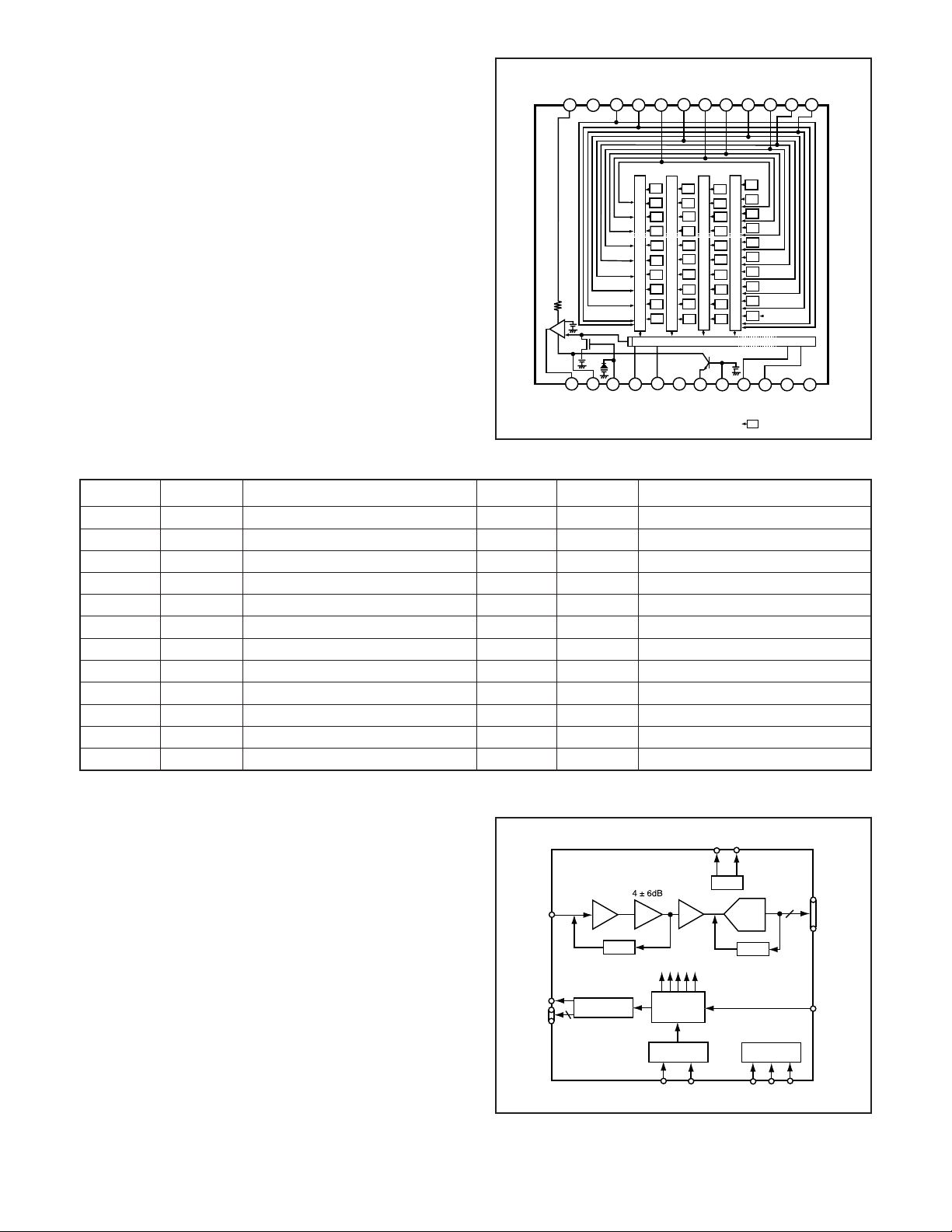
2. IC901 (CCD imager)
[Structure]
Interline type CCD image sensor
Image size Diagonal 6.67 mm (1/2.7 type)
Pixels in total 2396 (H) x 1766 (V)
Recording pixels 2288 (H) x 1712 (V)
Pin No.
1
2
3
4
5
6
7
8
9
10
11
12
Symbol
6
Vø
Vø5B
Vø5A
Vø4
Vø3B
Vø3A
Vø2
Vø1
VøST
VøHLD
GND
GND
Vertical register transfer clock
Vertical register transfer clock
Vertical register transfer clock
Vertical register transfer clock
Vertical register transfer clock
Vertical register transfer clock
Vertical register transfer clock
Vertical register transfer clock
Horizontal addition control clock
Horizontal addition control clock
GND
GND
Pin Description
Pin No.
13
14
15
16
17
18
19
20
21
22
23
24
Gb
B
Gb
Gr
R
B
Gb
Gr
R
B
Gb
Gr
R
B
Gb
Gr
R
B
Gb
Gr
R
Horizontal register
18
19
20
SUB
SUB
GND
C
Ø
(Note) : Photo sensor
OUT
V
R
Gb
R
Gb
R
Gb
Vertical register
R
Gb
R
RG
Ø
17
1615
Ø2B
Ø1B
H
H
1413
DD
V
Fig. 1-1. CCD Block Diagram
Symbol
V
OUT
VDD
øRG
1B
Hø
Hø2B
GND
øSUB
C
SUB
1A
Hø
Hø2A
GND
V
L
Signal output
Circuit power
Reset gate clock
Horizontal register transfer clock
Horizontal register transfer clock
GND
Substrate clock
Substrate bias
Horizontal register transfer clock
Horizontal register transfer clock
GND
Protection transistor bias
Pin Description
B
Gr
B
Gr
B
Gr
B
Gr
B
Gr
(Note)
21
23
24
22
Ø1A
H
L
V
Ø2A
GND
H
Table 1-1. CCD Pin Description
3. IC902, IC903 (V Driver) and IC905 (H driver)
An H driver and V driver are necessary in order to generate
the clocks (vertical transfer clock, horizontal transfer clock
and electronic shutter clock) which driver the CCD.
IC902 and IC903 are V driver. In addition the XV1-XV6 signals which are output from IC101 are the vertical transfer
clocks, and the XSG signal is superimposed at IC902 and
IC903 in order to generate a ternary pulse. In addition, the
XSUB signal which is output from IC101 is used as the sweep
pulse for the electronic shutter. A H driver is inside IC905,
and H1, H2 and RG clock are generated at IC905.
4. IC905 (CDS, AGC Circuit and A/D Converter)
The video signal which is output from the CCD is input to Pin
(27) of IC905. There are inside the sampling hold block, AGC
block and A/D converter block.
The setting of sampling phase and AGC amplifier is carried
out by serial data at Pin (32). The video signal is carried out
A/D converter, and is output by 12-bit.
– 2 –
CCDIN
RG
H1-H4
VRB
VRT
VREF
2~36 dB
VGA
PxGA
CDS
HORIZONTAL
4
DRIVERS
CLAMP
INTERNAL
CLOCKS
PRECISION
TIMING
CORE
SYNC
GENERATOR
VD
HD
Fig. 1-2. IC905 Block Diagram
ADC
CLAMP
INTERNAL
REGISTERS
SL
SCK
10
SDATA
DOUT
CLI
Page 2

1-2. CP1 CIRCUIT DESCRIPTION
1. Circuit Description
1-1. Digital clamp
The optical black section of the CCD extracts averaged values from the subsequent data to make the black level of the
CCD output data uniform for each line. The optical black section of the CCD averaged value for each line is taken as the
sum of the value for the previous line multiplied by the coefficient k and the value for the current line multiplied by the
coefficient 1-k.
1-2. Signal processor
1. γ correction circuit
This circuit performs (gamma) correction in order to maintain
a linear relationship between the light input to the camera
and the light output from the picture screen.
2. Color generation circuit
This circuit converts the CCD data into RGB signals.
3. Matrix circuit
This circuit generates the Y signals, R-Y signals and B-Y signals from the RGB signals.
4. Horizontal and vertical aperture circuit
This circuit is used gemerate the aperture signal.
1-3. AE/AWB and AF computing circuit
The AE/AWB carries out computation based on a 64-segment
screen, and the AF carries out computations based on a 6segment screen.
1-4. SDRAM controller
This circuit outputs address, RAS, CAS and AS data for controlling the SDRAM. It also refreshes the SDRAM.
1-5. Communication control
1. SIO
This is the interface for the 8-bit microprocessor.
2. PIO/PWM/SIO for LCD
8-bit parallel input and output makes it possible to switch between individual input/output and PWM input/output.
1-6. TG/SG
Timing generated for 4 million pixel horizontal addtion CCD
control.
1-7. Digital encorder
It generates chroma signal from color difference signal.
2. Outline of Operation
When the shutter opens, the reset signals (ASIC and CPU)
and the serial signals (“take a picture” commands) from the
8-bit microprocessor are input and operation starts.
When the TG/SG drives the CCD, picture data passes through
the A/D and CDS, and is then input to the ASIC as 12-bit
data. The AF, AE, AWB, shutter, and AGC value are computed from this data, and three exposures are made to obtain
the optimum picture. The data which has already been stored
in the SDRAM is read by the CPU and color generation is
carried out. Each pixel is interpolated from the surrounding
data as being either Ye, Cy, Mg or B primary color data to
produce R, G and B data. At this time, correction of the lens
distortion which is a characteristic of wide-angle lenses is
carried out. After AWB and γ processing are carried out, a
matrix is generated and aperture correction is carried out for
the Y signal, and the data is then compressed by JPEG and
is then written to card memory (SD card).
When the data is to be output to an external device, it is taken
data from the memory and output via the USB I/F. When played
back on the LCD and monitor, data is transferred from memery
to the SDRAM, and the image is then elongated so that it is
displayed over the SDRAM display area.
3. LCD Block
LCD block is in the CP1 board, and it is constructed by VCOM
gerenated circuit etc. The video signal from the ASIC are input to LCD panel directly by 6-bit digital signal, and are converted into RGB signals by driver circuit in the LCD panel.
Because the LCD closes more as the difference in potential
between the VCOM (common polar voltage: AC) and the R,
G and B signals becomes greater, the display becomes darker;
if the difference inpotential is smaller, the element opens and
the LCD becomes brighter. And also timing pulse except video
signal are input at LCD panel directly from ASIC.
4. Lens drive block
4-1. Iris drive
When the drive signals (AMIN_A and AMIN_-A) which are output from the ASIC (IC101), it is driven by the driver (IC951),
and are then used to drive the iris steps.
4-2. Focus drive
When the drive signals (FIN_A, FIN_-A, FIN_B and FIN_-B)
which are output from the ASIC expansion I/O port (IC106),
the focus stepping motor is driven by the driver (IC951). Detection of the standard focusing positions is carried out by
means of the photointerruptor (FOCUS PI) inside the lens block.
4-3. Zoom drive
When the drive signals (ZIN_A, ZIN_-A, ZIN_B and ZIN_-B)
which are output from the ASIC (IC101), the zoom stepping
motor is driven by the driver (IC951). Detection of the standard
zoom positions is carried out by means of photointerruptor
(ZOOM PI) inside the lens block.
4-4. Shutter drive
When the drive signals (SMIN_A and SMIN_-A) which are output from the ASIC (IC101), it is driven regular current by the
driver (IC951).
– 3 –
Page 3

1-3. ST1 POWER CIRCUIT DESCRIPTION
1. Outline
This is the main power circuit, and is comprised of the following blocks.
Switching power controller (IC501)
Analog system power output (Q5001, T5001)
Digital 1.8 V power output (L5006)
Digital 3.3 V power output (L5005)
LCD 15 V power output (Q5015, L5007)
LED backlight power output (Q5003, L5009)
5 V system power output (L5004)
4.7 V lens system power output (IC955, Q9552, L9551)
2. Switching Controller
This is the basic circuit which is necessary for controlling the
power supply for a PWM-type switching regulator, and is provided with five built-in channels, only CH1 (analog system
power output), CH2 (LCD 15 V power output), CH_M (digital
3.3 V system power output), CH_SD (digital 1.8 V system
power output), CH3 (LED back light power output) and CH_SU
(5 V system power output) are used. Feedback from 15.0 V
(A) (CH1), 15 V (L) (CH2), 3.3 V (D) (CH_M), 1.8 V (D)
(CH_SD), LED backlight output (CH3) and 5 V (CH_SU) power
supply outputs are received, and the PWM duty is varied so
that each one is maintained at the correct voltage setting level.
2-1. Short-circuit Protection
If output is short-circuited for the length of time setting inside
IC501, all output is turned off. The control signal (P ON) are
recontrolled to restore output.
3. Analog System Power Output
15.0 V (A), -7.6 V (A) and 3.45 V (A) are output. Feedback for
the 15.0 V (A) is provided to the switching controller (Pin (3)
of IC501) so that PWM control can be carried out.
4. Digital 1.8 V Power Output
1.8 V (D) is output. Feedback for the 1.8 V (D) is provided to
the switching controller (Pins (9) of IC501) so that PWM control can be carried out.
5. Digital 3.3 V Power Output
3.3 V (D) is output. Feedback for the 3.3 V (D) is provided to
the swiching controller (Pin (13) of IC501) so that PWM control can be carried out.
6. LCD 15 V Power Output
LCD 15 V (L) is output. Feedback for the 15 V (L) is provided
to the swiching controller (Pin (31) of IC501) so that PWM
control can be carried out.
7. LED Backlight Power Output
A constant current flows to LCD 8.5 V (L) power and the backlight LEDs. Feedback for the voltage of R5047 and R5048
are provided to the power controller (Pin (39) of IC501) so
that PWM control can be carried out.
8. 5 V System Power Output
5 V is output. Feedback for the 5 V is provided to the swiching
controller (Pin (17) of IC501) so that PWM control can be
carried out.
9. 4.7 V Lens System Power Output
Lens power (4.7 V) is output. Feedback for the BOOST 4.7 V
is provided to the swiching controller (Pin (1) of IC955) so
that PWM control can be carried out.
– 4 –
Page 4

1-4. ST1 STROBE CIRCUIT DESCRIPTION
1. Charging Circuit
When UNREG power is supplied to the charge circuit and the
CHG signal from microprocessor becomes High (3.3 V), the
charging circuit starts operating and the main electorolytic
capacitor is charged with high-voltage direct current.
However, when the CHG signal is Low (0 V), the charging
circuit does not operate.
1-1. Charge switch
When the CHG signal switches to Hi, IC541 starts charging
operation.
1-2. Power supply filter
C5401 constitutes the power supply filter. They smooth out
ripples in the current which accompany the switching of the
oscillation transformer.
1-3. Oscillation circuit
This circuit generates an AC voltage (pulse) in order to increase the UNREG power supply voltage when drops in current occur. This circuit generates a drive pulse with a frequency
of approximately 150-250 kHz. Because self-excited light omission is used, the oscillation frequency changes according to
the drive conditions.
2. Light Emission Circuit
When FLCLT signal is input from the ASIC expansion port,
the stroboscope emits light.
2-1. Emission control circuit
When the FLCLT signal is input to the emission control circuit, Q5409 switches on and preparation is made to the light
emitting. Moreover, when a FLCLT signal becomes Lo, the
stroboscope stops emitting light.
2-2. Trigger circuit
The Q5409 is turned ON by the FLCLT signal and light emission preparation is preformed. Simultaneously, high voltage
pulses of several kV are emitted from the trigger coil and applied to the light emitter.
2-3. Light emitting element
When the high-voltage pulse form the trigger circuit is applied to the light emitting part, currnet flows to the light emitting element and light is emitted.
Beware of electric shocks.
1-4. Oscillation transformer
The low-voltage alternating current which is generated by the
oscillation control circuit is converted to a high-voltage alternating current by the oscillation transformer.
1-5. Rectifier circuit
The high-voltage alternating current which is generated at
the secondary side of T5401 is rectified to produce a highvoltage direct current and is accumulated at electrolytic capacitor C5412.
1-6. Voltage monitoring circuit
The functions programmed in the IC541 monitor oscillations
and estimate the charging voltage. If the voltage exceeds the
rated value, charging automatically stops. Then, the CHGDONE signal is changed to Lo output and a "charging stopped"
signal is sent to the microcomputer.
– 5 –
Page 5

1-5. SYA CIRCUIT DESCRIPTION
1. Configuration and Functions
For the overall configuration of the SYA block, refer to the block diagram. The SYA block centers around a 8-bit microprocessor
(IC301), and controls camera system condition (mode).
The 8-bit microprocessor handles the following functions.
1. Operation key input, 2. Clock control and backup, 3. Power ON/OFF, 4. Storobe charge control, 5. Signal input and output for
zoom and lens control.
Pin
1
2
3
4
5
6
7
8
9
10
11
12
13
14
15
16
17
18
19
20
21 LCD ON2
22 LCD ON
23 BLON
24
25 PRG SO
26
27
28
29
30
31
32
33
34
35
36
37
38
39
40
41
42~44
Signal
AVREF
AVSS
IC
VDD
REGC
VSS
XIN
XOUT
RESET
XCIN
XCOUT
CLKSEL0
BAT_OFF
NC
USB_DET
BR_OPEN
SREQ
BACKUP_CTL
LCD ON3
FLMD1
NC
PRG SI
PRG SCK
MAIN RESET
NC
VF. LED (R)
VF. LED (G)
VSS
VDD
P ON
PA O N
SCK
SI
SO
CHG ON
FLMD0
NC
SCAN OUT 2~0
I/O
O
O
O
O
O
O
O
O
O
O
O
O
O
O
O
O
O
O
O
O
O
O
O
Outline
I
-
-
-
-
-
I
-
I
I
-
I
I
I
I
I
-
-
I
Analog standard voltage input terminal
GND
Power for program writing
VDD
Regulator output stability capacity connection
GND
Main clock oscillation terminal (4MHz)
Main clock oscillation terminal
Reset input
Clock oscillation terminal (32.768 kHz)
Clock oscillation terminal
ARM system clock ON/OFF
Battery off detection signal input
(Output mode “0” fixing)
USB power detection terminal ( ↓ detection)
Manual barrrier detection ( ↓ detection)
Communication transmission clock (SY-ASIC)
Backup battery charge control (L= charge)
D/D converter (LCD system) ON/OFF signal 3
Flash writing control 1
D/D converter (LCD system) ON/OFF signal 2
D/D converter (LCD system) ON/OFF signal 1
LCD backlight ON signal (H= lighting)
(Output mode “0” fixing)
Serial data output for flash
Serial data input for flash
Serial clock output for flash
System reset (MRST)
(Output mode “0” fixing)
VF LED (red) (L= lighting)
VF LED (green) (L= lighting)
GND
VDD
D/D converter (digital system) ON/OFF signal
D/D converter (analog system) ON/OFF signal
Serial clock output
Serial data input
Serial data output
Strobe charge control
Flash writing contol 0
(Output mode “0” fixing)
Key matrix output
See next page
– 6 –
Page 6

45
46
47
48
49
50
51~56
57
58
59
60
61
62
63
64
BOOT_COMREQ O
NC O
CARD
AVREF ON
PLLEN
ASIC TEST
SCAN IN5~0
NC
DC_IN
AV_JACK
CHG_DONE I
NC
INT_TEMP
NC
BATTERY
Table 5-1. 8-bit Microprocessor Port Specification
Boot/command request
(Output mode “0” fixing)
I Card detection (L= card)
O
O
O
O
I
I
I
I
I
I
I
AD VREF ON/OFF signal (L= ON)
ASIC PLL oscillation ON/OFF
ASIC control signal (ZTEST)
Key scan input 5~0
DC adaptor connection detecion (L= DC adaptor)
AV JACK connection detection (H= AV JACK detection)
Storobe charge detection (input port) (L= ON)
Internal temperature detection (analog)
Battery voltage detection (analog)
2. Internal Communication Bus
The SYA block carries out overall control of camera operation by detecting the input from the keyboard and the condition of the
camera circuits. The 8-bit microprocessor reads the signals from each sensor element as input data and outputs this data to the
camera circuits (ASIC) or to the LCD display device as operation mode setting data. Fig. 5-1 shows the internal communication
between the 8-bit microprocessor, ASIC and SPARC lite circuits.
ZTEST
ASIC RESET
S. REQ
8-bit
Microprocessor
Fig. 5-1 Internal Bus Communication System
ASIC SO
ASIC SI
ASIC SCK
PLLEN
CLKSEL0
3. Key Operaiton
For details of the key operation, refer to the instruction manual.
SCAN
OUT
SCAN
IN
0
1
2
0
← LEFT
MODE
REC (MOV)
1
↑ UP
MENU
REC (CAM)
2
↓ DOWN
TELE
PLAY
3
→ RIGHT
WIDE
4
SET
1st SHUTTER
ASIC
5
TEST
2nd SHUTTER
Table 5-2. Key Operation
– 7 –
Page 7

4. Power Supply Control
The 8-bit microprocessor controls the power supply for the overall system.
The following is a description of how the power supply is turned on and off. When the battery is attached, a regulated 3.2 V
voltage is normally input to the 8-bit microprocessor (IC301) by IC302, so that clock counting and key scanning is carried out
even when the power switch is turned off, so that the camera can start up again. When the battery is removed, the 8-bit microprocessor operates in sleep mode using the backup lithium secondary battery. At this time, the 8-bit microprocessor only carries
out clock counting, and waits in standby for the battery to be attached again. When a switch is operated, the 8-bit microprocessor
supplies power to the system as required.
The 8-bit microprocessor first sets both the P (A) ON signal at pin (35) and the P ON signal at pin (34) to high, and then turns on
the DC/DC converter. After this, high signals are output from pins (12), (28), (49) and (50) so that the ASIC is set to the active
condition. If the LCD monitor is on, the LCD ON signal at pin (22) and the LCD ON 2 signal at pin (21) set to high, and the DC/DC
converter for the LCD monitor is turned on. Once it is completed, the ASIC returns to the reset condition, all DC/DC converters
are turned off and the power supply to the whole system is halted.
ASIC,
memory
Power voltage
Power OFF
Power switch ON-
Auto power OFF
Shutter switch ON
CAMERA
Monitor OFF
LCD finder
Play back
Table 5-3. Camera Mode (Battery Operation)
Note) 4 MHz = Main clock operation, 32 kHz = Sub clock operation
3.3 V
OFF
OFF
ON
OFF
ON
ON
CCD
5 V (A)
+15 V (A) etc.
OFF
OFF
ON→OFF
OFF
ON
OFF
3.2 V
(ALWAYS)
32KHz OFF
4 MHz OFF
4 MHz OFF
4 MHz OFF
4 MHz ON
4 MHz ON
5. 16-bit A/D circuit (Audio)
This circuit converts the audio signals (analog signals) from the microphone to 16-bit digital signals.
8 bit
CPU
LCD
MONITOR
+15 V (L)
6. 16-bit D/A circuit (Audio)
The audio signals which were converted to digial form by the 16-bit A/D circuit are temporarily to a sound buffer and then
recorded in the SSFDC card. During playback, the 16-bit D/A circuit converts these signals into analog audio signals.
– 8 –
 Loading...