

Page 1
SERVICE MANUAL
FILE NO.
Digital Camera
Contents
1. OUTLINE OF CIRCUIT DESCRIPTION .................... 2
2. DISASSEMBLY .......................................................... 9
3. ELECTRICAL ADJUSTMENT .................................. 12
4. USB STORAGE INFORMATION
REGISTRATION ...................................................... 16
5. TROUBLESHOOTING GUIDE................................. 17
6. PARTS LIST............................................................. 18
CABINET AND CHASSIS PARTS 1 ........................ 18
CABINET AND CHASSIS PARTS 2 ........................ 19
ELECTRICAL PARTS .............................................. 20
ACCESSORIES ....................................................... 25
PACKING MATERIALS............................................ 25
CIRCUIT DIAGRAMS &
PRINTED WIRING BOARDS ...................................... C1
VPC-J1
(Product Code : 126 626 01)
(U.S.A)
(Canada)
VPC-J1EX
(Product Code : 126 626 02)
(Europe)
(PAL General)
PRODUCT SAFETY NOTICE
The components designated by a symbol ( ! ) in this schematic diagram designates components whose value are of
special significance to product safety. Should any component designated by a symbol need to be replaced, use only the part
designated in the Parts List. Do not deviate from the resistance, wattage, and voltage ratings shown.
CAUTION : Danger of explosion if battery is incorrectly replaced.
Replace only with the same or equivalent type recommended by the manufacturer.
Discard used batteries according to the manufacturer’s instructions.
NOTE : 1. Parts order must contain model number, part number, and description.
2. Substitute parts may be supplied as the service parts.
3. N. S. P. : Not available as service parts.
Design and specification are subject to change without notice.
SX711/U, EX
REFERENCE No. SM5310497
Page 2
1. OUTLINE OF CIRCUIT DESCRIPTION
1-1. CA1 and A PART OF CP1 CIRCUIT
DESCRIPTIONS
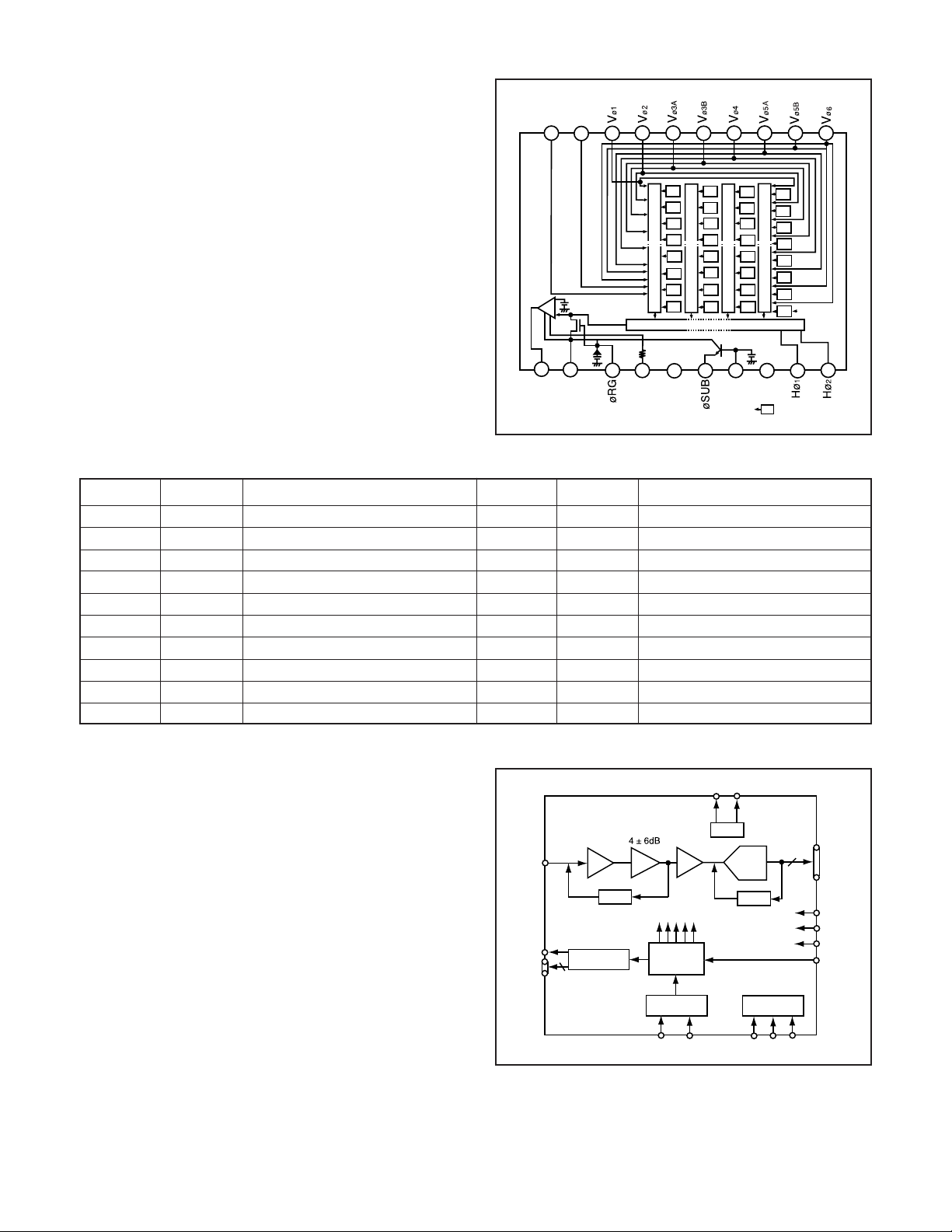
Around CCD block
1. IC Configuration
CA1 board
IC901 (ICX451DQF) CCD imager
CP1 board
IC931 (H driver, CDS, AGC and A/D converter)
2. IC901 (CCD imager)
[Structure]
Interline type CCD image sensor
Image size Diagonal 6.67 mm (1/2.7 type)
Pixels in total 2140 (H) x 1564 (V)
Recording pixels 2048 (H) x 1536 (V)
11
VHLD
10
OUT
V
12
DD
V
VST
9
13
7
8
6
Gb
R
Gb
R
Gb
R
Vertical register
Gb
R
14
15
GND
Horizontal register
Fig. 1-1. CCD Block Diagram
3
4
5
B
Gb
Gr
R
B
Gb
Gr
R
B
Gb
Gr
R
B
Gb
Gr
R
17
16
GND
18
L
V
SUB
C
(Note) : Photo sensor
1
2
B
Gr
B
Gr
B
Gr
B
(Note)
Gr
20
19
Pin No.
1
2
3
4
5
6
7
8
9
10
Symbol
6
Vø
Vø5B
Vø5A
Vø4
Vø3B
Vø3A
Vø2
Vø1
VST
VHLD
Vertical register transfer clock
Vertical register transfer clock
Vertical register transfer clock
Vertical register transfer clock
Vertical register transfer clock
Vertical register transfer clock
Vertical register transfer clock
Vertical register transfer clock
Horizontal addition control clock
Horizontal addition control clock
Pin Description
Table 1-1. CCD Pin Description
3. IC934, IC935 (V Driver) and IC931 (H driver)
An H driver and V driver are necessary in order to generate
the clocks (vertical transfer clock, horizontal transfer clock
and electronic shutter clock) which driver the CCD.
IC934 and IC935 are V driver. In addition the XV1-XV6 signals which are output from IC101 are the vertical transfer
clocks, and the XSG signal is superimposed at IC934 and
IC935 in order to generate a ternary pulse. In addition, the
XSUB signal which is output from IC101 is used as the sweep
pulse for the electronic shutter. A H driver is inside IC931,
and H1, H2 and RG clock are generated at IC931.
Pin No.
11
12
13
14
15
16
17
18
19
20
CCDIN
RG
H1-H4
Symbol
V
OUT
VDD
øRG
GND
GND
øSUB
CSUB
V
Hø1
Hø2
CDS
HORIZONTAL
4
DRIVERS
L
CLAMP
Pin Description
Signal output
Circuit power
Reset gate clock
GND
GND
Substrate clock
Substrate bias
Protection transistor bias
Horizontal register transfer clock
Horizontal register transfer clock
VRB
VRT
VREF
PxGA
2~36 dB
VGA
INTERNAL
CLOCKS
PRECISION
TIMING
CORE
ADC
CLAMP
12
DOUT
CLPOB
CLPDM
PBLK
CLI
4. IC931 (CDS, AGC Circuit and A/D Converter)
The video signal which is output from the CCD is input to Pin
(29) of IC931. There are inside the sampling hold block, AGC
block and A/D converter block.
The setting of sampling phase and AGC amplifier is carried
out by serial data at Pin (37) of IC911. The video signal is
carried out A/D converter, and is output by 10-bit.
– 2 –
SYNC
GENERATOR
VD
HD
INTERNAL
REGISTERS
SL
SCK
Fig. 1-2. IC931 Block Diagram
SDATA
Page 3

1-2. CP1 CIRCUIT DESCRIPTION
1. Circuit Description
1-1. Digital clamp
The optical black section of the CCD extracts averaged values from the subsequent data to make the black level of the
CCD output data uniform for each line. The optical black section of the CCD averaged value for each line is taken as the
sum of the value for the previous line multiplied by the coefficient k and the value for the current line multiplied by the
coefficient 1-k.
1-2. Signal processor
1. γ correction circuit
This circuit performs (gamma) correction in order to maintain
a linear relationship between the light input to the camera
and the light output from the picture screen.
2. Color generation circuit
This circuit converts the CCD data into RGB signals.
3. Matrix circuit
This circuit generates the Y signals, R-Y signals and B-Y signals from the RGB signals.
4. Horizontal and vertical aperture circuit
This circuit is used gemerate the aperture signal.
1-3. AE/AWB and AF computing circuit
The AE/AWB carries out computation based on a 64-segment
screen, and the AF carries out computations based on a 6segment screen.
1-4. SDRAM controller
This circuit outputs address, RAS, CAS and AS data for controlling the SDRAM. It also refreshes the SDRAM.
1-5. Communication control
1. SIO
This is the interface for the 8-bit microprocessor.
2. PIO/PWM/SIO for LCD
8-bit parallel input and output makes it possible to switch between individual input/output and PWM input/output.
1-6. TG/SG
Timing generated for 3 million pixel horizontal addtion CCD
control.
1-7. Digital encorder
It generates chroma signal from color difference signal.
2. Outline of Operation
When the shutter opens, the reset signals (ASIC and CPU)
and the serial signals (“take a picture” commands) from the
8-bit microprocessor are input and operation starts.
When the TG/SG drives the CCD, picture data passes through
the A/D and CDS, and is then input to the ASIC as 10-bit
data. The AF, AE, AWB, shutter, and AGC value are computed from this data, and three exposures are made to obtain
the optimum picture. The data which has already been stored
in the SDRAM is read by the CPU and color generation is
carried out. Each pixel is interpolated from the surrounding
data as being either Ye, Cy, Mg or B primary color data to
produce R, G and B data. At this time, correction of the lens
distortion which is a characteristic of wide-angle lenses is
carried out. After AWB and γ processing are carried out, a
matrix is generated and aperture correction is carried out for
the Y signal, and the data is then compressed by JPEG and
is then written to card memory (SD card).
When the data is to be output to an external device, it is taken
data from the memory and output via the USB I/F. When played
back on the LCD and monitor, data is transferred from memery
to the SDRAM, and the image is then elongated so that it is
displayed over the SDRAM display area.
3. LCD Block
LCD block is in the CP1 board, and it is constructed by VCOM
gerenated circuit etc. The video signal from the ASIC are input to LCD panel directly by 6-bit digital signal, and are converted into RGB signals by driver circuit in the LCD panel.
Because the LCD closes more as the difference in potential
between the VCOM (common polar voltage: AC) and the R,
G and B signals becomes greater, the display becomes darker;
if the difference inpotential is smaller, the element opens and
the LCD becomes brighter. And also timing pulse except video
signal are input at LCD panel directly from ASIC.
4. Lens drive block
4-1. Iris drive
When the drive signals (AMIN_A and AMIN_-A) which are output from the ASIC (IC101), it is driven by the driver (IC951),
and are then used to drive the iris steps.
4-2. Focus drive
When the drive signals (FIN_A, FIN_-A, FIN_B and FIN_-B)
which are output from the ASIC expansion I/O port (IC105),
the focus stepping motor is driven by the driver (IC951). Detection of the standard focusing positions is carried out by
means of the photointerruptor (FOCUS PI) inside the lens block.
4-3. Zoom drive
When the drive signals (ZIN_A, ZIN_-A, ZIN_B and ZIN_-B)
which are output from the ASIC (IC101), the zoom stepping
motor is driven by the driver (IC951). Detection of the standard
zoom positions is carried out by means of photointerruptor
(ZOOM PI) inside the lens block.
4-4. Shutter drive
When the drive signals (SMIN_A and SMIN_-A) which are output from the ASIC (IC101), it is driven regular current by the
driver (IC951).
– 3 –
Page 4

1-3. PW1 POWER CIRCUIT DESCRIPTION
1. Outline
This is the main power circuit, and is comprised of the following blocks.
Switching power controller (IC501)
Analog system power output (Q5001, T5001)
Digital 1.8 V power output (Q5011, L5007)
Digital 3.3 V power output (Q5010, L5005)
LED backlight power output (Q5015, L5010)
5 V system power output (Q5018, L5017)
2. Switching Controller
This is the basic circuit which is necessary for controlling the
power supply for a PWM-type switching regulator, and is provided with five built-in channels, only CH1 (analog system
power output), CH2 (digital 3.3 V system power output), CH3
(digital 1.8 V system power output), CH4 (LED back light power
output) and CH5 (5 V system power output) are used. Feedback from 15.0 V (A) (CH1), 3.3 V (D) (CH2), 1.8 V (D) (CH3),
LED backlight output (CH4) and 5 V (CH5) power supply outputs are received, and the PWM duty is varied so that each
one is maintained at the correct voltage setting level.
2-1. Short-circuit Protection
If output is short-circuited for the length of time determined
by the condenser which is connected to Pin (27) of IC501, all
output is turned off. The control signal (P ON) are recontrolled
to restore output.
3. Analog System Power Output
15.0 V (A) and -7.6 V (A) are output. Feedback for the 15.0 V
(A) is provided to the switching controller (Pin (23) of IC501)
so that PWM control can be carried out.
4. Digital 1.8 V Power Output
1.8 V (D) is output. Feedback for the 1.8 V (D) is provided to
the switching controller (Pins (15) of IC501) so that PWM control can be carried out.
5. Digital 3.3 V Power Output
3.3 V (D) is output. Feedback for the 3.3 V (D) is provided to
the swiching controller (Pin (42) of IC501) so that PWM control can be carried out.
6. LED Backlight Power Output
A constant current flows to the backlight LEDs. Feedback for
the voltage of R5057 is provided to the power controller (Pin
(18) of IC501) so that PWM control can be carried out.
7. 5 V System Power Output
5 V is output. Feedback for the 5 V is provided to the swiching
controller (Pin (39) of IC501) so that PWM control can be
carried out.
– 4 –
Page 5

1-4. ST1 STROBE CIRCUIT DESCRIPTION
1. Charging Circuit
When UNREG power is supplied to the charge circuit and the
CHG signal from microprocessor becomes High (3.3 V), the
charging circuit starts operating and the main electorolytic
capacitor is charged with high-voltage direct current.
However, when the CHG signal is Low (0 V), the charging
circuit does not operate.
1-1. Power switch
When the CHG signal switches to Hi, Q5407 turns ON and
the charging circuit starts operating.
1-2. Power supply filter
C5401 constitutes the power supply filter. They smooth out
ripples in the current which accompany the switching of the
oscillation transformer.
1-3. Oscillation circuit
This circuit generates an AC voltage (pulse) in order to increase the UNREG power supply voltage when drops in current occur. This circuit generates a drive pulse with a frequency
of approximately 50-100 kHz. Because self-excited light omission is used, the oscillation frequency changes according to
the drive conditions.
2. Light Emission Circuit
When RDY and TRIG signals are input from the ASIC expansion port, the stroboscope emits light.
2-1. Emission control circuit
When the RDY signal is input to the emission control circuit,
Q5409 switches on and preparation is made to let current
flow to the light emitting element. Moreover, when a STOP
signal is input, the stroboscope stops emitting light.
2-2. Trigger circuit
When a TRIG signal is input to the trigger circuit, D5405
switches on, a high-voltage pulse of several kilovolts is generated inside the trigger circuit, and this pulse is then applied
to the light emitting part.
2-3. Light emitting element
When the high-voltage pulse form the trigger circuit is applied to the light emitting part, currnet flows to the light emitting element and light is emitted.
Beware of electric shocks.
1-4. Oscillation transformer
The low-voltage alternating current which is generated by the
oscillation control circuit is converted to a high-voltage alternating current by the oscillation transformer.
1-5. Rectifier circuit
The high-voltage alternating current which is generated at
the secondary side of T5401 is rectified to produce a highvoltage direct current and is accumulated at electrolytic capacitor C5512.
1-6. Voltage monitoring circuit
This circuit is used to maintain the voltage accumulated at
C5512 at a constance level.
After the charging voltage is divided and converted to a lower
voltage by R5417, R5419 and R5420, it is output to the microprocessor as the monitoring voltage VMONIT. When this
VMONIT voltage reaches a specified level at the microprocessor, the CHG signal is switched to Low and charging is
interrupted.
– 5 –
Page 6

1-5. SYA CIRCUIT DESCRIPTION
1. Configuration and Functions
For the overall configuration of the SYA block, refer to the block diagram. The SYA block centers around a 8-bit microprocessor
(IC301), and controls camera system condition (mode).
The 8-bit microprocessor handles the following functions.
1. Operation key input, 2. Clock control and backup, 3. Power ON/OFF, 4. Storobe charge control, 5. Signal input and output for
zoom and lens control.
Pin
1~3
4
5
6
7
8
9
10
11
12
13
14
15
16
17
18
19
20
21
22
23
24 VDD
25 AVSS
26~29 SCAN IN 0~3
30
31
32
33
34
35
36
37
38
39
40
41
42
43
44
45
46
47
/STBY_LED (GREEN)
Signal
/SCAN OUT 0~2
/SCAN OUT 3
P ON
PA O N
/STILL_LED
/CSTILL_LED
VSS
VDD
/MOVIE_LED
/STBY_LED (RED)
/AVREF_ON
SI
SO
SCK
PRG SI
PRG SO
PRG SCK
LCD_ON
BLON
CHG ON
INT_TEMP
NOT USED
CHG VOL
BATTERY
AVREF
AVDD
/RESET
XCOUT
XCIN
IC
XOUT
XIN
VSS
/BAT OFF
/SREQ
/SCAN IN6
CLOSE
/DC_IN
I/O
O
O
O
O
O
O
O
O
O
O
O
I/O
O
I/O
O
O
O
O
O
Outline
Key scan output
Lens barrier open/close detection switch for scan output
Digital power ON/OFF control H : ON
Analog power ON/OFF control H : ON
Still image mode LED (orange) control L : ON
Video clip mode LED (orange) control L : ON
-
-
I
I
-
-
I
I
-
I
I
-
-
I
I
I
I
-
I
I
I
I
I
GND
VDD
Video clip mode LED (orange) control L : ON
Stand-by LED (green) control L : ON
Stand-by LED (red) control L : ON
A/D converter standard voltage control L : ON
Receiving data (from ASIC)
Sending data (to ASIC)
Communication clock (to ASIC)
Flash memory writing receiving data
Flash memory writing sending data
Flash memory writing communication clock
LCD power ON/OFF control 1 H : ON
LCD backlight ON/OFF control H : ON
Flash charge control H : ON
VDD
AVSS
Key scan input
Internal temperature detection input (analog input)
-
Storobe charge voltage detection (analog input)
Battery voltage detection (analog input)
Analog standard voltage input terminal
A/D converter analog power terminal
Reset input
Clock oscillation terminal (37.768 kHz)
Clock oscillation terminal
Flash memory writing voltage
Main clock oscillation terminal (4MHz)
Main clock oscillation terminal
GND
Battery OFF detection
Serial communication requirement (from ASIC)
Key scan input 6
Lens barrier close detection switch input
DC jack/battery detection input
See next page →
– 6 –
Page 7
48
49
50
51
52
53
54
55
56
57
58 BR_OPEN
59
60
61
62
63
64
BOOT
AV JAC K I
OPEN
/CARD
NOT USED
LCD ON2
/SCAN_IN 4
/SCAN_IN 5
/BACKUP_CNT
/USB
BR CLOSE O Lens barrier close control H : Close
CLKSEL 0
CLKSEL 1
PLLEN
ZTEST
/ASIC RESET
I/O
I Lens barrier open detection switch input
I
-
O
I
I
O
I
O
O
O CPU clock swtich control
O PLL reset signal L : RESET
O
O
Table 5-1. 8-bit Microprocessor Port Specification
Compulsion boot control L : DC JACK detection
AV jack connection detection H : AV jack detection
SD card insertion detection L : Insertion
-
LCD power ON/OFF control 2
Key scan input 4
Key scan input 5
Backup battery charge control L : Charge ON
USB connector detection L : USB detecion
Lens barrier open control H : Open
CPU clock ON/OFF control H : ON
ASIC reset signal L : RESET
CPU reset singal L : RESET
2. Internal Communication Bus
The SYA block carries out overall control of camera operation by detecting the input from the keyboard and the condition of the
camera circuits. The 8-bit microprocessor reads the signals from each sensor element as input data and outputs this data to the
camera circuits (ASIC) or to the LCD display device as operation mode setting data. Fig. 5-1 shows the internal communication
between the 8-bit microprocessor, ASIC and SPARC lite circuits.
ZTEST
ASIC RESET
S. REQ
8-bit
Microprocessor
Fig. 5-1 Internal Bus Communication System
ASIC SO
ASIC SI
ASIC SCK
PLLEN
CLKSEL0
CLKSEL1
3. Key Operaiton
For details of the key operation, refer to the instruction manual.
SCAN
OUT
SCAN
IN
0
1
2
0
← LEFT
MODE
REC
1
↑ UP
MENU
REC (VF)
2
↓ DOWN
FLASH
PC CAM
3
→ RIGHT
SET
PLAY
4
WIDE
1st SHUTTER
OPTION
ASIC
5
TELE
2nd SHUTTER
COM
6
TEST
POWER OFF
Table 5-2. Key Operation
– 7 –
Page 8
4. Power Supply Control
The 8-bit microprocessor controls the power supply for the overall system.
The following is a description of how the power supply is turned on and off. When the battery is attached, a regulated 3.2 V
voltage is normally input to the 8-bit microprocessor (IC301) by IC302, so that clock counting and key scanning is carried out
even when the power switch is turned off, so that the camera can start up again. When the battery is removed, the 8-bit microprocessor operates in sleep mode using the backup lithium secondary battery. At this time, the 8-bit microprocessor only carries
out clock counting, and waits in standby for the battery to be attached again. When a switch is operated, the 8-bit microprocessor
supplies power to the system as required.
The 8-bit microprocessor first sets both the P (A) ON signal at pin (6) and the P ON signal at pin (5) to high, and then turns on the
DC/DC converter. After this, high signals are output from pins (60), (61), (62), (63) and (64) so that the ASIC is set to the active
condition. If the LCD monitor is on, the LCD ON signal at pin (21) and the LCD ON 2 signal at pin (53) set to high, and the DC/DC
converter for the LCD monitor is turned on. Once it is completed, the ASIC returns to the reset condition, all DC/DC converters
are turned off and the power supply to the whole system is halted.
ASIC,
memory
Power voltage
Power OFF
Power switch ON-
Auto power OFF
Shutter switch ON
CAMERA
Monitor OFF
LCD finder
Play back
Table 4-3. Camera Mode (Battery Operation)
Note) 4 MHz = Main clock operation, 32 kHz = Sub clock operation
3.3 V
OFF
OFF
ON
OFF
ON
ON
CCD
5 V (A)
+15 V (A) etc.
OFF
OFF
ON→OFF
OFF
ON
OFF
3.2 V
(ALWAYS)
32KHz OFF
4 MHz OFF
4 MHz OFF
4 MHz OFF
4 MHz ON
4 MHz ON
5. 16-bit D/A circuit (Audio)
This circuit converts the audio signals (analog signals) from the microphone to 16-bit digital signals.
8 bit
CPU
LCD
MONITOR
+15 V (L)
6. 16-bit A/D circuit (Audio)
The audio signals which were converted to digial form by the 16-bit A/D circuit are temporarily to a sound buffer and then
recorded in the SSFDC card. During playback, the 16-bit D/A circuit converts these signals into analog audio signals.
– 8 –
Page 9
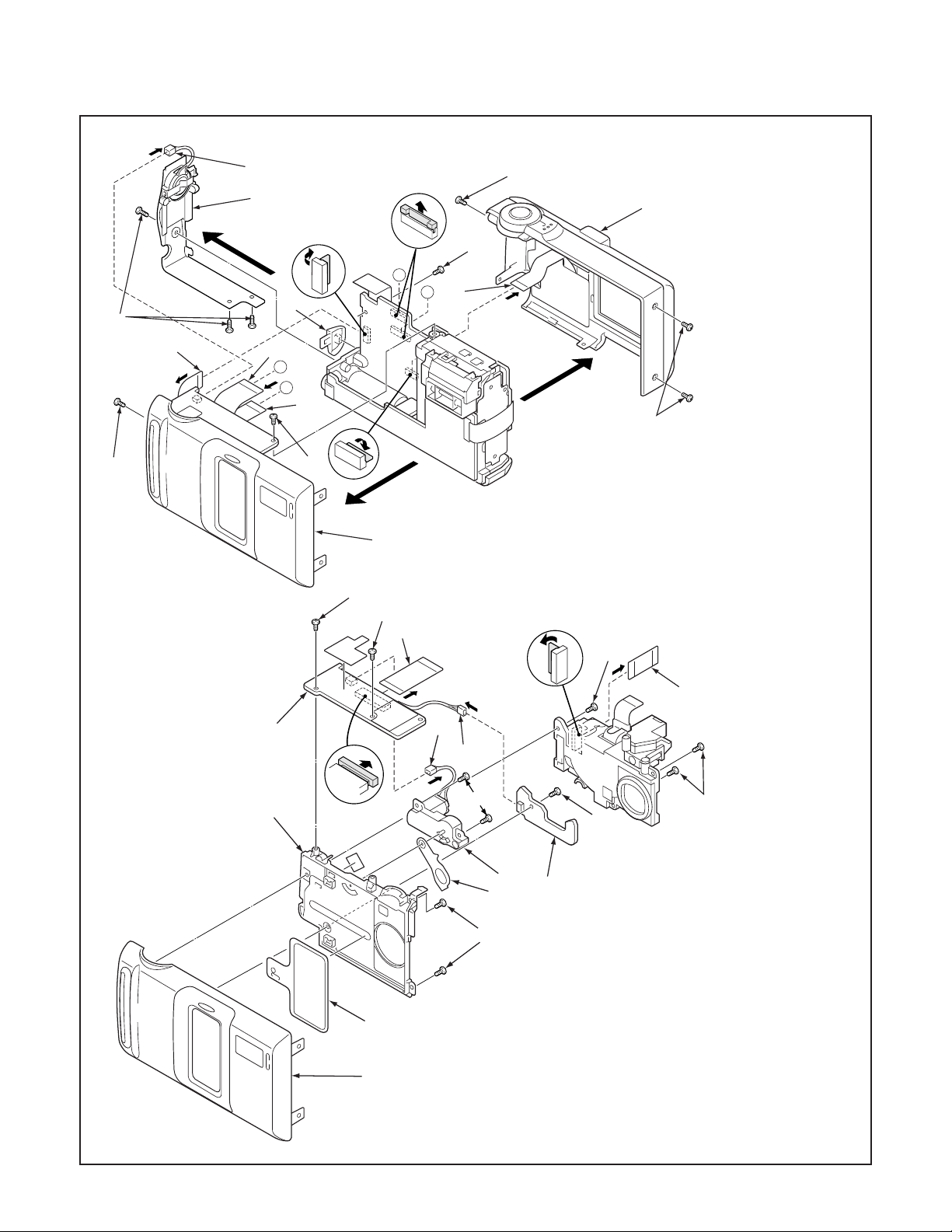
2. DISASSEMBLY
2-1. REMOVAL OF CABINET BACK, CABINET FRONT, CA1 BOARD, TB2 BOARD AND TB1 BOARD
9
10
B
A
3
7
11
7
A
B
7
4
2
5
8
1
1. Two screws 1.7 x 4
2. Two screws 1.7 x 3.5
2
6
3. Three screws 1.7 x 5
4. FPC
5. Cabinet back
6. Screw 1.7 x 3.5
12
7. Three FPCs
8. Screw 1.7 x 3.5
28
28
27
14
9. Connector
10. Cabinet left
11. Cover jack
12. Cabinet front
24
29
26
25
20
18
19
21
22
23
13. Two screws 1.7 x 4
14. Screw 1.7 x 4.5
15. FPC
16. Screw 1.7 x 4.5
17. TB2 board
18. Connector
19. Two screws 1.7 x 4
20. Connector
15
13
16
17
21. Assy motor
22. Lever cover lens
23. Two screws 1.7 x 3.5
24. Cabi front inner
25. Cover lens
26. Cabinet front
27. FFC
28. Two screws 1.7 x 4
29. TB1 board
– 9 –
Page 10
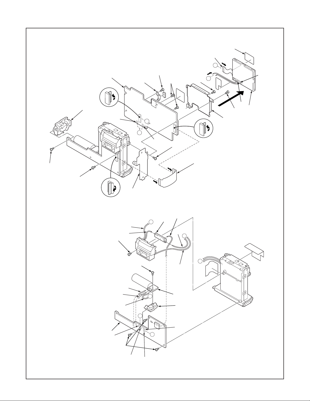
2-2. REMOVAL OF LCD, CP1 BOARD, ST1 BOARD AND ST2 BOARD
11
10
9
8
7
1
2
C
D
5
white
4
red
3
8
14
1. Spacer FPC
2. FPC
3. LCD
4. Screw 1.7 x 3
5. Screw 1.7 x 3.5
6. Holder monitor
7. Two screws 1.7 x 3.5
8. Two screws 1.7 x 3.5
9. Holder terminal
10. Holder USB
11. CP1 board
12. FPC
13. Screw 1.7 x 3.5
14. Screw 1.7 x 3
15. Holder PWB
red
pink (light)
gray (light)
21
gray (deep)
pink (deep)
15
18
C
D
6
white
13
12
gray (deep)
22
G
white
F
E
black
G
19
16. Three screws 1.7 x 3.5
17. ST1 board
18. Screw 1.7 x 3.5
19. ST3 board
20. Stand
21. Screw 1.7 x 3.5
22. ST2 board
pink (light)
17
white
16
black
20
F
blue
E
red
– 10 –
Page 11
2-3. BOARD LOCATION
CA1 board
TB1 board
CP1 board
TB2 board
ST2 board
ST3 board
ST1 board
– 11 –
Page 12
3. ELECTRICAL ADJUSTMENT
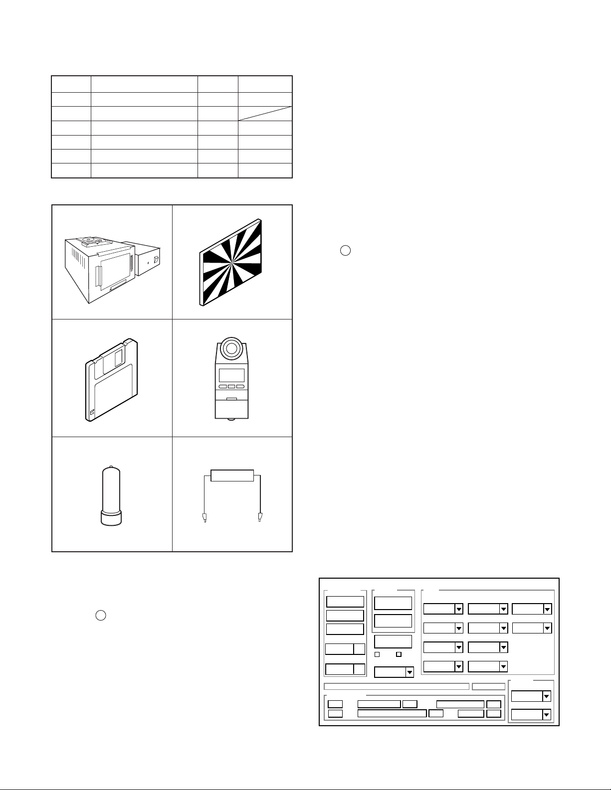
3-1. Table for Servicing Tools
1
1
1
1Chroma meter
1
1
Part code
VJ8-0190
VJ8-0202
VJ8-0192
VJ8-0191
VJ8-0188
Ref. No.
J-1
J-2
J-3
Name
Pattern box (color viewer)
Siemens star chart
Calibration software
Number
J-4
J-5
Spare lump
J-6
Discharge jig
Note: J-1 Pattern box (color viewer) is 100 - 110 VAC only.
3-3. Adjustment Items and Order
1. IC501 Oscillation Frequency Adjustment
2. Lens Adjustment
3. AWB Adjustment
4. CCD White Point Defect Detect Adjustment
5. CCD Black Point And White Point Defect Detect Adjustment In Lighted
6. LCD Panel Adjustment
6-1. LCD VcomPP Adjustment
6-2. LCD VcomDC Adjustment
Note: If the lens, CCD and board in item 2-5, it is necessary
to adjust again.
J-1 J-2
J-3
J-5
J-4
J-6
3-4. Setup
1. System requirements
Windows 98 or Me or 2000 or XP
IBM R -compatible PC with pentium processor
CD-ROM drive
3.5-inch high-density diskette drive
USB port
40 MB RAM
Hard disk drive with at least 15 MB available
VGA or SVGA monitor with at least 256-color display
2. Installing calibration software
1. Insert the calibration software installation diskette into your
diskette drive.
2. Open the explorer.
3. Copy the DscCalDI_130a folder on the floppy disk in the
FD drive to a folder on the hard disk.
3. Installing USB driver
Install the USB driver with camera or connection kit for PC.
4. Pattern box (color viewer)
Turn on the switch and wait for 30 minutes for aging to take
place before using Color Pure. It is used after adjusting the
chroma meter (VJ8-0192) adjust color temperature to 3100 ±
20 K and luminosity to 900 ± 20 cd/m
the lump and its circumference are high temperature during
use and after power off for a while.
2
. Be careful of handling
3-2. Equipment
1. Oscilloscope
2. Digital voltmeter
3. AC adaptor
4. PC (IBM R -compatible PC, Pentium processor, Window
98 or Me or 2000 or XP)
5. Computer screen during adjustment
Calibration
AWB
Focus
UV Matrix
Cal Mode
Cal Data
USB storage
VID
Get
PID
Set
OK
OK
Upload
Firmware
Image
Initialize
EVF
LCD Type
LCD
R Bright
RGB Offset
Tint
VCO
H AFC Test
Serial
Set
– 12 –
Set
Rev.
B Bright
Gain
Phase
Set
Set
VCOMDC
VCOMPP
Setting
Language
Video Mode
Page 13
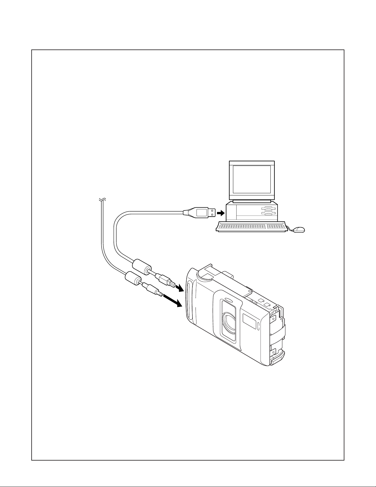
3-5. Connecting the camera to the computer
1. Line up the arrow on the cable connector with the notch on the camera's USB port. Insert the connector.
2. Locate a USB port on your computer.
To USB port
AC adaptor
USB cable
– 13 –
Page 14
3-6. Adjust Specifications
[ST1 board (Side B)]
CL531
VR501
Preparation:
POWER switch: ON
Adjustment condition:
More than A3 size siemens star chart
Fluorescent light illumination with no flicker
Illumination above the subject should be 400 lux ± 10 %.
Adjustment method:
1. Set the siemens star chart 150 cm ± 3 cm so that it becomes center of the screen.
2. Double-click on the DscCalDi.exe.
3. Click the Focus, and click the Yes.
4. Lens adjustment value will appear on the screen.
5. Click the OK.
Note:
1. Frequency adjustment is necessary to repair in the ST1
board and replace the parts. It is carried out with play mode.
Preparation:
1. Remove CN931 in the CP1 board, and lift the cabinet front.
ST1 board can be seen. (Connect all connectors except
CN931.)
2. Insert the SD card.
3. Set the selector dial to playback mode. Comfirm that the
playback image can be seen on the LCD.
1. IC501 Oscillation Frequency Adjustment
Measuring Point
Measuring Equipment
ADJ. Location
ADJ. Value
Adjustment method:
1. Adjust with VR501 to 497.3 ± 1 kHz.
CL531
Frequency counter
VR501
497.3 ± 1 kHz
2. Lens Adjustment
3. AWB Adjustment
Camera
Pattern box
(color viewer)
Preparation:
POWER switch: ON
Adjusting method:
1. When setting the camera in place, set it to an angle so that
nothing appears in any part of the color viewer except the
white section. (Do not enter any light.)
2. Double-click on the DscCalDi.exe.
3. Click the AWB, and click the Yes.
4. AWB adjustment value will appear on the screen.
5. Click the OK.
Camera
Approx.
150 cm 3 cm
Siemens
star chart
4. CCD White Point Defect Detect Adjustment
Preparation:
POWER switch: ON
Adjustment method:
1. Double-click on the DscCalDi.exe.
2. Select “CCD Defect” on the LCD “Test”, and click the “Ye s ”.
3. After the adjustment is completed, OK will display.
4. Click the OK.
– 14 –
Page 15
5. CCD Black Point And White Point Defect Detect
Adjustment In Lighted
Camera
6-1. LCD VcomPP Adjustment
Preparation:
POWER switch: ON
Adjusting method:
1. Double-click on the DscCalDi.exe.
2. Adjust LCD “VCOMPP” so that the amplitude of the CL404
waveform is 5.45 V ± 0.05 Vp-p.
5.45 V
± 0.05 Vp-p
Pattern box
(color viewer)
Preparation:
POWER switch: ON
Setting of pattern box:
Color temperature: 3100 ± 20 (K)
Luminance: 900 ± 20 (cd/m
2
)
Adjusting method:
1. Set the camera 0 cm from the pattern box. (Do not enter
any light.)
2. Double-click on the DscCalDi.exe.
3. Select “CCD Black” on the LCD “Test”, and click the “Ye s ”.
4. After the adjustment is completed, the number of defect
will appear.
6. LCD Panel Adjustment
[CP1 board (Side A)]
CL404 waveform
6-2. LCD VcomDC Adjustment
Adjusting method:
1. Adjust LCD “VCOMDC” so that the amplitude of the CL404
waveform is 4.02 V ± 0.05 Vp-p.
4.02 V
± 0.05 Vp-p
GND
CL404 waveform
CL404
(VCOM)
– 15 –
Page 16

4. USB STORAGE INFORMATION
REGISTRATION
USB storage data is important for when the camera is connected to a computer via a USB connection.
If there are any errors in the USB storage data, or if it has not
been saved, the USB specification conditions will not be satisfied, so always check and save the USB storage data.
Preparation:
POWER switch: ON
Adjustment method:
1. Connect the camera to a computer. (Refer to 3-5. Connecting the camera to the computer on the page 13.)
2. Double-click on the DscCalDi.exe.
3. Click on the Get button in the USB storage window and
check the USB storage data.
VID: SANYO
PID: VPC-J1 or VPC-J1EX
Serial:
Rev. : 1.00
4. Check the “Serial” in the above USB storage data. If the
displayed value is different from the serial number printed
on the base of the camera, enter the number on the base
of the camera. Then click the Set button.
5. Next, check VID, PID and Rev. entries in the USB storage
data. If any of them are different from the values in 3. above,
make the changes and then click the corresponding Set
button.
Calibration
AWB
Focus
UV Matrix
Cal Mode
Cal Data
USB storage
VID
Get
PID
Set
OK
OK
Upload
Firmware
Image
Initialize
EVF
LCD Type
LCD
R Bright
RGB Offset
Tint
VCO
H AFC Test
Serial
Set
Set
Rev.
B Bright
Gain
Phase
Set
Set
VCOMDC
VCOMPP
Setting
Language
Video Mode
– 16 –
Page 17

5. TROUBLESHOOTING GUIDE
POWER LOSS INOPERTIVE
TURN THE SELECT
DIAL
IC301-2
(SCAN OUT2)
PULSE INPUT
NO
IC302-7 4.7 V
(BOOST 4.7 V)
YES
IC301-10
(VDD)
HIGH
IC301-36
(RESET)
HIGH
IC301-43
(BAT OFF)
HIGH
IC301-40
OSCILLATION
YES
IC301-37
OSCILLATION
YES
YES
NO
CHECK CP1, IC954,
LOW
LOW
CHECK IC302, R3004
LOW
NO
NO
CHECK
CN306-3~8
Q9512
CHECK IC302
CHECK R3003
CHECK X3001
CHECK X3002
TAKING INOPERATIVE
PUSH SHUTTER
BUTTON
IC301-54, 55
(SCAN IN 4, 5)
PULSE INPUT
YES
CN301-5, 6
(P ON, P(A) ON)
HIGH
SERIAL
COMMUNICATION
OK
CHECK CP1 DMA
BLOCK
NO
CONTROL PANEL,
D3012, R3024, R3025
LOW
NG
CP1 DMA BLOCK
CHECK UNIT
CHECK IC301,
RB301, PW1
CHECK IC301,
CHECK IC301
NO PICTURE
CLK (98 MHz)
INPUT TO
IC101-5 (CLK IN 1)
OK
CLK (48 MHz)
INPUT TO
IC101-6 (CLK IN 2)
OK
IC301-15, 16
(ASIC_SO, ASIC_SI)
OK
CHECK SOLDERING
OF MEMORY
EACH PIN
MAIN CLOCK FOR SYSTEM OPERATION
NG
NO OPERATION IF ABSENT
CHECK X1101 OSCILLATOR AND IC111
NG
CHECK IC111 etc.
INCORRECT HANDSHAKING
NG
BETWEEN 8-BIT CPU AND ASIC
CHECK EACH INTERFACE
– 17 –
Page 18

6. PARTS LIST
LOCATION PARTS NO. DESCRIPTION LOCATION PARTS NO. DESCRIPTION
CABINET & CHASSIS PARTS 1
1 636 068 5604 DEC FRONT-SX711/J
2 636 068 5475 ADHESIVE DEC FR A-SX711/J
3 636 068 5482 ADHESIVE DEC FR B-SX711/J
4 636 068 5529 CABINET FRONT-SX711/J
5 636 068 5611 DEC SELF-SX711/J
6 636 068 5635 DEC GRIP-SX711/J
7 636 068 5826 SPACER CABI FRONT-SX711/J
8 636 068 5499 ADHESIVE DEC FLASH-SX711
9 636 068 5628 DEC FLASH-SX711/J
10 636 068 5574 COVER LENS-SX711/J
11 636 068 5765 HOLDER COVER LENS-SX711/J
12 636 069 5566 SPACER COVER LENS-SX711/J
13 636 068 6045 DEC LENS B-SX711/J
14 636 068 6038 DEC LENS A-SX711/J
15 636 069 2084 ADHESIVE DEC LENS-SX711/J
16 636 068 6052 DEC VF-SX711/J
17 636 070 4244 SPACER WIRE TB1-SX711/J
18 636 070 5845 CABI FRONT INNER-SX711/J
19 636 069 0943 COMPL PWB,CA-1
20 636 068 5789 LEVER COVER LENS-SX711/J
N.S.P.: Not available as service parts.
21 636 069 0998 COMPL PWB,TB-2
22 645 057 9073 ASSY,MOTOR(SX711/J)
23 645 057 6089 FLEXIBLE FLAT CABLE
24 636 069 0981 COMPL PWB,TB-1
25 636 069 3623 SPACER TB1-SX711/J
26 636 068 5567 CABINET LEFT-SX711/J
27 636 068 5710 HOLDER SPEAKER-SX711/J
28 645 057 8700 SPEAKER,8
29 636 068 5598 COVER JACK-SX711/J
30 636 070 7719 ASSY,SHIELD MIC2-SX711/J
31 636 068 5550 CABINET TOP-SX711/J
32 636 068 5772 HOLDER REFLECTOR-SX711/J
33 636 068 5796 REFLECTOR LED-SX711/J
34 636 068 5857 SPACER MONITOR-SX711/J
35 636 068 5833 SPACER UNIT CONTROL-SX711
36 636 071 1693 SHIELD TAPE BACK3-SX711/J
37 645 057 9035 UNIT,CONTROL PANEL-SX711
38 636 070 9577 SPACER MIC-SX711/J 1
39 645 057 8717 MICROPHONE
40 636 064 8753 HOLDER MIC-SX212/J
41 636 068 5536 CABINET BACK-SX711/J
106
3
40
38
109
36
35
108
108
101
29
28
27
26
106
101
6
1
10
102
5
2
12
11
7
4
18
24
105
39
30
25
37
108
101
13
9
8
14
108
A
15
32
17
16
N.S.P.
33
31
N.S.P.
101
N.S.P.
N.S.P.
A
23
34
107
103
N.S.P.
42
N.S.P.
N.S.P.
N.S.P.
22
20
43
N.S.P.
41
105
19
SX711/J Parts List-1
104
21
104
105
18
Page 19

LOCATION PARTS NO. DESCRIPTION LOCATION PARTS NO. DESCRIPTION
42 636 068 5673 DEC MONITOR-SX711/J
43 636 068 7981 FLEXIBLE PWB,711 CA1-CP1
101 411 177 0906 SCR S-TPG PAN PCS 1.7X3.5
102 412 060 9501 SPECIAL SCREW-1.7X2.5
103 412 063 1106 SPECIAL SCREW-1.7X3.5
104 412 064 8708 SPECIAL SCREW-1.7X4.5
105 411 178 9403 SCR S-TPG PAN PCS 1.7X4.0
106 411 176 6909 SCR S-TPG PAN PCS 1.7X5.0
107 411 018 3509 SCR PAN PCS 1.7X4.0
108 412 064 4908 SPECIAL SCREW-1.7X2.5
109 411 176 6701 SCR S-TPG PAN PCS 1.7X2.5
CABINET & CHASSIS PARTS 2
1 636 069 0950 COMPL PWB,ST-1
2 636 068 7974 FLEXIBLE PWB,711 CP1-ST1
3 636 068 5840 SPACER ST1-SX711/J
4 636 068 5758 HOLDER TERMINAL-SX711/J
5 645 058 1076 ASSY,LAMP,SX711
6 636 068 5741 HOLDER FLASH-SX711/J
7 636 069 0967 COMPL PWB,ST-2
8 636 068 5864 STAND-SX711/J
9 636 069 0974 COMPL PWB,ST-3
10 636 069 4101 SPACER F CON-SX711/J
11 636 069 3630 SPACER WIRE-SX711/J
12 636 068 5727 HOLDER BATT F-SX711/J
13 636 069 5931 LABEL CAUTION BATT-711/J
14 636 068 6250 SPRING BATT EJECT-SX711/J
15 636 068 7837 ASSY,HOLDER COV BATT-711J
16 636 068 5581 COVER BATTERY-SX711/J
17 636 066 7150 LEVER BATT LOCK-SX612/J
18 636 068 5680 HOLDER PWB-SX711/J
19 636 068 6243 SPRING LEVER BATT-SX711/J
20 636 068 5734 HOLDER BATT B-SX711/J
21 636 066 7211 TERMINAL BATTERY A-612/J
22 636 069 5559 ASSY,WIRE JW502&BATTERY- (N.S.P.)
23 636 069 5504 ASSY,WIRE JW501&BATTERY (N.S.P.)
24 636 068 5819 SPACER HOLDER BAT-SX711/J
25 636 069 4996 SPACER CP1-SX711/J
26 636 069 0929 COMPL PWB,CP-1
27 636 068 5697 HOLDER USB-SX711/J
28 645 059 7923 PAD(L=7)
29 636 070 4237 SPACER HOLDER MONITOR-711
30 636 068 5703 HOLDER MONITOR-SX711/J
31 636 069 4972 SPACER LCD-SX711/J
32 636 068 9091 ASSY,WIRE JW172&LCDBLA (N.S.P.)
33 636 068 9084 ASSY,WIRE JW171&LCDBLA (N.S.P.)
34 645 057 0957 LCD
35 636 070 7405 SPACER FPC-SX711/J
101 411 177 0906 SCR S-TPG PAN PCS 1.7X3.5
110 411 175 5705 SCR PAN PCS 1.7X3
N.S.P.: Not available as service parts.
35
25
101
10
4
26
N.S.P.
3
110
101
32
(N.S.P.)
30
28
27
8
101
101
101
11
9
1
29
101
14
101
7
6
5
2
20
12
31
101
13
21
15
22
33
110
24
(N.S.P.)
16
(N.S.P.)
21
19
17
23
(N.S.P.)
SX711/J Parts List-2
34
101
18
19
Page 20

ELECTRICAL PARTS
Note:
1. Materials of Capacitors and Resistors are abbreviated as follows ;
Resistors Capacitors
MT-FILM Metallized Film Resistor MT-POLYEST Metallized Polyester Capacitor
MT-GLAZE Metallized Glaze Resistor MT-COMPO Metallized Composite Capacitor
OXIDE-MT Oxide Metallized Film Resistor TA-SOLD Tantalum Solid Capacitor
2. Tolerance of Capacitor (10pF over) and Resistor are noted with follow symboles.
F ............1% G ............2% J ............5% K ............10%
M ..........20% N ..........30% Z ..........+80% ~ -20%
3. Capacitors
µ
FP : pF
U :
4. Inductors
µ
H MH : mH
UH :
5. N.S.P. : Not available as service parts.
LOCATION PARTS NO. DESCRIPTION LOCATION PARTS NO. DESCRIPTION
COMPL PWB,CP-1
636 069 0929
VA131 408 050 0504 VARISTOR AVR-M1005C080MT
VA132 408 050 0504 VARISTOR AVR-M1005C080MT
Q1304 405 168 3700 TR DTC144EM
Q1305 405 167 0304 TR EMD3
Q1306 405 166 9506 TR EMH2
Q1431 405 168 3700 TR DTC144EM
Q1432 405 167 7303 TR UMD12N
Q1501 405 166 9605 TR EMT1
Q1502 405 168 3908 TR EMZ1
Q1503 405 102 6705 TR 2SA1745-7
OR 405 102 8303 TR 2SA1745-6
Q1504 405 168 3700 TR DTC144EM
Q1701 405 173 3009 TR 12A01SS
Q1702 405 168 3700 TR DTC144EM
Q3001 405 168 4004 TR DTA114EM
Q3002 405 115 6709 TR DTC123EE
Q3003 405 168 3809 TR DTA144EM
Q3004 405 168 3700 TR DTC144EM
Q9301 405 102 5609 TR 2SD1819A-R
OR 405 092 4101 TR 2SC4081-R
Q9302 405 102 5609 TR 2SD1819A-R
OR 405 092 4101 TR 2SC4081-R
Q9510 405 092 2107 TR 2SC4097-R
Q9511 405 168 9504 TR DTC115EM
Q9512 405 148 7100 TR CPH6401
Q9513 405 168 9504 TR DTC115EM
IC101 410 472 1502 IC KS6U2U1715CBP (N.S.P.)
IC103 409 541 5107 IC K4S283233F-MN1L (N.S.P.)
IC105 409 479 6009 IC TC7MH273FK
IC106 409 479 6009 IC TC7MH273FK
IC111 409 540 3708 IC BU2389KN-E2
IC121 409 548 9801 IC 62600711G
IC151 409 528 6301 IC TK15465STB
IC172 409 446 9309 IC NJM2125F
IC301 410 479 6005 IC UPD780023AGB-G19-8EU
OR 410 469 0501 IC UPD78F0034AGB-G19-8EU
IC302 409 530 6900 IC S-8424BAAFT
IC931 409 529 5808 IC AD9847AKST
IC932 409 505 9400 IC TK11130CS
IC934 409 446 8708 IC CXD3400N
IC935 409 446 8708 IC CXD3400N
IC951 409 512 9806 IC LB8649FN
IC954 409 526 4002 IC XC9104D095M
D1001 407 210 1900 DIODE 1SS400
D1501 407 109 4609 DIODE MA728
D1701 407 221 4105 DIODE MA2SD19
D1901 407 210 1900 DIODE 1SS400
(VARISTORS)
(SEMICONDUCTORS)
(INTEGRATED CIRCUITS)
(DIODES)
AL-SOLID Aluminum Solid Capacitor
NP-ELECT Non-Polarized Electrolytic Capacitor
OS-SOLID Aluminum Solid Capacitors with Organic
Semiconductive Electrolytic Capacitor
DL-ELECT Double Layered Electrolytic Capacitor
D3001 407 205 2806 DIODE RB520S-30
D3002 407 229 9409 LED SML-311DT
D3003 407 229 9409 LED SML-311DT
D3004 407 229 9409 LED SML-311DT
D3005 407 222 4807 LED SML-521MUW
D3010 407 227 3102 DIODE EMP11
D3011 407 227 3102 DIODE EMP11
D3012 407 227 3102 DIODE EMP11
D3013 407 227 3102 DIODE EMP11
D9301 407 198 9905 DIODE MA727
D9302 407 113 5609 DIODE DSH015
OR 407 134 7200 DIODE MA141K
OR 407 220 7305 DIODE MA142K-G
OR 407 153 7205 DIODE MA142K
D9501 407 201 2701 DIODE RB051L-40
(OSCILLATORS)
X1101 645 053 8780 OSC,CRYSTAL 28.63636MHZ
X3001 645 046 1415 OSC,CERAMIC 4.00MHZ
X3002 645 054 3791 OSC,CRYSTAL 32.768KHZ
(FILTERS)
XF101 645 057 0551 FILTER,EMI 1000000PF
XF111 645 057 0551 FILTER,EMI 1000000PF
XF931 645 057 0551 FILTER,EMI 1000000PF
(INDUCTORS)
L1001 645 020 1912 INDUCTOR,240 OHM
L1040 645 037 1523 INDUCTOR,10U K
L1051 645 037 1530 INDUCTOR,47U K
L1101 645 020 1912 INDUCTOR,240 OHM
L1103 645 020 1899 INDUCTOR,68 OHM
L1301 645 037 4340 INDUCTOR,1000 OHM
L1302 645 037 4340 INDUCTOR,1000 OHM
L1303 645 037 4340 INDUCTOR,1000 OHM
L1501 645 035 7190 INDUCTOR,33U J
L1701 645 037 1523 INDUCTOR,10U K
L1702 645 037 1523 INDUCTOR,10U K
L1703 645 037 1523 INDUCTOR,10U K
L1704 645 037 1523 INDUCTOR,10U K
L1705 645 053 8872 INDUCTOR,100U K
L1901 645 041 1977 INDUCTOR,330 OHM
L1902 645 041 1977 INDUCTOR,330 OHM
L9301 645 020 1912 INDUCTOR,240 OHM
L9302 645 053 8872 INDUCTOR,100U K
L9303 645 020 1882 INDUCTOR,1800 OHM
L9501 645 058 0918 INDUCTOR,10U M
(CAPACITORS)
C1026 403 312 6805 CERAMIC 0.1U Z 16V
C1028 403 312 6805 CERAMIC 0.1U Z 16V
C1030 403 312 6805 CERAMIC 0.1U Z 16V
C1032 403 312 6805 CERAMIC 0.1U Z 16V
C1034 403 312 6805 CERAMIC 0.1U Z 16V
C1037 403 312 6805 CERAMIC 0.1U Z 16V
C1039 403 312 6805 CERAMIC 0.1U Z 16V
C1040 403 346 2309 CERAMIC 0.1U K 10V
C1042 403 312 6805 CERAMIC 0.1U Z 16V
20
Page 21

LOCATION PARTS NO. DESCRIPTION LOCATION PARTS NO. DESCRIPTION
C1044 403 312 6805 CERAMIC 0.1U Z 16V
C1046 403 312 6805 CERAMIC 0.1U Z 16V
C1048 403 312 6805 CERAMIC 0.1U Z 16V
C1051 403 346 2309 CERAMIC 0.1U K 10V
C1052 403 369 0306 CERAMIC 1U Z 4V
C1053 403 375 0307 CERAMIC 4.7U K 4V
C1054 403 312 6805 CERAMIC 0.1U Z 16V
C1055 403 346 2309 CERAMIC 0.1U K 10V
C1056 403 346 2309 CERAMIC 0.1U K 10V
C1061 403 312 6805 CERAMIC 0.1U Z 16V
C1063 403 312 6805 CERAMIC 0.1U Z 16V
C1064 403 283 6309 CERAMIC 1U Z 10V
C1065 403 312 6805 CERAMIC 0.1U Z 16V
C1067 403 312 6805 CERAMIC 0.1U Z 16V
C1068 403 283 6309 CERAMIC 1U Z 10V
C1071 403 312 6805 CERAMIC 0.1U Z 16V
C1072 403 375 0307 CERAMIC 4.7U K 4V
C1073 403 347 9406 CERAMIC 0.22U Z 10V
C1074 403 347 9406 CERAMIC 0.22U Z 10V
C1075 403 347 9406 CERAMIC 0.22U Z 10V
C1076 403 347 9406 CERAMIC 0.22U Z 10V
C1101 403 312 6805 CERAMIC 0.1U Z 16V
C1102 403 309 8102 CERAMIC 5P C 50V
C1103 403 332 9503 CERAMIC 1U M 6.3V
C1104 403 312 6805 CERAMIC 0.1U Z 16V
C1105 403 309 8102 CERAMIC 5P C 50V
C1106 403 309 8409 CERAMIC 10P D 50V
C1201 403 332 9503 CERAMIC 1U M 6.3V
C1306 403 332 9503 CERAMIC 1U M 6.3V
C1501 403 311 5007 CERAMIC 33P J 50V
C1502 403 369 0306 CERAMIC 1U Z 4V
C1503 403 332 9503 CERAMIC 1U M 6.3V
C1504 403 345 3802 TA-SOLID 22U M 4V
C1505 403 345 4205 TA-SOLID 47U M 6.3V
C1506 403 332 9503 CERAMIC 1U M 6.3V
C1507 403 311 7506 CERAMIC 22P J 50V
C1701 403 332 9503 CERAMIC 1U M 6.3V
C1702 403 332 9503 CERAMIC 1U M 6.3V
C1704 403 332 9503 CERAMIC 1U M 6.3V
C1705 403 332 9503 CERAMIC 1U M 6.3V
C1706 403 334 3806 CERAMIC 10U K 6.3V
C1707 403 332 9503 CERAMIC 1U M 6.3V
C1708 403 332 9503 CERAMIC 1U M 6.3V
C1709 403 332 9503 CERAMIC 1U M 6.3V
C1710 403 332 9503 CERAMIC 1U M 6.3V
C1711 403 332 9503 CERAMIC 1U M 6.3V
C1712 403 334 3806 CERAMIC 10U K 6.3V
C1713 403 334 3806 CERAMIC 10U K 6.3V
C1714 403 332 9503 CERAMIC 1U M 6.3V
C1715 403 332 9503 CERAMIC 1U M 6.3V
C1716 403 332 9503 CERAMIC 1U M 6.3V
C1717 403 332 9503 CERAMIC 1U M 6.3V
C1901 403 358 3202 CERAMIC 10U K 6.3V
C1903 403 358 3202 CERAMIC 10U K 6.3V
C1904 403 311 4505 CERAMIC 1000P K 50V
C1905 403 311 4505 CERAMIC 1000P K 50V
C3001 403 369 0306 CERAMIC 1U Z 4V
C3002 403 312 6805 CERAMIC 0.1U Z 16V
C3003 403 312 6805 CERAMIC 0.1U Z 16V
C3004 403 312 6805 CERAMIC 0.1U Z 16V
C3005 403 368 7702 TA-SOLID 15U M 6.3V
C3006 403 369 0306 CERAMIC 1U Z 4V
C3007 403 312 6805 CERAMIC 0.1U Z 16V
C3008 403 309 8607 CERAMIC 18P J 50V
C3010 403 369 0306 CERAMIC 1U Z 4V
C3011 403 311 4505 CERAMIC 1000P K 50V
C3012 403 312 6805 CERAMIC 0.1U Z 16V
C3013 403 309 8607 CERAMIC 18P J 50V
C3014 403 312 6805 CERAMIC 0.1U Z 16V
C9301 403 320 5500 CERAMIC 1U Z 25V
C9302 403 312 6805 CERAMIC 0.1U Z 16V
C9303 403 283 6309 CERAMIC 1U Z 10V
C9305 403 283 6309 CERAMIC 1U Z 10V
C9306 403 311 3409 CERAMIC 0.01U K 16V
C9307 403 312 6805 CERAMIC 0.1U Z 16V
C9308 403 312 6805 CERAMIC 0.1U Z 16V
C9309 403 312 6805 CERAMIC 0.1U Z 16V
C9310 403 283 6309 CERAMIC 1U Z 10V
C9311 403 312 6805 CERAMIC 0.1U Z 16V
C9312 403 312 6805 CERAMIC 0.1U Z 16V
C9313 403 283 6309 CERAMIC 1U Z 10V
C9314 403 332 9503 CERAMIC 1U M 6.3V
C9316 403 311 3409 CERAMIC 0.01U K 16V
C9317 403 332 9503 CERAMIC 1U M 6.3V
C9318 403 311 3409 CERAMIC 0.01U K 16V
C9319 403 332 9503 CERAMIC 1U M 6.3V
C9320 403 332 9503 CERAMIC 1U M 6.3V
C9322 403 311 3409 CERAMIC 0.01U K 16V
C9323 403 346 2309 CERAMIC 0.1U K 10V
C9324 403 320 5500 CERAMIC 1U Z 25V
C9326 403 269 2806 CERAMIC 0.15U K 25V
C9327 403 346 2309 CERAMIC 0.1U K 10V
C9328 403 346 2309 CERAMIC 0.1U K 10V
C9329 403 346 2309 CERAMIC 0.1U K 10V
C9331 403 346 2309 CERAMIC 0.1U K 10V
C9332 403 345 4304 TA-SOLID 22U M 10V
C9333 403 346 2309 CERAMIC 0.1U K 10V
C9334 403 311 3409 CERAMIC 0.01U K 16V
C9335 403 346 2309 CERAMIC 0.1U K 10V
C9336 403 311 3409 CERAMIC 0.01U K 16V
C9337 403 345 4205 TA-SOLID 47U M 6.3V
C9338 403 346 2309 CERAMIC 0.1U K 10V
C9339 403 346 2309 CERAMIC 0.1U K 10V
C9340 403 352 7305 CERAMIC 4.7U K 6.3V
C9341 403 311 4505 CERAMIC 1000P K 50V
C9342 403 311 4505 CERAMIC 1000P K 50V
C9343 403 312 6805 CERAMIC 0.1U Z 16V
C9344 403 312 6805 CERAMIC 0.1U Z 16V
C9345 403 312 6805 CERAMIC 0.1U Z 16V
C9501 403 344 0505 CERAMIC 0.033U K 10V
C9502 403 344 0505 CERAMIC 0.033U K 10V
C9503 403 344 0505 CERAMIC 0.033U K 10V
C9504 403 344 0505 CERAMIC 0.033U K 10V
C9505 403 312 6805 CERAMIC 0.1U Z 16V
C9506 403 312 6805 CERAMIC 0.1U Z 16V
C9507 403 312 6805 CERAMIC 0.1U Z 16V
C9508 403 311 7506 CERAMIC 22P J 50V
C9509 403 312 6805 CERAMIC 0.1U Z 16V
C9510 403 312 6805 CERAMIC 0.1U Z 16V
C9511 403 378 3602 POS-SOLID 33U M 10V
C9512 403 312 6805 CERAMIC 0.1U Z 16V
C9513 403 378 3602 POS-SOLID 33U M 10V
C9514 403 358 3202 CERAMIC 10U K 6.3V
C9515 403 344 0505 CERAMIC 0.033U K 10V
C9516 403 358 3202 CERAMIC 10U K 6.3V
C9517 403 344 0505 CERAMIC 0.033U K 10V
C9518 403 344 0505 CERAMIC 0.033U K 10V
(RESISTOR PACKS)
RB101 645 037 4371 R-NETWORK 220X4 1/32W
OR 645 047 6112 R-NETWORK 220X4 1/32W
RB102 645 037 4371 R-NETWORK 220X4 1/32W
OR 645 047 6112 R-NETWORK 220X4 1/32W
RB103 645 037 4371 R-NETWORK 220X4 1/32W
OR 645 047 6112 R-NETWORK 220X4 1/32W
RB104 645 037 4371 R-NETWORK 220X4 1/32W
OR 645 047 6112 R-NETWORK 220X4 1/32W
RB105 645 037 4371 R-NETWORK 220X4 1/32W
OR 645 047 6112 R-NETWORK 220X4 1/32W
RB141 645 028 0719 R-NETWORK 10KX4 1/32W
OR 645 036 0978 R-NETWORK 10KX4 1/32W
RB301 645 032 8886 R-NETWORK 47KX4 1/32W
OR 645 032 8879 R-NETWORK 47KX4 1/32W
RB931 645 028 0696 R-NETWORK 100X4 1/32W
OR 645 029 5782 R-NETWORK 100X4 1/32W
RB932 645 028 0696 R-NETWORK 100X4 1/32W
OR 645 029 5782 R-NETWORK 100X4 1/32W
RB933 645 028 0696 R-NETWORK 100X4 1/32W
OR 645 029 5782 R-NETWORK 100X4 1/32W
(RESISTORS)
R1001 401 224 9006 MT-GLAZE 10K JA 1/16W
R1002 401 226 1503 MT-GLAZE 0.000 ZA 1/16W
R1004 401 224 9006 MT-GLAZE 10K JA 1/16W
R1005 401 224 9006 MT-GLAZE 10K JA 1/16W
R1008 401 226 1503 MT-GLAZE 0.000 ZA 1/16W
R1009 401 224 9006 MT-GLAZE 10K JA 1/16W
R1010 401 224 9303 MT-GLAZE 1K JA 1/16W
21
Page 22

LOCATION PARTS NO. DESCRIPTION LOCATION PARTS NO. DESCRIPTION
R1011 401 224 9006 MT-GLAZE 10K JA 1/16W
R1012 401 224 8801 MT-GLAZE 100 JA 1/16W
R1013 401 225 7902 MT-GLAZE 220 JA 1/16W
R1014 401 226 1503 MT-GLAZE 0.000 ZA 1/16W
R1015 401 226 1503 MT-GLAZE 0.000 ZA 1/16W
R1021 401 225 7902 MT-GLAZE 220 JA 1/16W
R1022 401 225 7902 MT-GLAZE 220 JA 1/16W
R1023 401 226 1503 MT-GLAZE 0.000 ZA 1/16W
R1031 401 225 1900 MT-GLAZE 68 JA 1/16W
R1033 401 226 1503 MT-GLAZE 0.000 ZA 1/16W
R1051 401 226 1503 MT-GLAZE 0.000 ZA 1/16W
R1052 401 261 3401 MT-FILM 3.6K DU 1/16W
R1053 401 261 5108 MT-FILM 1.0K DU 1/16W
R1054 401 225 8503 MT-GLAZE 1.8K JA 1/16W
R1055 401 261 5108 MT-FILM 1.0K DU 1/16W
R1056 401 261 6303 MT-FILM 180 DU 1/16W
R1061 401 224 9006 MT-GLAZE 10K JA 1/16W
R1062 401 224 9006 MT-GLAZE 10K JA 1/16W
R1063 401 225 1405 MT-GLAZE 47K JA 1/16W
R1064 401 224 9006 MT-GLAZE 10K JA 1/16W
R1067 401 226 1503 MT-GLAZE 0.000 ZA 1/16W
R1068 401 226 1503 MT-GLAZE 0.000 ZA 1/16W
R1072 401 226 1503 MT-GLAZE 0.000 ZA 1/16W
R1102 401 224 8801 MT-GLAZE 100 JA 1/16W
R1103 401 225 1801 MT-GLAZE 47 JA 1/16W
R1104 401 225 1801 MT-GLAZE 47 JA 1/16W
R1105 401 226 1503 MT-GLAZE 0.000 ZA 1/16W
R1106 401 226 1503 MT-GLAZE 0.000 ZA 1/16W
R1111 401 261 5306 MT-FILM 470 DU 1/16W
R1307 401 224 9006 MT-GLAZE 10K JA 1/16W
R1309 401 224 9006 MT-GLAZE 10K JA 1/16W
R1311 401 225 3805 MT-GLAZE 1.5K JA 1/16W
R1312 401 226 1503 MT-GLAZE 0.000 ZA 1/16W
R1313 401 226 1503 MT-GLAZE 0.000 ZA 1/16W
R1350 401 225 1108 MT-GLAZE 27 JA 1/16W
R1359 401 225 1108 MT-GLAZE 27 JA 1/16W
R1431 401 224 9006 MT-GLAZE 10K JA 1/16W
R1432 401 224 9006 MT-GLAZE 10K JA 1/16W
R1433 401 226 1503 MT-GLAZE 0.000 ZA 1/16W
R1435 401 224 9006 MT-GLAZE 10K JA 1/16W
R1437 401 224 9006 MT-GLAZE 10K JA 1/16W
R1501 401 261 7102 MT-FILM 150 DU 1/16W
R1502 401 261 7102 MT-FILM 150 DU 1/16W
R1503 401 235 1402 MT-GALZE 1.2K JA 1/16W
R1504 401 225 3805 MT-GLAZE 1.5K JA 1/16W
R1505 401 261 6105 MT-FILM 390 DU 1/16W
R1506 401 261 5108 MT-FILM 1.0K DU 1/16W
R1507 401 261 5108 MT-FILM 1.0K DU 1/16W
R1508 401 261 4101 MT-FILM 2.7K DU 1/16W
R1509 401 225 2006 MT-GLAZE 680 JA 1/16W
R1510 401 226 5402 MT-GLAZE 56 JA 1/16W
R1511 401 261 9601 MT-FILM 68 DD 1/16W
R1512 401 224 9006 MT-GLAZE 10K JA 1/16W
R1513 401 224 8900 MT-GLAZE 100K JA 1/16W
R1601 401 226 1503 MT-GLAZE 0.000 ZA 1/16W
R1701 401 224 9006 MT-GLAZE 10K JA 1/16W
R1702 401 261 2602 MT-FILM 10K DU 1/16W
R1703 401 261 8703 MT-FILM 22K DD 1/16W
R1704 401 261 2602 MT-FILM 10K DU 1/16W
R1705 401 224 9808 MT-GLAZE 220K JA 1/16W
R1706 401 261 9106 MT-FILM 12K DD 1/16W
R1707 401 261 8505 MT-FILM 47K DD 1/16W
R1708 401 261 9106 MT-FILM 12K DD 1/16W
R1709 401 261 3203 MT-FILM 3K DU 1/16W
R1711 401 225 0507 MT-GLAZE 33K JA 1/16W
R1712 401 261 2602 MT-FILM 10K DU 1/16W
R1713 401 261 2602 MT-FILM 10K DU 1/16W
R1714 401 224 8900 MT-GLAZE 100K JA 1/16W
R1715 401 224 9006 MT-GLAZE 10K JA 1/16W
R1717 401 226 1503 MT-GLAZE 0.000 ZA 1/16W
R1901 401 226 1503 MT-GLAZE 0.000 ZA 1/16W
R1905 401 224 9006 MT-GLAZE 10K JA 1/16W
R2501 401 226 1503 MT-GLAZE 0.000 ZA 1/16W
R3001 401 225 8503 MT-GLAZE 1.8K JA 1/16W
R3002 401 224 9303 MT-GLAZE 1K JA 1/16W
R3003 401 224 8900 MT-GLAZE 100K JA 1/16W
R3004 401 224 8900 MT-GLAZE 100K JA 1/16W
R3006 401 258 7009 MT-GLAZE 150K DC 1/16W
R3007 401 258 7009 MT-GLAZE 150K DC 1/16W
R3008 401 225 1405 MT-GLAZE 47K JA 1/16W
R3009 401 225 0408 MT-GLAZE 330K JA 1/16W
R3011 401 224 9006 MT-GLAZE 10K JA 1/16W
R3012 401 225 1405 MT-GLAZE 47K JA 1/16W
R3016 401 225 1405 MT-GLAZE 47K JA 1/16W
R3017 401 225 1405 MT-GLAZE 47K JA 1/16W
R3018 401 225 1405 MT-GLAZE 47K JA 1/16W
R3019 401 225 1405 MT-GLAZE 47K JA 1/16W
R3020 401 225 1405 MT-GLAZE 47K JA 1/16W
R3021 401 225 1405 MT-GLAZE 47K JA 1/16W
R3022 401 225 1405 MT-GLAZE 47K JA 1/16W
R3023 401 225 1405 MT-GLAZE 47K JA 1/16W
R3024 401 225 1405 MT-GLAZE 47K JA 1/16W
R3025 401 225 1405 MT-GLAZE 47K JA 1/16W
R3026 401 224 9006 MT-GLAZE 10K JA 1/16W
R3027 401 224 9006 MT-GLAZE 10K JA 1/16W
R3028 401 224 9006 MT-GLAZE 10K JA 1/16W
R3029 401 224 9006 MT-GLAZE 10K JA 1/16W
R3030 401 225 1405 MT-GLAZE 47K JA 1/16W
R3032 401 225 1405 MT-GLAZE 47K JA 1/16W
R3033 401 229 3900 MT-GLAZE 180 JA 1/16W
R3034 401 229 3900 MT-GLAZE 180 JA 1/16W
R3035 401 229 3900 MT-GLAZE 180 JA 1/16W
R3036 401 240 9509 MT-GLAZE 820 JA 1/16W
R3037 401 225 7902 MT-GLAZE 220 JA 1/16W
R3038 401 224 8900 MT-GLAZE 100K JA 1/16W
R3039 401 224 9006 MT-GLAZE 10K JA 1/16W
R9301 401 224 8900 MT-GLAZE 100K JA 1/16W
R9302 401 261 5900 MT-FILM 330 DU 1/16W
R9303 401 261 3906 MT-FILM 2.2K DU 1/16W
R9304 401 224 9402 MT-GLAZE 1.0M JA 1/16W
R9305 401 240 9509 MT-GLAZE 820 JA 1/16W
R9306 401 240 9004 MT-GLAZE 3.9 JA 1/16W
R9307 401 226 1503 MT-GLAZE 0.000 ZA 1/16W
R9312 401 224 9006 MT-GLAZE 10K JA 1/16W
R9313 401 285 1308 MT-GLAZE 1.3K JA 1/16W
R9314 401 225 1801 MT-GLAZE 47 JA 1/16W
R9315 401 234 4800 MT-GLAZE 3.3 JA 1/16W
R9316 401 234 4800 MT-GLAZE 3.3 JA 1/16W
R9317 401 226 1503 MT-GLAZE 0.000 ZA 1/16W
R9318 401 226 1503 MT-GLAZE 0.000 ZA 1/16W
R9320 401 226 1503 MT-GLAZE 0.000 ZA 1/16W
R9501 401 291 6908 MT-FILM 0.47 FA 1/4W
R9503 401 261 8901 MT-FILM 27K DD 1/16W
R9504 401 261 8901 MT-FILM 27K DD 1/16W
R9506 401 261 3302 MT-FILM 3.3K DU 1/16W
R9507 401 224 8801 MT-GLAZE 100 JA 1/16W
R9508 401 224 8801 MT-GLAZE 100 JA 1/16W
R9509 401 301 0308 MT-FILM 0.56 FA 1/4W
R9511 401 261 8505 MT-FILM 47K DD 1/16W
R9512 401 301 1701 MT-GLAZE 200K DC 1/16W
R9513 401 226 1503 MT-GLAZE 0.000 ZA 1/16W
R9514 401 037 5004 MT-GLAZE 0.000 ZA 1/10W
R9515 401 224 9006 MT-GLAZE 10K JA 1/16W
R9516 401 224 9006 MT-GLAZE 10K JA 1/16W
R9517 401 224 9006 MT-GLAZE 10K JA 1/16W
R9518 401 224 9006 MT-GLAZE 10K JA 1/16W
R9519 401 225 1405 MT-GLAZE 47K JA 1/16W
R9520 401 225 3805 MT-GLAZE 1.5K JA 1/16W
(CONNECTORS)
CN102 645 055 9068 SOCKET,FPC 39P (N.S.P)
CN103 645 054 0455 SOCKET,FPC 22P (N.S.P)
CN105 645 054 4163 SOCKET,8P
CN143 645 057 4740 SOCKET,CARD(SD)12
CN171 645 056 8688 SOCKET,FPC 33P (N.S.P)
CN306 645 057 4658 SOCKET,FPC 27P (N.S.P)
CN931 645 057 4658 SOCKET,FPC 27P (N.S.P)
CN951 645 057 4672 SOCKET,FPC 18P (N.S.P)
COMPL PWB,CA-1
636 069 0943
(SEMICONDUCTORS)
Q9001 405 153 6709 TR 2SC3931-D (N.S.P)
22
Page 23

LOCATION PARTS NO. DESCRIPTION LOCATION PARTS NO. DESCRIPTION
C9002 403 381 6607 CERAMIC 0.68U K 16V (N.S.P)
(CAPACITORS)
C9003 403 381 6607 CERAMIC 0.68U K 16V (N.S.P)
C9004 403 381 6607 CERAMIC 0.68U K 16V (N.S.P)
C9005 403 381 6607 CERAMIC 0.68U K 16V (N.S.P)
C9006 403 381 6904 CERAMIC 0.22U K 25V (N.S.P)
C9008 403 374 8809 CERAMIC 1U Z 25V (N.S.P)
C9009 403 374 8809 CERAMIC 1U Z 25V (N.S.P)
(RESISTORS)
R9001 401 224 8801 MT-GLAZE 100 JA 1/16W (N.S.P)
R9002 401 225 0200 MT-GLAZE 3.3K JA 1/16W (N.S.P)
R9003 401 226 1503 MT-GLAZE 0.000 ZA 1/16W (N.S.P)
R9004 401 225 0903 MT-GLAZE 82K JA 1/16W (N.S.P)
R9005 401 226 1503 MT-GLAZE 0.000 ZA 1/16W (N.S.P)
(CONNECTORS)
CN901 645 057 4658 SOCKET,FPC 27P (N.S.P)
(MISCELLANEOUS)
409 541 2809 IC ICX451DQF-C (N.S.P.)
636 069 2091 MOUNTING,LENS (N.S.P.)
636 069 2329 SPRING COMP (N.S.P.)
636 070 2134 SPACER (N.S.P.)
645 057 0612 OPTICAL FILTER (N.S.P.)
645 057 1169 LENS(ASSY),K196 (N.S.P.)
411 170 4604 SCR TPG PAN PCS 1.4X3 (N.S.P.)
R1808 401 226 1503 MT-GLAZE 0.000 ZA 1/16W
R1809 401 225 0507 MT-GLAZE 33K JA 1/16W
R1811 401 225 0705 MT-GLAZE 56K JA 1/16W
R1812 401 235 1402 MT-GALZE 1.2K JA 1/16W
R1813 401 224 9501 MT-GLAZE 2.2K JA 1/16W
R1814 401 225 2105 MT-GLAZE 12K JA 1/16W
R1815 401 229 7205 MT-GLAZE 18K JA 1/16W
R1816 401 226 1503 MT-GLAZE 0.000 ZA 1/16W
R1817 401 224 9006 MT-GLAZE 10K JA 1/16W
R6001 401 225 1603 MT-GLAZE 390 JA 1/16W
R6002 401 225 7902 MT-GLAZE 220 JA 1/16W
R6003 401 224 9105 MT-GLAZE 150 JA 1/16W
R9801 401 224 9006 MT-GLAZE 10K JA 1/16W
R9802 401 224 9006 MT-GLAZE 10K JA 1/16W
(CONNECTORS)
CN181 645 037 7778 PLUG,2P (N.S.P)
CN601 645 056 9777 SOCKET,FPC 22P (N.S.P)
CN981 645 025 1320 PLUG,2P (N.S.P)
(MISCELLANEOUS)
636 068 9077 ASSY,WIRE TB1&TB2-SX711(N.S.P.)
636 070 7085 SPACER TB1 B-SX711/J (N.S.P.)
COMPL PWB,TB-2
636 069 0998
COMPL PWB,TB-1
636 069 0981
(BATTERY)
Z3001 645 051 6009 BATTERY,RECHARGE
(SEMICONDUCTORS)
Q1802 405 168 3809 TR DTA144EM
Q1803 405 102 5609 TR 2SD1819A-R
OR 405 092 4101 TR 2SC4081-R
Q6001 405 115 6709 TR DTC123EE
Q6002 405 115 6709 TR DTC123EE
Q6003 405 115 6709 TR DTC123EE
(INTEGRATED CIRCUITS)
IC181 409 526 6402 IC BH6410KN
IC182 409 505 9400 IC TK11130CS
IC183 409 432 2505 IC LMV321M7X
IC981 409 407 6903 IC LB1930M
(DIODES)
D1802 407 210 1900 DIODE 1SS400
D6001 407 230 1201 LED SML311EBT
D6002 407 205 2707 LED SML-310LT
D6003 407 230 1102 LED SML311BBT
(CAPACITORS)
C1801 403 343 8700 CERAMIC 1U M 12V
C1804 403 312 6805 CERAMIC 0.1U Z 16V
C1805 403 346 2309 CERAMIC 0.1U K 10V
C1806 403 369 0306 CERAMIC 1U Z 4V
C1808 403 346 2309 CERAMIC 0.1U K 10V
C1809 403 329 6508 TA-SOLID 10U M 6.3V
C1810 403 375 0307 CERAMIC 4.7U K 4V
C1811 403 332 9503 CERAMIC 1U M 6.3V
C1812 403 332 9503 CERAMIC 1U M 6.3V
C1813 403 364 5306 CERAMIC 2.2U K 6.3V
C1814 403 332 9503 CERAMIC 1U M 6.3V
C1815 403 332 9503 CERAMIC 1U M 6.3V
C1816 403 332 9503 CERAMIC 1U M 6.3V
C1818 403 346 2309 CERAMIC 0.1U K 10V
C1819 403 346 2309 CERAMIC 0.1U K 10V
C1821 403 311 5601 CERAMIC 1500P K 50V
C1822 403 346 2309 CERAMIC 0.1U K 10V
C1823 403 312 6805 CERAMIC 0.1U Z 16V
C1824 403 369 0306 CERAMIC 1U Z 4V
C1825 403 332 9503 CERAMIC 1U M 6.3V
C1826 403 311 3409 CERAMIC 0.01U K 16V
C9801 403 358 3202 CERAMIC 10U K 6.3V
(RESISTORS)
R1802 401 225 0903 MT-GLAZE 82K JA 1/16W
R1803 401 225 1009 MT-GLAZE 2.2M JA 1/16W
R1804 401 224 9006 MT-GLAZE 10K JA 1/16W
R1805 401 235 1402 MT-GALZE 1.2K JA 1/16W
R1807 401 226 1503 MT-GLAZE 0.000 ZA 1/16W
S6501 645 051 5385 SWITCH,PUSH 1P-1TX1
(SWITCHES)
S6502 645 049 1108 SWITCH,PUSH 1P-1TX1
(CONNECTORS)
CN651 645 038 4103 PLUG,3P (N.S.P)
COMPL PWB,ST-1
636 069 0950
(SEMICONDUCTORS)
Q5001 405 163 3606 TR CPH3409
Q5003 405 137 2000 TR 2SA1576A-R
Q5004 405 115 5207 TR 2SC4617 R
Q5005 405 165 1204 TR EMD2
Q5006 405 157 1403 TR 2SA2018
Q5008 405 170 6409 TR DTA114YM
Q5009 405 115 5207 TR 2SC4617 R
Q5010 405 162 3805 TR CPH3413
Q5011 405 167 1509 TR TFDC640P
Q5015 405 167 4906 TR CPH5809
Q5016 405 137 2000 TR 2SA1576A-R
Q5017 405 169 4508 TR DTC114EM
Q5018 405 167 4906 TR CPH5809
Q5019 405 173 3009 TR 12A01SS
Q5020 405 165 1105 TR EMH11
Q5021 405 115 5207 TR 2SC4617 R
Q5022 405 115 5108 TR 2SA1774 R
Q5023 405 169 4508 TR DTC114EM
Q5401 405 115 7508 TR DTC123JE
Q5402 405 169 4508 TR DTC114EM
Q5405 405 147 9709 TR CPH3205
Q5407 405 152 5406 TR 3LN01S-TL
Q5409 405 169 1408 TR CY25BAH-8F-T13
Q5410 405 115 5207 TR 2SC4617 R
Q5412 405 175 5704 TR SSM6L05FU
(INTEGRATED CIRCUITS)
IC501 409 540 6600 IC BD9733KN
(DIODES)
D5005 407 223 2604 DIODE CRS06
D5006 407 228 4009 DIODE SD833-04
D5007 407 228 4009 DIODE SD833-04
D5010 407 218 7508 ZENER DIODE UDZS16B
OR 407 187 8407 ZENER DIODE UDZ16B
D5012 407 228 4009 DIODE SD833-04
D5013 407 203 5809 DIODE F02J9
D5014 407 203 5809 DIODE F02J9
D5402 407 229 9508 DIODE F1P8
D5403 407 228 5402 DIODE CRG02
D5404 407 229 8709 DIODE CMC01
D5405 407 231 1507 THYRISTOR CR05BS-8
23
Page 24

LOCATION PARTS NO. DESCRIPTION LOCATION PARTS NO. DESCRIPTION
D5407 407 162 8507 DIODE DAN222
(VARIABLE RESISTORS)
VR501 645 048 4759 VR,SEMI,3.3K S
(INDUCTORS)
L5001 645 053 8872 INDUCTOR,100U K
L5002 645 037 1530 INDUCTOR,47U K
L5004 645 037 1523 INDUCTOR,10U K
L5005 645 059 1068 INDUCTOR,4.7U M
L5006 645 059 1365 INDUCTOR,3.5U M
L5007 645 058 7986 INDUCTOR,4.7U M
L5010 645 058 0932 INDUCTOR,10U M
L5013 645 041 1953 INDUCTOR,100 OHM
L5014 645 041 1953 INDUCTOR,100 OHM
L5015 645 041 1977 INDUCTOR,330 OHM
L5017 645 058 0932 INDUCTOR,10U M
L5018 645 037 1530 INDUCTOR,47U K
L5021 645 053 4362 FILTER,EMI 1000000PF
L5022 645 053 4362 FILTER,EMI 1000000PF
(TRANSFORMERS)
T5001 645 058 0956 TRANS,POWER,PULSE
T5401 645 057 5976 TRANS,STEP UP
(CAPACITORS)
C5001 403 340 8901 CERAMIC 0.082U K 10V
C5002 403 311 3409 CERAMIC 0.01U K 16V
C5003 403 346 2309 CERAMIC 0.1U K 10V
C5004 403 315 6406 CERAMIC 180P J 25V
C5005 403 348 9108 CERAMIC 0.47U K 6.3V
C5006 403 346 2309 CERAMIC 0.1U K 10V
C5007 403 311 1801 CERAMIC 1U K 10V
C5008 403 346 2309 CERAMIC 0.1U K 10V
C5009 403 346 2309 CERAMIC 0.1U K 10V
C5011 403 343 3101 CERAMIC 1U K 6.3V
C5012 403 317 1904 CERAMIC 6800P K 25V
C5013 403 311 7704 CERAMIC 4700P K 25V
C5014 403 314 7404 CERAMIC 3300P K 50V
C5015 403 311 3409 CERAMIC 0.01U K 16V
C5016 403 378 3602 POS-SOLID 33U M 10V
C5020 403 376 8807 CERAMIC 2.2U K 25V
C5021 403 379 0907 CERAMIC 10U M 16V
C5022 403 325 0500 CERAMIC 2.2U K 16V
C5023 403 311 1801 CERAMIC 1U K 10V
C5024 403 341 4803 CERAMIC 10U K 10V
C5025 403 358 3202 CERAMIC 10U K 6.3V
C5027 403 376 4205 CERAMIC 1.5U K 10V
C5029 403 358 3202 CERAMIC 10U K 6.3V
C5030 403 343 3101 CERAMIC 1U K 6.3V
C5033 403 314 7404 CERAMIC 3300P K 50V
C5034 403 379 0006 POS-SOLID 47U M 6.3V
C5037 403 343 3101 CERAMIC 1U K 6.3V
C5038 403 317 1904 CERAMIC 6800P K 25V
C5039 403 379 0006 POS-SOLID 47U M 6.3V
C5045 403 325 0500 CERAMIC 2.2U K 16V
C5047 403 311 7704 CERAMIC 4700P K 25V
C5060 403 311 4505 CERAMIC 1000P K 50V
C5071 403 358 3202 CERAMIC 10U K 6.3V
C5074 403 379 0006 POS-SOLID 47U M 6.3V
C5075 403 311 7605 CERAMIC 2200P K 50V
C5076 403 325 6304 CERAMIC 0.22U K 10V
C5078 403 364 5306 CERAMIC 2.2U K 6.3V
C5079 403 343 3101 CERAMIC 1U K 6.3V
C5080 403 340 6907 CERAMIC 1U K 16V
C5081 403 379 0006 POS-SOLID 47U M 6.3V
C5082 403 343 3101 CERAMIC 1U K 6.3V
C5084 403 376 9804 CERAMIC 0.033U K 16V
C5089 403 343 3101 CERAMIC 1U K 6.3V
C5401 403 379 0006 POS-SOLID 47U M 6.3V
C5403 403 376 9804 CERAMIC 0.033U K 16V
C5404 403 311 4505 CERAMIC 1000P K 50V
C5406 403 311 3409 CERAMIC 0.01U K 16V
C5407 403 317 1904 CERAMIC 6800P K 25V
C5409 403 347 9109 CERAMIC 0.033U Z 16V
C5410 403 341 4407 CERAMIC 0.047U K 350V
C5411 403 357 3302 CERAMIC 0.01U K 630V
C5413 403 317 1904 CERAMIC 6800P K 25V
(RESISTORS)
R5001 401 224 9402 MT-GLAZE 1.0M JA 1/16W
R5002 401 226 1503 MT-GLAZE 0.000 ZA 1/16W
R5004 401 261 2602 MT-FILM 10K DU 1/16W
R5006 401 224 9402 MT-GLAZE 1.0M JA 1/16W
R5007 401 226 1503 MT-GLAZE 0.000 ZA 1/16W
R5008 401 224 9303 MT-GLAZE 1K JA 1/16W
R5009 401 224 9402 MT-GLAZE 1.0M JA 1/16W
R5010 401 226 1503 MT-GLAZE 0.000 ZA 1/16W
R5012 401 224 9303 MT-GLAZE 1K JA 1/16W
R5014 401 224 8900 MT-GLAZE 100K JA 1/16W
R5015 401 225 0903 MT-GLAZE 82K JA 1/16W
R5016 401 224 8900 MT-GLAZE 100K JA 1/16W
R5017 401 225 0507 MT-GLAZE 33K JA 1/16W
R5018 401 224 9303 MT-GLAZE 1K JA 1/16W
R5019 401 258 7009 MT-GLAZE 150K DC 1/16W
R5020 401 261 2602 MT-FILM 10K DU 1/16W
R5021 401 224 8900 MT-GLAZE 100K JA 1/16W
R5022 401 224 9006 MT-GLAZE 10K JA 1/16W
R5024 401 225 8008 MT-GLAZE 330 JA 1/16W
R5025 401 225 8008 MT-GLAZE 330 JA 1/16W
R5026 401 224 9006 MT-GLAZE 10K JA 1/16W
R5027 401 258 7009 MT-GLAZE 150K DC 1/16W
R5028 401 261 8703 MT-FILM 22K DD 1/16W
R5029 401 224 8900 MT-GLAZE 100K JA 1/16W
R5030 401 224 9303 MT-GLAZE 1K JA 1/16W
R5031 401 261 8703 MT-FILM 22K DD 1/16W
R5032 401 261 2404 MT-FILM 8.2K DU 1/16W
R5033 401 261 4309 MT-FILM 1.2K DU 1/16W
R5034 401 261 7102 MT-FILM 150 DU 1/16W
R5039 401 226 1503 MT-GLAZE 0.000 ZA 1/16W
R5040 401 261 9106 MT-FILM 12K DD 1/16W
R5042 401 261 9304 MT-FILM 15K DD 1/16W
R5043 401 226 1503 MT-GLAZE 0.000 ZA 1/16W
R5044 401 226 1503 MT-GLAZE 0.000 ZA 1/16W
R5052 401 224 8900 MT-GLAZE 100K JA 1/16W
R5053 401 224 9907 MT-GLAZE 22K JA 1/16W
R5055 401 224 9303 MT-GLAZE 1K JA 1/16W
R5056 401 226 1503 MT-GLAZE 0.000 ZA 1/16W
R5057 401 261 9601 MT-FILM 68 DD 1/16W
R5066 401 261 8703 MT-FILM 22K DD 1/16W
R5067 401 226 1503 MT-GLAZE 0.000 ZA 1/16W
R5068 401 226 1503 MT-GLAZE 0.000 ZA 1/16W
R5069 401 226 1503 MT-GLAZE 0.000 ZA 1/16W
R5071 401 226 1503 MT-GLAZE 0.000 ZA 1/16W
R5075 401 261 5306 MT-FILM 470 DU 1/16W
R5076 401 261 9601 MT-FILM 68 DD 1/16W
R5080 401 226 1503 MT-GLAZE 0.000 ZA 1/16W
R5084 401 225 1405 MT-GLAZE 47K JA 1/16W
R5091 401 226 1503 MT-GLAZE 0.000 ZA 1/16W
R5093 401 224 9303 MT-GLAZE 1K JA 1/16W
R5094 401 261 8703 MT-FILM 22K DD 1/16W
R5095 401 261 2800 MT-FILM 5.1K DU 1/16W
R5096 401 261 6105 MT-FILM 390 DU 1/16W
R5097 401 226 1503 MT-GLAZE 0.000 ZA 1/16W
R5098 401 224 9907 MT-GLAZE 22K JA 1/16W
R5103 401 224 9006 MT-GLAZE 10K JA 1/16W
R5104 401 305 6009 MT-GLAZE 0.1 JF 1/8W
R5105 401 224 8900 MT-GLAZE 100K JA 1/16W
R5106 401 225 0507 MT-GLAZE 33K JA 1/16W
R5107 401 224 9006 MT-GLAZE 10K JA 1/16W
R5108 401 224 9006 MT-GLAZE 10K JA 1/16W
R5109 401 258 7009 MT-GLAZE 150K DC 1/16W
R5110 401 225 8008 MT-GLAZE 330 JA 1/16W
R5111 401 225 8008 MT-GLAZE 330 JA 1/16W
R5112 401 224 8900 MT-GLAZE 100K JA 1/16W
R5113 401 258 0406 MT-GLAZE 120K DC 1/16W
R5117 401 225 1702 MT-GLAZE 39K JA 1/16W
R5119 401 226 1503 MT-GLAZE 0.000 ZA 1/16W
R5406 401 224 9105 MT-GLAZE 150 JA 1/16W
R5408 401 229 3900 MT-GLAZE 180 JA 1/16W
R5409 401 224 9501 MT-GLAZE 2.2K JA 1/16W
R5413 401 224 9006 MT-GLAZE 10K JA 1/16W
R5414 401 224 9303 MT-GLAZE 1K JA 1/16W
R5417 402 078 4407 MT-GLAZE 10M FKG 1/8W
R5418 401 226 5402 MT-GLAZE 56 JA 1/16W
R5419 401 261 7300 MT-FILME 82K DD 1/16W
R5420 401 261 2602 MT-FILM 10K DU 1/16W
R5422 402 079 0200 MT-GLAZE 220K JKG 1/8W
R5424 401 225 7902 MT-GLAZE 220 JA 1/16W
R5425 402 077 7409 MT-GLAZE 100K JKG 1/8W
R5429 401 225 1306 MT-GLAZE 470 JA 1/16W
24
Page 25

LOCATION PARTS NO. DESCRIPTION
LOCATION PARTS NO. DESCRIPTION LOCATION PARTS NO. DESCRIPTION
R5430 401 235 1402 MT-GALZE 1.2K JA 1/16W
R5431 401 224 9006 MT-GLAZE 10K JA 1/16W
R5432 401 225 8107 MT-GLAZE 10 JA 1/16W
R5433 401 225 1900 MT-GLAZE 68 JA 1/16W
R5434 401 237 2308 MT-GLAZE 910 JA 1/16W
R5435 401 261 1902 MT-GLAZE 91 JA 1/16W
(PROTECTORS)
PR501 423 028 0904 FUSE 32V 2A
PR502 423 028 0904 FUSE 32V 2A
PR503 423 028 0904 FUSE 32V 2A
PR504 423 028 0904 FUSE 32V 2A
PR505 423 028 1505 FUSE 32V 1A
(JACKS)
JK501 645 027 7030 SOCKET,DC
(CONNECTORS)
CN501 645 055 9068 SOCKET,FPC 39P (N.S.P)
PACKING MATERIALS
1 636 070 9331 REINFORCEMENT PAD,A-711/J
2 636 069 9274 REINFORCEMENT PAD,B 711/U
3 636 070 9973 REINFORCEMENT PAD,C-711/U
4 636 069 9298 REINFORCEMENT PAD,D 711/U
5 636 070 9935 POLY SHEET AIR -SX711/J
6 636 069 9243 CARTON CASE INNER-SX711/U,VPC-J1 ONLY
6 636 069 9489 CARTON CASE INNER-SX711EX,
VPC-J1EX ONLY
636 060 6036 CUSHION SHEET-SX354/JO
636 069 9304 REINFORCEMENT PAD-SX711/U
4
6
COMPL PWB,ST-2
636 069 0967
2
T5502 645 051 8294 TRANS,STEP UP
(TRANSFORMERS)
(MISCELLANEOUS)
636 069 5511 ASSY,WIRE JW541&551-SX711(N.S.P)
636 069 5528 ASSY,WIRE JW542&552-SX711(N.S.P)
COMPL PWB,ST-3
636 069 0974
(CAPACITORS)
C5512 404 092 0809 ELECT 120U A 300V
(MISCELLANEOUS)
636 070 4183 ASSY,WIRE JW543&553-SX711(N.S.P)
636 070 4190 ASSY,WIRE JW544&554-SX711(N.S.P)
ACCESSORIES
645 055 4988 CABLE,DSC A/V SX612 (#1)
645 059 6148 CABLE,DSC USB,SX781 (#2)
636 069 5337 STRAP HAND-SX711/J (#3)
645 056 9005 BATTERY CHARGER
645 056 9036 BATTERY,RECHARGE
636 069 9441 CASE SOFT-SX711/U
645 057 1503 CORD,POWER-1.2MK,VPC-J1EX ONLY
645 057 1510 CORD,POWER-1.9MK,VPC-J1 ONLY
645 058 3278 DISC,CD-ROM SSP 711 EX (N.S.P.)
9112 636 069 5795 INSTRUCTION MANUAL,CAMERA (English)
9113 636 069 5801 INSTRUCTION MANUAL,
Sanyo Sofware Pack 6.4 (English)
9114 636 069 4460 INSTRUCTION MANUAL,
About the PDF-format Instruction Manuals
(English/French/Spanish/German)
9115 636 068 2399 INSTRUCTION MANUAL,PHOTO
Photo Explorer ver.7.0 (English)
9151 645 058 8082 CARD,MEMORY (SD 16MB)
OR 645 061 3357 CARD,MEMORY (SD 16MB)
3
5
1
(#1) (#2) (#3)
CABLE,DSC A/V
STRAP HANDCABLE,DSC USB
25
Page 26

CIRCUIT DIAGRAMS & PRINTED WIRING BOARDS
TABLE OF CONTENTS
OVERALL WIRING & BLOCK DIAGRAMS Page
OVERALL WIRING ........................................................................................................................................... C3
OVERALL CIRCUIT .......................................................................................................................................... C4
CAMERA CIRCUIT ........................................................................................................................................... C4
FLASH CIRCUIT ............................................................................................................................................... C5
POWER CIRCUIT ............................................................................................................................................. C5
LENS CIRCUIT ................................................................................................................................................. C5
ASIC CIRCUIT .................................................................................................................................................. C6
SYSTEM CONTROL CIRCUIT ......................................................................................................................... C7
CIRCUIT DIAGRAMS
ST1,2,3 BOARD POWER & FLASH ................................................................................................................ C8
CA1 BOARD IMAGE SENSOR ...................................................................................................................... C11
CIRCUIT WAVEFORMS ................................................................................................................................. C11
CP1 BOARD(CAA) CCD DRIVER ................................................................................................................. C12
CP1 BOARD(DMA) MAIN, LCD DRIVER, LENS DRIVER ............................................................................ C13
CP1 BOARD(SYA) SYSTEM CONTROL ...................................................................................................... C18
TB1 BOARD AUDIO & BARRIER MOTOR DRIVER ..................................................................................... C19
TB2 BOARD BARRIER SWITCH ................................................................................................................... C19
PRINTED WIRING BOARDS (P.W.B.)
CP1 P.W.B. (SIDE A & B) ............................................................................................................................... C20
TB1 P.W.B. (SIDE A & B) ............................................................................................................................... C20
TB2 P.W.B. (SIDE A & B) ............................................................................................................................... C21
CA1 P.W.B. (SIDE A & B) ............................................................................................................................... C21
ST1 P.W.B. (SIDE A & B) ............................................................................................................................... C21
ST2 P.W.B. (SIDE A & B) ............................................................................................................................... C21
ST3 P.W.B. (SIDE A & B) ............................................................................................................................... C21
C1
Page 27

NOTES:
1. All resistance values in "OHMS" unless otherwise noted.
(K=1,000 ; M=1,000,000)
2. All capacitance values in "
p=pico farad ;
3. All inductance values in "
µ ,u or U=micro farad
µF" unless otherwise noted.
µH" unless otherwise noted.
µ ,u or U=micro henry ; m=milli henry
PRODUCT SAFETY NOTICE
THE COMPONENTS DESIGNATED BY A SYMBOL ( ) IN THIS
SCHEMATIC DIAGRAM DESIGNATES COMPONENTS WHOSE
VALUE ARE OF SPECIAL SIGNIFICANCE TO PRODUCT SAFETY.
SHOULD ANY COMPONENT DESIGNATED BY A SYMBOL NEED TO
BE REPLACED, USE ONLY THE PART DESIGNATED IN THE PARTS
LIST.
DO NOT DEVIATE FROM THE RESISTANCE, WATTAGE AND VOLTAGE RATINGS SHOWN.
EXPLANATORY NOTES (EXAMPLES)
Resistor 10K:1/16J means 10kilo ohm
1M:1/10K means 1mega ohm
Capacitor 0.047:F means 0.047micro farad, Ftype.
Electrolytic capacitor
10:16 means 10micro farad, 16volt max.C2C2
Inductor 330:J means 330micro henry ±5%
470:K means 470micro henry
No description J or K means
±5%, 1/16watt max.
±10%, 1/10watt max.
±10%
±5%
C2
PAL-C-EX
Page 28

OVERALL WIRING & BLOCK DIAGRAMS
OVERALL WIRING
K
CN981
SI5
SI4
SCAN_IN6B
WP
CARD
COMMON
121110
2
6
54321
SI2
SI3
V_MOTOR+
V_MOTOR-
JW601
JW602
JW603
987
SI0
SI1
SCAN_IN4B
1
2
10
SCAN_IN5A
SCAN_IN4A
SCAN_IN5B
SYA
CN105
USB VDD
8765432
FPC
SO1
SCAN_IN3B
SCAN_IN0A
GND
USB D -
USB D +
BARRIER
CN651
1
BR_SW_OPEN
2
BR_SW_CLOSE
3
BR_SW_COM
SO0
SCAN_IN1B
SCAN_IN2B
SCAN_IN2A
SCAN_IN1A
SCAN_IN3A
DMA
DMA
GND
AOUT
ZAV JACK
VIDEO_OUT
1
3
TB2
CONTROL UNIT
2726252423222120191817161514131211
AGND
AGND
GND
GND
SCAN_IN0B
39
18
MIC_IN
CN102 CN501
3.3V(D)
3.3V(D)
3.3V(D)
1.8V(D)
1.8V(D)
1.8V(D)
VMONIT
UNREG(SY)
15V(L)
-7.7V(A)
+5.1V(A)
LED_A
LED_K
BLON
LCDON2
LCDON
UNREG(M)
UNREG(M)
UNREG(M)
CN951
FPI-E
FPI-A+C
FPI-K
FM_BFM_B+
FM_A+
FM_A-
AM+
AMSMSM+
ZPI-E
ZPI-A+C
ZPI-K
ZM_BZM_AZM_A+
ZM_B+
STOP
RDY
CHG
TRIG
GND
GND
GND
GND
DC_IN
5V(L)
GND
GND
GND
GND
PAON
PON
MGND
MGND
MGND
1
2
3
4
5
6
7
8
9
10
11
12
13
14
15
16
17
18
19
20
21
22
23
24
25
26
27
28
29
30
31
32
33
34
35
36
37
38
39
1
2
3
4
5
6
7
8
9
10
11
12
13
14
15
16
17
18
FPC
FPC
39
38
37
36
35
34
33
32
31
30
29
28
27
26
25
24
23
22
21
20
19
18
17
16
15
14
13
12
11
10
9
8
7
6
5
4
3
2
1
3.3V(D)
3.3V(D)
3.3V(D)
1.8V(D)
1.8V(D)
1.8V(D)
STOP
RDY
CHG
VMONIT
TRIG
GND
GND
GND
GND
DC_IN
UNREG(SY)
15V(L)
5V(L)
-7.7V(A)
+5.1V(A)
+15.2V(A)+15.2V(A)
LED_A
LED_K
GND
GND
GND
GND
BLON
LCDON2
LCDON
PAON
PON
UNREG(M)
UNREG(M)
UNREG(M)
MGND
MGND
MGND
LENS
ST1
BAT+JW501
BAT-JW502
JK501
W1-62600/SX711-J
W1500
JW541
JW542
JW543
JW544
JW551
JW552
JW553
JW554
DC JACK
STROBE UNIT
W1600
ST2
W1400
ST3
BATTERY
TB1
CN181
1
SPEAKER
J
I
CN901
27
H
CA1
G
F
E
D
LCD
C
BACKLIGHT
B
127
GND
226
VHLD
3
VST
4
V1
5
V2
6
V3A
7
V3B
8
V4
9
V5A
10
V5B
V6
GND
VL
CSUB
SUB
GND
GND
V OUT
VDD
VDD
GND
RG
GND
H1
GND
H2
GND
FPC
11
12
13
14
15
16
17
18
19
20
21
22 6
23
24
25
26
27
FPC
25
24
23
22
21
20
19
18
17
16
15
14
13
12
11
10
9
8
7
5
4
3
2
1
1
2
3
4
5
6
7
8
9
10
11
12
13
14
15
16
17
18
19
20
21
22
23
24
25
26
27
28
29
30
31
32
33
2
CN931
GND
VHLD
VST
V1
V2
V3A
V3B
V4
V5A
V5B
V6
GND
VL
CSUB
SUB
GND
GND
V OUT
VDD
VDD
GND
RG
GND
H1
GND
H2
GND
CN171
NC
NC
VSS
VC1
VC2
VGL
NC
VGH
VDD
CP
GRES
GPCK
GSRT
STBYB
VCOM
STH
STBYB
RIT
POL
STB
CLK
D05
D04
D03
D02
D01
D00
VSH
VSS
VBC
VRH
VRL
VDD
JW171
JW172
SPSP+
27
33
LED_A
LED_K
CAA
DMA
DMA
MIC_IN
CN601
222120
222120
CN103
MIC_IN
GND
GND
AOUT
AGND
ZA_MUTE
19
181716151413121110
181716151413121110
19
GND
GND
AGND
AOUT
ZA_MUTE
AINL
AUDSEN
AUDIO_OUT
AINL
AUDSEN
AUDIO_OUT
AUDSD
AUDSCK
AUDSD
AUDSCK
DMA
VDD3
FFC
VDD3
ZSELF_LED
ZF_LED1
BR_OPEN
ZF_LED2
SUB_BAT+
BR_CLOSE
BOOST4.7V
ZSELF_LED
987654321
987654321
F_LED2
F_LED1
BR_OPEN
BR_CLOSE
SUB_BAT+
BOOST4.7V
CP1
CAA/DMA/SYA
DATA3
CN143
1
22
BR_SW_OPEN
BR_SW_COM
BR_SW_CLOSE
SO2
BR_SW_COM
BR_SW_OPEN
BR_SW_CLOSE
CN306
27
22
DMA DMA
VSS
VDD
VSS
DATA2
DATA1
CLOCK
65432
DATA0
987
COMMAND
K
J
I
H
G
F
E
D
C
B
A
SD_CARD USB/AV_OUT
1 2 3 4 5 6 7 8 9 10111213141516171819
C3
A
Page 29

K
LENS O_LPF
IC901
ICX451
VDD
-7.7V
VL
15V
EF
CCD IN
IC931
H_DRIVER
CDS, AGC, A/D
AD9847
IC934
IC935
V_DRIVER
CXD3400N
V1~V6
SUB
H1,H2,RG
ASIC
IC101
XV1~XV6
XSUB, XSG1A,XSG1B
XSG2A,XSB2B,XSG3
D2~D11
CCDEN,CK,SD
ADCK,TGHD,TGVD
36,38,37
23,44,43
1~5,
7~12
13,14,17,
18,20
2911
12 18
1~10
16
13,19,20
Q9001
CCD SENSOR
SX711_CCD_BLOCK
K
J
J
CAMERA CIRCUIT
OVERALL CIRCUIT
I
CA1 BOARD
CAA BLOCK
CCD
H
3M Pixel
IC901
CN901
CN931
CDS/AGC/AD-C
H Driver
IC931
V Driver
IC934
IC935
IC105
D-FF
ZIN(A,-A,B,-B)
AMIN(A,-A)
SIN(A,-A)
FIN(A,-A,B,-B)
PICTL
IC954
LENS
DC-DC CONVERTOR
LENS BLOCK
VM
IC951
LENS DRIVER
CN951
LENS
2.8
I
H
CP1 BOARD
G
Flash
16Mbit
IC121
SDRAM
128Mbit
F
X1101
28.63636MHz
E
IC103
IC111
CLOCK GENERATOR
CN143
SD CARD
D(0:15)
A(0:20)
SD(0:31)
SA(0:13)
98MHz
48MHz
4fsc
FD(0:15)
CA(0:10)
XSUB
XCPOB
XPBLK
DP
DM
XCPDM
CCDCK
CCDSD
CCDEN
SUBGT
TGVD,TGHD
XV(1:6),XVH,XVS1
IC101
ASIC
COUT
ADCLK
AD(0:9)
XSG(1A,2A,1B,2B,3)
YOUT
CSYNC
CD(12:15)
RIT,STB,CLK,
GSRT,GPCK
GRES,STH,STBYB,
DO0~DO5
CD(10,11)
CD(8,9)
CP,LBRT,POL,
VCOMD
CD(0,7)
MRST
ZTEST
PLLEN
PLLSEL0
CLKSEL0
CLKSEL1
SCK
SI
SO
SREQ
PADAOUT
PADCH0
VCC
BATTERY BACKUP
IC301
8bit Micro Processor
32.768KHz
4MHz
X3001 X3002
REGULATOR
IC302
CN306
CN103
D
YC-MIX
MIC
CONTROL UNIT
TB1 BOARD
AUDIO
CN601
BARRIER MOTOR DRIVER
BACKUP
LENS
BARRIER
SPEAKER
G
F
E
D
IC151
C
CN105
USB/VIDEO
B
A
12345678910111213141516171819
VIDEO AMP
VIDEO
CN171
LCD MONITOR
LCD BACKLIGHT ELECTRONIC
ST1
BOARD
POWER SUPPLY
DC-DC
CONVERTER
IC501
FLASH
C4
DC-JACK
JK501
Li-ion
3.7V
C
B
A
Page 30

FLASH CIRCUIT
CN951
SX711_LENS_BLOCK
Q9511
Q9510
FOCUS PI
ZOOM PI
2
12
14
13
3
1
4
5
7
6
27
26
25
24
10
11
12
F.M.
IN3
IN2
IN1
OUT4
OUT3
OUT2
OUT1
FM A+
FM A-
FM B+
FM B-
FOCUS M.DRIVER
IN4
9
5
IN8
ZIN_B
ZIN_-B
ZIN_A
ZIN_-A
SMIN_A
SMIN_-A
ZOOM M.DRIVER
ZM B-
ZM B+
ZM A-
ZM A+
LB8649FN
OUT5
OUT6
OUT7
OUT8
IN5
IN6
IN7
Z.M.
8
7
6
34
35
36
37
17
16
18
15
9
8
33
31
1
2
I.M.
SM+
IRIS M.DRIVER
AMIN_A
AMIN_-A
IC951
IC951
OUT11
OUT12
IN11
IN12
VDD3
VDD3
VDD3
Q9513
F_PI
Z_PI
PICTL
(IC105 PIN15)
(IC102 PIN112)
(IC102 PIN100)
(IC102 PIN108)
(IC102 PIN106)
(IC106 PIN12)
(IC106 PIN15)
(IC105 PIN2)
(IC105 PIN5)
(IC105 PIN6)
(IC105 PIN9)
(IC106 PIN2)
(IC106 PIN5)
(IC106 PIN6)
(IC106 PIN9)
PI_K
VB
30
28
10
11
3
4
LB8649FN
SHUTTER.DRIVER
OUT9
OUT10
IN9
IN10
SHUTTER
SM-
AM+
AM-
FIN_-A
FIN_A
FIN_-B
FIN_B
K
J
I
H
G
CN501
RDY
TRIG
STOP
VMONIT
CHG
TO CP1
UNREG
32
29
33
30
31
Q5407
SW
CHARGING CIRCUIT
C5401
POWER FILTER OSCILLATION
H; ON
OSCILLATION
CIRCUIT
Q5405
D5407
T5401 D5402 D5403
TRANSFORMERBLOCK CIRCUIT
Q5409
EMISSION
CONTROL
CIRCUIT
D5405
TRIGGER
CIRCUIT
RECTIFIER
VOLTAGE
MONITOR
CIRCUIT
C5512
LIGHT EMITTING
ELEMENT
(XENON TUBE)
LIGHT EMISSION CIRCUIT
SX711_ST_BLOCK
K
J
LENS CIRCUIT
I
H
G
F
POWER CIRCUIT
TRANS
CIRCUIT
STEP UP
CIRCUIT
STEP UP
CIRCUIT
STEP UP
CIRCUIT
Q5016,Q5017
Q5022
Q5023
Q5003
Q5004
Q5006
Q5019
CN501
18
20 -7.7V(A)
19 +5.1V(A)
34~36 +1.8V(D)
37~39 +3.3V(D)
22 +15V(L)
21 +5V(L)
17 LED-ANODE
16 LED-CATHODE
10 LCD ON2
11 BL ON
+15.2V(A)
7 P ON
8PA ON
9 LCD ON
TO CP1
SX711_PW_BLK
C5
T5001,Q5001
E
10 464745
D
C
37
333436
IC501
SWITCHING
CONTROLLER
BD9733KN
35
7
11 9
5
OUT1
OUT3
OUT2
PONCNT
STB1
B
A
1 2 3 4 5 6 7 8 9 10111213141516171819
STB5
STB23
STB4
OUT5
OUT4
CONVERTOR
L5007,Q5011
STEP DOWN
L5005,Q5010
L5017,Q5018
L5010,Q5015
F
E
D
C
B
A
Page 31

ASIC CIRCUIT
K
K
SDRAM
J
CCD
I
BLOCK
IC101
DIGITAL
CLAMP
ASIC
BUS
BUS
SDRAM
CONTROLLER
J
I
SIGNAL
PROCESSOR
H
AF,AE,AWB
G
SRAM
SRAM
ARM
H
JPEG
CONTROLLER
G
UART
F
C
R-Y
B-Y
E
D/AY
D/A
D/A
NTSC/PAL
ENCODER
SRAM
USB
F
USB
CONNECTOR
E
DIGITAL
RGB
D
MIC
I/F
A/D
CARD
SD CARD
D
AUDIO
C
AUDIO
CCD
TG/SG
DRIVER
B
D/A
CCD
98MHz
4fsc
CLKGEN
PLL
36MHz
72MHz
BUS I/F
PWM
SIO
PIO
IC301
MICRO
PROCESSOR
EXT PORT
C
B
(LENS DRIVER)
FLASH MEMORY
A
12345678910111213141516171819
C6
ASIC_BLOCK
A
Page 32

SYSTEM CONTROL CIRCUIT
K
J
AL3.2V
Boost4.7V
K
J
TO TB1
BR_CLOSE
BR_OPEN
BR_SW_OPEN
BR_SW_CLOSE
BR_SW_COM
INT_TMP
CHG
VMONIT
LCD ON
LCD ON2
DC IN
S.REQ
ASIC SO
ASIC SI
ASIC SCK
Z BOOT/COMREQ
CLKSEL0
CLKSEL1
PLLEN
ZTEST
P ON
P(A)ON
UNREG
ZAV JACK
CARD
MRST SY
USB DET
BLON
I
H
G
F
E
D
C
B
XIN
SI
SO
SCK
59
58
50
46
58
30
23
32
21
53
38
37
40
41
47
44
15
16
17
48
60
61
62
63
33
49
51
64
57
X3002
32KHZ
X3001
4MHZ
Q3002
INVERTER
5
6
Q3004
INVERTER
22
I
5678
IC302
H
Q3003
BATTERY
BACKUP
1234
AL3.2V
UNREG
VDD
LI
RESET
BAT
OFF
BACK UP
TB1 BOARD
G
Z3001
F
BACKUP3V
24
VDD
10
VDD
36
RESET
43
BAT OFF
9
GND
25
GND
42
GND
56
BACKUP CNT
29
SCAN IN0
28
SCAN IN1
27
SCAN IN2
26
SCAN IN3
54
SCAN IN4
55
SCAN IN5
45
SCAN IN6
IC301
E
LEFT
MODE
REC
UP
MENU
REC(VF)
DOWN WIDE
FLASH
PC CAM
RIGHT
SET
PLAY
1ST
SHUTTER
OPTION
TELE
2ND
SHUTTER
COM
TEST
--
POWER
OFF
AL3.2V
D
STILL
(ORANGE)
(ORANGE)
SEQUENTIAL SHOT
(ORANGE)
VIDEO CLIP
(RED)
C
(GREEN)
STANDBY LED
1
SCAN OUT0
2
SCAN OUT1
3
SCAN OUT2
7
STILL LED
8
CSTILL LED
11
MOVIE LED
13
STBYLED(RED)
12
STBYLED(GREEN)
8bit MICRO
PROCESSOR
BR_CLOSE
BR_OPEN
OPEN
CLOSE
SCAN OUT 3
INT_TMP
CHG ON
CHG VOL
LCD ON
LCD ON2
XCIN
XCOUT
XOUT
DC IN
S.REQ
BOOT
CLKSEL0
CLKSEL1
PLLEN
ZTEST
P ON
P(A)ON
BATTERY
AV JACK
BACKUP 3V
B
35
AVdd
34
AVref
14
AV REF ON
CARD
ASIC RESET
USB
Q3001
BLON
TO DMA
A
SX711_SY
1 2 3 4 5 6 7 8 9 10111213141516171819
C7
A
Page 33

CIRCUIT DIAGRAMS
ST1,2,3 BOARD POWER & FLASH
K
STOROBE UNIT
J
I
ST1
S1-62600/SX711-J
H
DC JACK
JK501
1AV4J11B2720N
HEC3600-010010(HOSIDEN)
G
TO BATTERY
JW501
RED
JW502
BLUE
OM/ORFIV019Z
L5021
NFM21PC105B1A3D
1
3
2
1
*
1
*
21
*
3
*
L5013
1AV4L26B3450G
F
E
3.7
0.99
VBAT2
OUT2B
SWOUT
RBIAS2
OUT2F
PGND
OUT3
PVCC2
OUT5
OUT1
OUT4
PVCC1
PG1
VBAT1
PG4
DTC3
NC
2.47
C5001
0.082;B
3.7
NC
D
C
NC
3.7
1.81
1.77
3.7
1608
C5082
1;6.3B
0.76
1.6
0.76
121110987654321
3.7
B
C5006
0.1;B
0.45
2.23
1.87
NC
SS2
PG3
PG2
DTC2
IC501
BD9733KN
(VREF=1V)
SWITCHING CONTROL
1.7
1.56
INV4
FB4
FB3
INV3
1.0
C5014
3300P;B
R5001
R5009
1M;1/16J
1M;1/16J
1.0
R5010
0;1/16Z
0;1/16Z
R5002
C5002
0.01;B
A
FLASH REFLECTOR
PR505
1608
F47K1R0C3LTND
L5015
L5022
NFM21PC105B1A3D
*
C5013
4700P;B
1.0
INV2
DTC4
NON4
1.86
1.0
1AV4L26B3470G
12
3
*
R5008
1K;1/16J
1.68
FB2
GND
C5008
0.1;B
OM/ORDD57AZ
L5014
1AV4L26B3450G
D5012
SD833-04
OM/ORDD57AZ
C5015
0.01;B
R5012
1K;1/16J
C5003
0.1;B
1.56
1.86
1.0
373839404142434445464748
FB5
DTC5
INV5
PONCNT
STB5
STB4
STB23
STB1
UDSEL2
DELAY
VREF
VREGA
VCC
SCP
CT
DTC1
INV1
FB1
242322212019181716151413
1.66
R5006
1M;1/16J
C5009
R5007
0;1/16Z
1.0
C5012
6800P;B
TRG
D5007
SD833-04
H=1.2
3.17
*
RT
1.86
0.1;B
XKT
25 26 27 28 29 30 31 32 33 34 35 36
1AV4L17B0220G
D5402D5403
(FLASHING:400V)
C5039
47;6.3-V
R5055
1K;1/16J
C5047
4700P;B
R5417
R5419
82K;1/16D
R5420
10K;1/16D
2016
L5004
10;K
L5006
3.5;M
1608
C5089
POS-CAP
243
***
*
22K;1/16D
10M;1/8F
C5404
1000P;B
C5081
47;6.3-V
R5066
(400V)
1608
1;6.3B
1
65
F1P8CRG02
3216
C5076
100K;1/16J
2125
C5074
Q5005
EMD2
POS-CAP
ST2
XAN
GRAY
PINK
3.17
3.17
3.17
R5119
0;1/16Z
3.17
NC
1.0
C5007
R5104
2.51
1;10B
0.1;1/8J
2125
1608
3.7
1608
C5005
0
0.47;B
C5004
1.7
180P;CH
0.99
R5004
10K;1/16D
R5080
0;1/16Z
3.3K
VR501
C5011
1;6.3B
W1600
W1400
*
1608
1
*
C5512
CEXAG503121AN
C5037
1608
1;6.3B
120U;300V
F47K2R0C3LTND
OM/ORZL17B0140NHZ
T5502
1AV4L17B0140N
JW551
31
*
2
*
JW553
11
*
JW554
1
*
1
*
JW552
1
*
ST3
1608
PR504
F47K2R0C3LTND
2.0A 32V
1608
PR503
2.0A 32V
1608
PR501
F47K2R0C3LTND
2.0A 32V
1608
PR502
F47K2R0C3LTND
2.0A 32V
JW541
WHITE
1
*
JW542
GRAY
1
*
W1500
BLACK
1
*
JW543
PINK
1
*
JW544
GRAY
1
*
CH1
FOR ANALOG CIRCUIT
7
*
6
C5016
33;10-V
POS-CAP
R5067
0;1/16Z
CH3
CH2
FOR 5V LINE
CH5
2125
C5025
10;6.3B
FOR BACK LIGHT
CH4
*
5
*
D
G
S
Q5001
CPH3409
FOR DIGITAL1.8V
R5069
0;1/16Z
FOR DIGITAL3.3V
R5068
0;1/16Z
R5098
22K;1/16J
L5017
10;M
H=2.0
R5091
0;1/16Z
L5010
10;M
R5071
0;1/16Z
T5001
1AV4L51B5350G
(S)
564
2
31
*
(G)
Q5011
FDC640P
L5005
4.7;M
Q5018
CPH5809
2
*
Q5015
CPH5809
2
*
***
*
1
438
2
(D)
Q5010
CPH3413
1
543
***
1
543
***
Q5409
CY25BAH-8F
D
G
C5045
S
D5006
2.2;16B
D5013
F02J9
D5014
F02J9
SD833-04
C5071
10;6.3B
D5404
CMC01
134
2
*
6
8
75
*
*
OM/ORDD57AZ
D5005
CRS06
OM/ORDD44Z
H=1.08
2125
3216
3225
C5410
3216
(K)
C5411
(K)
3216
D5405
CR05BS-8
R5418
56;1/16J
R5084
47K;1/16J
R5018
1K;1/16J
1000P;B
470;1/16D 68;1/16D
R5039
0;1/16Z
C5038
6800P;B
R5030
1K;1/16J
C5033
3300P;B
C5075
R5053
22K;1/16J
R5422
220K;1/8J
123
C5409
0.033;F
R5424
220;1/16J
2016
L5001
100;K
2016
L5002
47;K
R5019
150K;1/16D
R5020
10K;1/16D
R5075 R5076
R5040
12K;1/16D
R5042
15K;1/16D
R5044R5043
0;1/16Z0;1/16Z
R5031
22K;1/16D
R5032
8.2K;1/16D
R5033 R5034
1.2K;1/16D 150;1/16D
R5093
1K;1/16J
R5094
22K;1/16D
2200P;B
R5095
R5096 R5097
390;1/16D 0;1/16Z
D5010
(165V)
5.1K;1/16D
UDZS16B
0.047;H
0.01;630H
R5425
3216
100K;1/8J
(111V)
(FLASHING:400V)
***
*
R5431
10K;1/16J
3216
3216
C5022 C5020
2.2;16B 2.2;25B
C5060
L5007
4.7;M
C5034
47;6.3-V
POS-CAP
Q5016
2SA1576A(R)
R5052
100K;1/16J
Q5017
DTC114EM
0.22;B
C5023
47;6.3-V
R5014
R5016
1;10B
100K;1/16J
C5027
1.5;10B
2125
R5056
R5057
100K;1/16J
R5021
POS-CAP
68;1/16D 0;1/16Z
R5432
10;1/16J
R5433
68;1/16J
Q5003
2SA1576A(R)
Q5004
2SC4617(R)
Q5006
2SA2018
R5022
T5401
5
*
4
*
OM/ORTR18Z
TSSM6L05FU--K
C5084
0.033;16B
33K;1/16J
10K;1/16J
2.2;6.3B
1608
R5105
100K;1/16J
C5078
2125
*
4
5
6
SSM6L05FU
R5017
2
*
1
3
*
Q5412
R5015
82K;1/16J
3
2
1
Q5019
12A01SS
C5401
POS-CAP
47;6.3-V
C5024
C5021
10;16B
10;10B
C5029
10;6.3B
0.033;16B
R5434
91;1/16J
R5435
3216
CK1C106MGHBNG
3216
2125
Q5008
DTA114YM
10K
47K
R5028
22K;1/16D
100K;1/16J
R5106
33K;1/16J
Q5020
EMH11
C5403
1608
910;1/16J
150K;1/16D
R5029
2016
L5018
47;K
321
R5406
150;1/16J
R5408
180;1/16J
R5117
39K;1/16J
R5026
10K;1/16J
R5027
1608
C5030
1;6.3B
R5103
*
546
***
10K;1/16J
Q5405
CPH3205
C5407
6800P;B
+3.3V(D)
+15.1V(A)
-7.6(A)
330;1/16J
R5024
+5.1V(A)
R5025
330;1/16J
Q5009
2SC4617(R)
+1.8V(D)
P(A) ON
+3.3V(D)
BLON
LCD ANODE
LCD CATHODE
P ON
C5413
6800P;B
R5107
10K;1/16J
R5409
2
1
*
Q5401
DTC123JE
+5V(L)
C5079
1;6.3B
2.2K;1/16J
D
S
100K;1/16J
R5112
Q5023
DTC114EM
1608
10K;1/16J
150K;1/16D
R5108
D5407
Q5407
3LN01S
G
3
R5109
R5414
C5406
0.01;B
DAN222
2SC4617(R)
Q5022
2SA1774(R)
Q5410
R5113
120K;1/16D
1K;1/16J
R5413
10K;1/16J
R5430
1.2K;1/16J
Q5402
DTC114EM
R5429
470;1/16J
2125
1;16B
C5080
LCD ON
R5111
R5110
330;1/16J
330;1/16J
Q5021
2SC4617(R)
CHG
RDY
STOP
TRIG
VMONIT
VOLTAGE: VIEW MODE, LCD ON
+15V(L)
+5V(L)
-7.7(A)
+5.1V(A)
+15.2V(A)
+3.3V(D)
BLON
LCDON2
LCDON
PAON
PON
VMONIT
39
+3.3V(D)
38
+3.3V(D)
37
+3.3V(D)
36
+1.8V(D)
35
+1.8V(D)
34
+1.8V(D)
STOP
RDY
CHG
TRIG
33
STOP
32
RDY
31
CHG
30
VMONIT
29
TRIG
28
GND
27
GND
26
GND
25
GND
24
DC_IN
23
UNREG(SY)
22
+15V(L)
21
+5V(L)
20
-7.7V(A)
19
+5.1V(A)
18
+15.2V(A)
17
LED_A
16
LED_K
15
GND
14
GND
13
GND
12
GND
11
BLON
10
LCDON2
9
LCDON
8
PAON
7
PON
6
UNREG(M)
5
UNREG(M)
4
UNREG(M)
3
MGND
2
MGND
1
MGND
CN501
TO CP1(DMA)CN102
39
K
J
I
H
G
F
E
D
C
B
A
12345678910111213141516171819
C8
Page 34

ST1,2,3 BOARD POWER & FLASH [LEFT]
C5022 C5020
PR501
C5025
Q5016
R5052
R5053
Q5017
IC501
R5039
C5038
R5040
C5045
PR503
R5004
C5007
C5008
C5006
C5005
C5004
C5003
C5012
R5007
R5012
C5015
C5014
R5010
R5008
C5013
L5010
R5009
R5006
C5001
PR502
T5001
Q5015
D5006
L5007
C5037
R5067
R5069
R5071
R5080
VR501
R5084
C5009
R5001
C5002
D5007
R5068
C5034
R5031
C5033
R5030
R5002
C5016
PR504
L5013
PR505
L5015
L5014
D5012
JK501
Q5010
L5005
R5091
Q5018
L5017
R
C5075
Q5001
C5011
JW501
JW502
R
R5020
R5018
C5060
R5
C5071
R5098
R5104
W1500
D540
C5410
C5409
C5411
D5404
R5418
R5425
Q5409
R5431
JW543
JW542
JW541
JW544
D5014
D5013
C5082
L5021
L5022
R5119
D5005
Q5011
W1600
JW552
JW551
T5502
JW554
JW553
C5512
W1400
2.2;16B 2.2;25B
*
F47K2R0C3LTND
10;6.3B
*
2SA1576A(R)
100K;1/16J
22K;1/16J
DTC114EM
*
*
BD9733KN
SWITCHING CONTROL
0
0;1/16Z
6800P;B
2.2;16B
F47K2R0C3LTND
10K;1/16D
1;10B
0.1;B
0.1;B
0.47;B
180P;CH
0.1;B
6800P;B
0;1/16Z
1K;1/16J
0.01;B
3300P;B
0;1/16Z
1K;1/16J
4700P;B
10;M
1M;1/16J
1M;1/16J
0.082;B
F47K2R0C3LTND
1AV4L51B5350G
CPH5809
***
*
SD833-04
4.7;M
1;6.3B
0;1/16Z
0;1/16Z
0;1/16Z
0;1/16Z
3.3K
47K;1/16J
0.1;B
1M;1/16J
0.01;B
SD833-04
0;1/16Z
47;6.3-V
3300P;B
1K;1/16J
1.2
0;1/16Z
33;10-V
F47K2R0C3LTND
1AV4L26B3450G
F47K1R0C3LTND
1AV4L26B3470G
1AV4L26B3450G
SD833-04
1AV4J11B2720N
CPH3413
4.7;M
0;1/16Z
CPH5809
***
*
10;M
1K;
2200P;B
CPH3409
1;6.3B
*
*
15
1K;1/16J
1000P;B
470;1/16D
10;6.3B
22K;1/16J
0.1;1/8J
*
***
*
*
CR05BS-
0.047;H
0.033;F
0.01;630H
CMC01
56;1/16J
100K;1/8J
*
*
CY25BAH-8F
10K;1/16J
*
*
*
*
F02J9
F02J9
1;6.3B
*
NFM21PC105B1A3D
*
*
NFM21PC105B1A3D
*
0;1/16Z
CRS06
*
***
*
FDC640P
*
*
*
*
1AV4L17B0140N
*
*
*
120U;300V
*
2
4
3
8
7
5
6
25 26 27 28 29 30 31 32 33 34 35 36
373839404142434445464748
242322212019181716151413
121110987654321
1
1
543
2
1
3
2
1
543
2
1
1
6
134
8
1
2
75
1
1
1
1
21
3
3
12
2
564
31
1
1
1
31
2
1
11
DC JACK
ST1
CH1
32163216
2125
1608
CH4
3216
2.0A 32V
PONCNT
DTC5
INV5
FB5
FB2
INV2
SS2
DTC2
PG3
PG2
PG1
VBAT1
RT
CT
SCP
VCC
VREGA
VREF
DELAY
UDSEL2
STB1
STB23
STB4
STB5
DTC1
INV1
FB1
GND
DTC4
NON4
INV4
FB4
FB3
INV3
DTC3
PG4
PVCC1
OUT4
OUT1
OUT5
PVCC2
OUT3
RBIAS2
SWOUT
PGND
OUT2F
OUT2B
VBAT2
CH3
2.0A 32V
1608
(VREF=1V)
2.0A 32V
1608
1608
POS-CAP
CH2
POS-CAP
1608
2.0A 32V
OM/ORDD57AZ
H=1.2
1608
HEC3600-010010(HOSIDEN)
S
D
G
H=2.0
CH5
NC
NC
NC
NC
NC
G
D
S
2125
1608
1608
2125
1608
FLASH REFLECTOR
(111V)
(FLASHING:400V)
TRG
XKT
XAN
3216
(K)
(K)
3216
3225
ST2
ST3
STOROBE UNIT
1608
OM/ORFIV019Z
S1-62600/SX711-J
OM/ORDD57AZ
H=1.08
OM/ORDD44Z
OM/ORDD57AZ
(D)
(G)
(S)
OM/ORZL17B0140NHZ
CEXAG503121AN
3.7
0.99
0.45
2.23
1.87
1.0
1.68
1.56
1.0
1.86
3.17
3.17
3.17
3.17
3.17
1.0
2.51
3.7
0
1.7
0.99
3.7
3.7
3.7
3.7
1.81
1.77
0.76
0.76
1.6
2.47
1.0
1.0
1.0
1.7
1.56
1.0
1.86
1.66
1.86
GRAY
PINK
WHITE
GRAY
BLACK
PINK
GRAY
RED
BLUE
TO BATTERY
FOR ANALOG CIRCUIT
FOR DIGITAL1.8V
FOR DIGITAL3.3V
FOR 5V LINE
FOR BACK LIGHT
K
J
I
H
G
F
E
D
C
B
A
K
J
I
H
G
F
E
D
C
B
A
1 2 3 4 5 6 7 8 9 10111213141516171819
C9
Page 35

ST1,2,3 BOARD POWER & FLASH [RIGHT]
L5004
L5001
L5002
Q5006
R5021
R5022
C5022 C5020
C5021
C5024
R5015
R5014
R5017
R5016
Q5003
C5047
C5029
Q5016
R5052
R5053
Q5017
Q5009
R5027
R5024
R5025
Q5008
R5026
R5028
R5029
C5030
C5027
R5044R5043
R5039
C5038
C5023
R5040
R5042
R5055
D5010
R5057
R5056
L5007
Q5005
C5039
R5066
R5084
C5034
L5006
R5032
R5031
C5033
R5030
R5033 R5034
R5094
R5093
C5075
R5095
R5096 R5097
Q5004
R5019
R5020
R5018
C5060
R5075 R5076
C5074
R5103
CN501
Q5407
C5406
C5401
R5408
R5406
T5401
R5409
D5405
C5410
C5404
C5409
C5411
D5402D5403
R5422
R5417
R5419
R5418
R5424
Q5401
R5425
R5431
Q5402
R5430
R5429
Q5405
R5414
R5413
D5407
C5403
C5407
C5413
C5078
Q5020
R5106
R5105
Q5019
L5018
C5079
R5108
R5111
R5110
R5109
Q5021
R5107
Q5023
R5113
R5112
Q5022
C5080
Q5410
Q5412
R5432
R5433
R5420
C5081
R5434
R5435
R5117
C5076
C5084
C5089
10;K
100;K
47;K
2SA2018
100K;1/16J
10K;1/16J
2.2;16B 2.2;25B
10;16B
10;10B
82K;1/16J
100K;1/16J
33K;1/16J
100K;1/16J
2SA1576A(R)
4700P;B
10;6.3B
2SA1576A(R)
100K;1/16J
22K;1/16J
DTC114EM
2SC4617(R)
150K;1/16D
330;1/16J
330;1/16J
DTA114YM
10K;1/16J
22K;1/16D
100K;1/16J
1;6.3B
1.5;10B
0;1/16Z0;1/16Z
0;1/16Z
6800P;B
1;10B
12K;1/16D
15K;1/16D
1K;1/16J
UDZS16B
68;1/16D 0;1/16Z
4.7;M
*
*
*
*
EMD2
47;6.3-V
22K;1/16D
47K;1/16J
47;6.3-V
3.5;M
8.2K;1/16D
22K;1/16D
3300P;B
1K;1/16J
1.2K;1/16D 150;1/16D
22K;1/16D
1K;1/16J
2200P;B
5.1K;1/16D
390;1/16D 0;1/16Z
2SC4617(R)
150K;1/16D
10K;1/16D
1K;1/16J
1000P;B
470;1/16D 68;1/16D
47;6.3-V
10K;1/16J
39
3LN01S
0.01;B
47;6.3-V
180;1/16J
150;1/16J
*
*
*
1AV4L17B0220G
*
2.2K;1/16J
CR05BS-8
0.047;H
1000P;B
0.033;F
0.01;630H
F1P8CRG02
220K;1/8J
10M;1/8F
82K;1/16D
56;1/16J
220;1/16J
DTC123JE
100K;1/8J
10K;1/16J
DTC114EM
1.2K;1/16J
470;1/16J
CPH3205
1K;1/16J
10K;1/16J
DAN222
*
0.033;16B
6800P;B
6800P;B
2.2;6.3B
***
*
EMH11
33K;1/16J
100K;1/16J
12A01SS
47;K
1;6.3B
10K;1/16J
330;1/16J
330;1/16J
150K;1/16D
2SC4617(R)
10K;1/16J
DTC114EM
120K;1/16D
100K;1/16J
2SA1774(R)
1;16B
2SC4617(R)
*
SSM6L05FU
10;1/16J
68;1/16J
10K;1/16D
47;6.3-V
910;1/16J
91;1/16J
39K;1/16J
0.22;B
0.033;16B
1;6.3B
2
4
3
65
1
1
2
3
4
5
6
7
8
9
10
11
12
13
14
15
16
17
18
19
20
21
22
23
24
25
26
27
28
29
30
31
32
33
34
35
36
37
38
39
5
4
3
1
2
1
2
3
546
321
6
5
4
3
2
1
TO CP1(DMA)CN102
TRIG
STOP
VMONIT
RDY
VMONIT
TRIG
STOP
RDY
CHG
CHG
3216
3216
3216
3216
2125
+15.1V(A)
-7.6(A)
+5.1V(A)
10K
47K
2016
2016
2016
1608
P(A) ON
P ON
2125
2125
+3.3V(D)
+1.8V(D)
LCD ANODE
LCD CATHODE
LCDON
PAON
POS-CAP
BLON
POS-CAP
+3.3V(D)
LCD ON
PON
-7.7(A)
+5.1V(A)
+15.2V(A)
POS-CAP
1608
MGND
MGND
MGND
UNREG(M)
UNREG(M)
UNREG(M)
PON
PAON
LCDON
LCDON2
BLON
GND
GND
GND
GND
LED_K
LED_A
+15.2V(A)
+5.1V(A)
-7.7V(A)
+5V(L)
+15V(L)
UNREG(SY)
DC_IN
GND
GND
GND
GND
TRIG
VMONIT
CHG
RDY
STOP
+1.8V(D)
+1.8V(D)
+1.8V(D)
+3.3V(D)
+3.3V(D)
+3.3V(D)
G
S
D
3
1
2
1608
POS-CAP
(165V)
(FLASHING:400V)
(111V)
(FLASHING:400V)
(400V)
3216
(K)
(K)
3216
3225
3216
3216
2125
2016
1608
LCDON2
2125
+5V(L)
+5V(L)
+15V(L)
OM/ORTR18Z
TSSM6L05FU--K
POS-CAP
CK1C106MGHBNG
+3.3V(D)
BLON
1608
1608
VOLTAGE: VIEW MODE, LCD ON
K
J
I
H
G
F
E
D
C
B
A
12345678910111213141516171819
C10
K
J
I
H
G
F
E
D
C
B
A
Page 36

K
WAVEFORM
TEST POINT
LOCATION
TEST POINT
LOCATION
IC101
PIN 6
CKIN2
1V/div
10ns/div
WAVEFORM
WF-SX711
(NTSC MODE)
IC101
PIN 7
FSC4
1V/div
20ns/div
(PAL MODE)
IC101
PIN 7
FSC4
1V/div
40ns/div
IC101
PIN 5
CKIN1
1V/div
5ns/div
CN171
PIN 21
CLK
1V/div
40ns/div
CN171
PIN12
GPCK
1V/div
10µs/div
CN171
PIN 16
STH
1V/div
100ns/div
CN171
PIN 16
STH
1V/div
10µs/div
K
J
I
H
G
F
E
D
C
CN901
27
GND
VHLD
VST
V1
V2
V3A
V3B
V4
V5A
V5B
V6
GND
VL
CSUB
SUB
GND
GND
V OUT
VDD
VDD
GND
RG
GND
H1
GND
H2
GND
1
2
3
4
5
6
7
8
9
10
11
12
13
14
15
16
17
18
19
20
21
22
23
24
25
26
27
TO CP1(CAA)CN931
CA1 BOARD IMAGE SENSOR
-6.5
-6.5
-6.5
V06
V05B
H01
H02
20 19 18 17 16 15 14 13 12 11
2.1
1.2
-0.5
-0.5
V02
-0.5
V01
-6.0
-0.5
V05A
V04
-0.5
V03B
V03A
CCD
IC901
ICX451DQF-C
VL
-7.5
CSUB
11.2
SUB
11.2
GND
GND
RG
13.8
15.0
VST
VDD
-7.3
10987654321
Vhld
VOUT
R9005
0;1/16Z
10.9
CA1
C1-62600/SX711-J
VOLTAGE: VIEW MODE
R9001
100;1/16J
2125
C9002
0.68;B
C
2SC3931-D-TX
Q9001
B
E
R9002
3.3K;1/16J
R9003
0;1/16Z
J
I
CIRCUIT WAVEFORMS
H
G
F
E
D
C
1;F
R9004
82K;1/16J
C9009
2125
1;F
C9008
2125
C9006
0.22;B
2125
C9005
0.68;B
2125
C9004
0.68;B
2125
C9003
0.68;B
2125
B
A
1 2 3 4 5 6 7 8 9 10111213141516171819
C11
B
A
Page 37

K
CP1 BOARD(CAA) CCD DRIVER
K
J
R9307
0;1/16Z
L9302
100;K
I
H
G
F
E
D
+15.2V(A)
-7.7V(A)
+5.1V(A)
VDD3
SUBGT
XSUB
XSG3
XSG2A
XV4
XSG1A
XV2
XSG2B
XV3
XSG1B
XV1
CCDEN
CCDSD
CCDCK
XPBLK
AD2
AD3
AD4
AD5
AD6
AD7
AD8
AD9
AD10
AD11
ADCK
XCPOB
TGVD
TGHD
XCPDM
HBLK
XVH
XVS1
XV5
XV6
TO DMA
C
CAA
C2-62600/SX711-J
VOLTAGE; VIEW MODE
LCD ON
REGULATOR
1;B
C9320
C9316
0.01;B
R9320
0;1/16Z
C9314
1;B
IC932
TK11130CS
INON/OFF
15
REG
2
3.0V
3
OUT
0.01;B
0.01;B
C9323
0.1;B
4
C9317
1;B
C9318
C9319
1;B
C9322
C9337
47;6.3-T
3.3
3.3
2.4
1.1
3.3
3.3
3.0
100
RB933
C9326
0.15;B
C9334
0.01;B
37
SD1
38
SCK CL1
39
CLPOB
40
CLPDM
41
HBLK
42
PBLK
43
VD
44
HD
45
DVSS4 DVDD1
46
DVDD4 DVSS1
47
DO(LSB)
48
D1
C9333
0.1;B
3.0
0.1;B
0.1;B
4.7;H
1.0
C9338
C9327
C9340
C9329
0.1;B
2.1
3.3
36 35 34 33 32 31 30 29 28 27 26 25
SL
REFT
REFB
BYP3
BYP2
AVSS3
AVDD3
CCDIN
CMLEVEL
1.5
IC931
AD9847AKST
1.0
0.4
A/D_C, AGC, CDS
H_DRIVE
DVDD3
DVSS3
D4
D6D7D5D2D3
D8
C9335
0.1;B
100
RB932
0.1;B
BYP1
1.1
D9
3.0
C9331
AVDD2
1.2
D10
121110987654321
AVSS2
AVDD1
AVSS1
DVDD2
DVSS2
D11
RG
H4
H3
H2
H1
RB931
24
23
22
21
20
19
18
17
16
15
14
13
100
C9339
0.1;B
1.6
0.8
C9324
2.0
1;F
C9336
0.01;B
2.0
C9332
22;10-T
C9328
0.1;B
3.5
C9341
1000P;B
1.2
C9342
1000P;B
R9317
0;1/16Z
2
R9318
0;1/16Z
L9301
BK1608LL241-T
13
OM/ORFIV023Z
XF931
NFM18PC105R0J3D
R9314
47;1/16J
R9315
3.3;1/16J
R9316
3.3;1/16J
R9302
330;1/16D
R9303
2.2K;1/16D
Q9301
2SD1819A
C
B
1;F
C9303
E
R9305
BG5925
820;1/16J
C9343
0.1;F
1;F
C9305
R9306
3.9;1/16J
C9306
0.01;B
3.2
0.2
3.3
3.3
2.8
3.3
3.3
0.2
0.2
3.2
0.2
3.3
2.8
2.6
1
2
3
4
5
6
7
8
9
1
2
3
4
5
7
8
9
C9307
0.1;F
V_DRIVE
IC934
CXD3400N
VDD
XSHT
XV3
XSG3B
XSG3A
XV1
XSG1B
XSG1A
XV4
XV2
V_DRIVE
VDD
XSHT
XV3
XSG3B
XSG3A
XV1
XSG1B
XSG1A
XV4
XV2
IC935
CXD3400N
SHT
V3B
V3A
V1B
V1A
GND
SHT
V3B
V3A
V1B
V1A
GND
VH
1;F
C9310
20
19
18
VL
17
16
15
VH
14
13
V4
12
V2
1110
20
19
18
VL
17
16
156
14
13
V4
12
V2
1110
D9302
DSH015
C9301
1;F
R9301
100K;1/16J
32
1
0.1;F
C9345
0.1;F
C9302
0.1;F
C9344
C9312
0.1;F
R9304
1M;1/16J
C9313
1608
1;F
C9308
0.1;F
C9309
0.1;F
27
GND
26
VHLD
25
VST
24
23
22
21
20
19
18
17
16
15
14
13
12
L9303
BK1608LM182-T
C9311
0.1;F
1
D9301
MA727
32
11
10
V OUT
9
8
7
6
5
4
3
2
1
CN931
TO CA1 CN901
V1
V2
V3A
V3B
V4
V5A
V5B
V6
GND
VL
CSUB
SUB
GND
GND
VDD
VDD
GND
RG
GND
H1
GND
H2
GND
27
J
I
H
G
F
E
D
C
Q9302
B
R9312
10K;1/16J
2SD1819A
B
R9313
C
1.3K;1/16J
E
A
12345678910111213141516171819
C12
B
A
Page 38

CP1 BOARD(DMA) MAIN, LCD DRIVER, LENS DRIVER
CN171
33
1
K
C1030
4
0.1;F
C1032
0.1;F
C1034
0.1;F
C1037
0.1;F
C1039
0.1;F
C1042
L1902
MPZ2012S331AT
L1901
MPZ2012S331AT
R1601
JW172
47
46
45
44
43
42
41
40
39
38
37
36
35
34
33
32
31
30
29
28
27
26
25
0.1;F
TO SYA
TO LENS
BK1608LL241-T
C1071
0.1;F
C1072
4.7;B
1;B
C1201
3.3V
3.3V
1.8V
TO SYA
TO LCD
TO LCD
-7.5V
5.0V
15.0V
TO CAA
+15.2V(A)
-7.7V(A)
+5.1V(A)
VDD3
SUBGT
XSUB
XSG3
XSG2A
XV4
XSG1A
XV2
XSG2B
XV3
XSG1B
XV1
CCDEN
CCDSD
CCDCK
XPBLK
AD2
AD3
AD4
AD5
AD6
AD7
AD8
AD9
AD10
AD11
ADCK
XCPOB
TGVD
TGHD
XCPDM
HBLK
XVH
XVS1
XV5
XV6
L1001
C1073
0.22;F
J
CN102
39
1
3.3V(D)
2
3.3V(D)
3
3.3V(D)
4
1.8V(D)
5
1.8V(D)
6
1.8V(D)
7
STOP
8
RDY
CHG
I
H
G
VMONIT
TRIG
GND
GND
GND
GND
DC_IN
UNREG(SY)
15V(L)
5V(L)
-7.7V(A)
+5.1V(A)
+15.2V(A)
LED_A
LED_K
GND
GND
GND
GND
BLON
LCDON2
LCDON
PAON
PON
UNREG(M)
UNREG(M)
UNREG(M)
MGND
MGND
MGND
TO ST1 CN501
9
10
11
12
13
14
15
16
17
18
19
20
21
22
23
24
25
26
27
28
29
30
31
32
33
34
35
36
37
38
39
M-GND
RED
WHITE
TO BACK LIGHT
0;1/16Z
JW171
F
E
D
IC121
MBM29LV160TE90PCV
1 48
A15
A16
2
A14
VSS
3
A13
DQ15
4
A12
C
B
DQ7
5
A11
DQ14
A10
6
DQ6
A9
7
DQ13
8
A8
DQ5
9
WE#
DQ12
10
NC
DQ4
11
A19
12
13
14
15
16
17
18
19
20
21
22
23
24
NC
NC
VDD
NC
DQ11
BE3#
DQ3
NC
DQ10
A18
DQ2
A17
DQ9
A7
DQ1
A6
DQ8
A5
DQ0
A4
OE#
A3
VSS
A0
A2
A1
CE#
PROGRAM FLASH
C1074
0.22;F
A
C1026
C1044
0.1;F
0.1;F
C1028
C1046
0.1;F
0.1;F
C1048
0.1;F
C1061
0.1;F
C1063
0.1;F
C1065
0.1;F
C1067
0.1;F
XF101
NFM18PC105R0J3D
321
IC103
K4S283233F-MN1N
1 90
DQ2
2
DQ0
3
VDD
4 87
DQ4
5
VSSQ
6
VDDQ
7
VDDQ
8
DQ3
9
DQ1
10
VDDQ
11
DQ5
12
DQ6
13
VSSQ
14
DQ7
15
VDD
16
DQM0
17
ZWE
18
ZCAS
19
ZRAS
20
ZCS
21
BA0
22
A11
23
BA1
24
NC
25
A1
26
A0
27
A10
28
VDD
29
DQM2
30
A2
31
VSSQ
32
DQ16
33
NC
34
VDDQ
35
DQ18
36
DQ17
37
VDDQ
38
DQ20
39
DQ22
40
DQ19
41
VSSQ
42
VDDQ
43
DQ21
44
DQ23
45
VDD
SDRAM
DMA_MAIN
D1-62600/SX711-J
C1901
10;B
C1903
10;B
RB101
220
R1009
10K;1/16J
R1015
0;1/16Z
R1011
10K;1/16J
R1012
100;1/16J
R1013
220;1/16J
RB102
220
RB103
220
RB104
220
RB105
220
R1031
68;1/16J
R1033
0;1/16Z
C1040
0.1;B
L1040
10;K
DQ13
89
DQ15
88
VSS
DQ11
86
VDDQ
85
VSSQ
84
VSSQ
83
DQ12
82
DQ14
81
VSSQ
80
DQ10
C1076
79
DQ9
0.22;F
78
VDDQ
77
DQ8
76
VSS
75
DQM1
74
NC
73
NC
72
CLK
71
CKE
70
A9
69
A7
68
A8
67
NC
66
A4
65
A5
64
A6
63
VSS
62
DQM3
C1075
61
A3
0.22;F
60
VDDQ
59
DQ31
58
NC
57
VSSQ
56
DQ29
55
DQ30
54
VSSQ
53
DQ27
52
DQ25
51
DQ28
50
VDDQ
49
VSSQ
48
DQ26
47
DQ24
46
VSS
VOLTAGE: VIEW MODE, LCD ON
R1004
10K;1/16J
240 239 238 237 236 235 234 233 232 231 230 229 228 227 226 225 224 223 222 221 220 219 218 217
SCK
241
242
243
244
245
246
247
248
249
250
251
252
253
254
255
256
257
258
259
260
261
262
263
264
265
266
267
268
269
270
271
272
273
274
275
276
277
278
279
280
281
282
283
284
285
286
287
288
289
290
291
292
293
294
295
296
297
298
299
300
301
302
303
304
305
306
307
308
309
310
311
312
313
314
315
316
317
318
319
320
L1101
BK1608LL241-T
X1101
28.63636MHZ
4
1
C1105
5P;CH
DSCK1
DSCK0
ZDSCS1
ZDSCS0
DSD01
DSDO0
RXD2
TXD2
CTS
VDD3
RTS
BRCK
RXD1
TXD1
SUBGT
VDD3
XSUB
XSG3
LCDCK
LCDRST
CPDM
PBLK
CPOB
XV4
XV3
XV2
XV1
XSG2A
XSG2B
XSG2C
XSG1A
XSG1B
VDD3
XSG1C
XV6
XV5
CSYNC
TGVD
TGHD
BLCK
ADCK
CCD11
CCD10
CCD9
CCD8
CCD7
CCD6
CCD5
CCD4
CCD3
CCD2
CCD1
CCD0
VDD3
DP
DM
GND
PLL_VDD
PLL_GND
PLLEN
VDD1
VDD1
VDD1
VDD1
GND
GND
GND
GND
GND
GND
GND
GND
GND
GND
GND
GND
R1005
10K;1/16J
R1008
0;1/16Z
XF111
NFM18PC105R0J3D
SDO
PLLTEST
2
3
2
SDI
PLLSEL1
31
VDD3
PLLSEL0
C1102
SREQ
PPCS
PPI00
GND
FSC4
CKIN2
CKIN1
1;B
C1103
C1104
0.1;F
R1111
470;1/16D
5P;CH
PPI06
PPI05
PPI04
PPI03
PPI02
PPI01
RSTSEL
CLKSEL0
CLKSEL1
ZRST
VDD3
MCLK
C1904
1000P;B
R1103
47;1/16J
R1104
47;1/16J
R1102
20 19 18 17 16
TEST2
AVDD
1
AVDD
2
AVSS
3
XIN
4
XOUT
5
TEST1
CLOCK GENERATOR
PPIO7
TEST2
R1063
47K;1/16J
L1051
47;K
R1067
0;1/16Z
100;1/16J
REFCLK
IC111
BU2389KE
XTAL,SEL
R1105
0;1/16Z
GND
VDD3
PP09
PP08
PP012
PP011
PP010
TRST
TEST0
SCNEN
TEST1
TCK
TMS
JSEL
10K;1/16J
10K;1/16J
R1062
R1064
C1905
1000P;B
L1103
BK1608LL680
VSS2
VDD2
VDD1
15
CLK2OUT
VDD1
14
VSS1
13
CLK2ON
12
CLK1OUT
11
FS1
FS3
FS2
109876
R1106
0;1/16Z
R1014
0;1/16Z
R1022
R1021
220;1/16J
R1023
220;1/16J
0;1/16Z
216 215 214 213 212 211 210 209 208 207 206 205 204 203 202 201 200 199 198 197 196 195 194 193 192 191 190 189 188 187 186 185 184 183 182 181 180 179 178 177 176 175 174 173 172 171 170 169 168 167 166 165 164 163 162 161
GND
XVH
XVS1
PP019
PP018
PP022
PP021
PP020
XVS2
PP023
TRACECLK
IC101
KS6M2U1715CBP
VDD3
PP017
PP016
PP015
PP014
PP013
CD1
CD0
HBLK
SPSD
ZSWP
VDD3
CDT1
CDT0
CRZB0
CRZB1
CD9
CD8
CD6
CD7
CD4
CD2
CD3
CD5
VDD3
CA3
CA2
CA1
CA0
ZMWE
VDD3
CD15
CD14
CD13
CD12
CD11
CD10
ZIOWR
ZWAIT
ZIORD
SYSTEM ASIC
(B-Y)
AVDD
PADVGCY
AGND
C1054
C1053
PADYOUT
0.1;F
4.7;B
Y IN
R1502
150;1/16D
AVDD
1
Q1501
EMT1
DTC144EM
(R-Y)
PADCOUT
PADVREF
PADUOUT
PADAOUT
PADVOUT
PADFSCY
PADVGAUV
PADFSAUV
AGND
AVDD
AGND
R1054
C1056
0.1;B
1.8K;1/16J
R1052
C1055
0.1;B
3.6K;1/16D1K;1/16D
1;F
C1052
R1053
C IN
R1501
150;1/16D
R1504
6
5432
R1503
1.2K;1/16J
C1501
33P;CH
E
Q1503
2SA1745
B
Q1504
R1072
1.5K;1/16J
C1507
C
R1512
10K;1/16J
R1055
22P;CH
0;1/16Z
390;1/16D
1K;1/16D
R1505
VDD3
A21
A19
A17
A18
A20
ZCS1
ZCS0
AGND
R1056
180;1/16D
D1501
MA728
R1508
2.7K;1/16D
R1507
1K;1/16D
1
Q1502
EMZ1
L1501
33;J
R1509
680;1/16J
A9A7A5A3A1A2A4A6A8
A15
A13
A11
A10
A12
A14
A16
VDD3
56;1/16J
1;F
R1506
C1502
1K;1/16D
6
5432
C1503
1;B
654
VCC
STBY
C1505
47;6.3-T
R1513
R1510
GND
OUT
IN
SAG
321
100K;1/16J
1;B
C1506
C1504
22;4-T
ZRE
IC151
TK15465S(3V)
VIDEO-AMP
R1511
68;1/16D
PADVREFM
PADVREFH
PADCH1
PADCH0
AGND
VDD3
TD0
TDI
242322212019181716151413121110987654321
R1061
10K;1/16J
C1051
0.1;B
R1051
0;1/16Z
R1068
0;1/16Z
C1106
10P;CH
C1101
0.1;F
VDD3
VDD3
TO IC105
10K
RB141
R1437
10K;1/16J
CN143
1
DATA3
2
COMMAND
3
VSS
4
VDD
5
10K;1/16J
CLOCK
6
7
DATA0
8
DATA1
9
DATA2
10
CARD
11
COMMON
12
TO SD CARD
CN103
22
21
20
19
18
17
ZA_MUTE
16
15
AUDIO_OUT
14
13
12
11
10
ZSELF_LED
9
8
7
SUB_BAT+
6
BOOST4.7V
5
BR_OPEN
4
BR_CLOSE
3
BR_SW_OPEN
2
BR_SW_CLOSE
1
BR_SW_COM
TO TB1 CN601
CN105
8
USB_VDD
7
USB D(-)
6
5
USB D(+)
4
ZAV_JACK
3
2
VIDEO_OUT
1
TO USB/AV_OUT
VSS
WP
MIC_IN
AGND
AOUT
GND
GND
AINL
AUDSEN
AUDSD
AUDSCK
VDD3
F_LED1
F_LED2
GND
AOUT
GND
R1433
IC105
IC106
20
Vcc
19
Q7
18
D7D0
17
D6
16
15
14
D5D2
13
D4
12
Q4
1110
CK
20
Vcc
19
Q7
18
D7D0
17
D6
16
Q6Q5Q1
15
14
13
12
Q4
1110
CK
R2501
0;1/16Z
VA131
AVR-M1005C080MTAAB
C1068
0;1/16Z
C1064
1;F
1;F
R1313
0;1/16Z
R1307
R1431
10K;1/16J
R1312
0;1/16Z
L1302
L1303
L1301
10K;1/16J
10K;1/16J
Q1431
DTC144EM
TO SYA
ALWAYS3.2V
BOOST4.7V
MRST_SY
CLKSEL1
CLKSEL0
ASIC_SI
ASIC_SO
ASIC_SCK
ZCARD_DET
ZAV_JACK_SY
ZUSB_DET
LCDON2
ZBOOT_COMREQ
VMONIT
INT_TMP
BR_OPEN
BR_CLOSE
BR_SW_OPEN
BR_SW_CLOSE
BR_SW_COM
SUB_BAT+
MIC_IN
R1309
6
1
5
2
43
Q1306
EMH2
1;B
C1306
BK1005HM102-T
BK1005HM102-T
BK1005HM102-T
R1432
UNREG
ZTEST
PLLEN
ZSREQ
LCDON
BLON
PAON
PON
DC_IN
CHG
AGND
D1001
1SS400
Q1432
UMD12N
321
R1435
10K;1/16J
R1010
1K;1/16J
R1905
10K;1/16J
VA132
654
AVR-M1005C080MTAAB
321
R1359
27;1/16J
R1350
27;1/16J
654
TC7MH273FK-P
1
Reset
2
Q0
3
4
D1
5
Q1 Q6
6
Q2 Q5
7
8
D3
9
Q3
GND
TC7MH273FK-P
1
Reset
2
Q0
3
4
D1
5
6
Q2
7
D2D4D5
8
D3
9
Q3
GND
R1901
0;1/16Z
D1901
1SS400
Q1304
DTC144EM
Q1305
EMD3
R1311
1.5K;1/16J
BUFFER
BUFFER
SD0
ZSCE
ZREG
VDD3
ZMOE
160
ZCCE2
ZCCE1
SD1
159
SD2
158
SD3
157
SD4
156
SD5
155
SD6
154
SD7
153
VDD3
152
SD8
151
SD9
150
GND
149
SD10
148
SD11
147
SD12
146
SD13
145
SD14
144
SD15
143
SD16
142
VDD3
141
SD17
140
SD18
139
SD19
138
SD20
137
GND
136
SD21
135
SD22
134
SD23
133
SD24
132
SD25
131
VDD3
130
SD26
129
SD27
128
SD28
127
SD29
126
SD30
125
SD31
124
DQM3
123
DQM2
122
DQM1
121
VDD3
120
DQM0
119
ZRWE
118
GND
117
SA0
116
SA1
115
SA2
114
SA3
113
SA4
112
VDD3
111
SA5
110
SA6
109
SA7
108
SA8
107
SA9
106
SA10
105
SA11
104
SA12
103
SA13
102
VDD3
101
SA14
100
ZCAS
99
ZRAS
98
ZRCE
97
CKRE
96
CKRAM
95
DACK
DREQ
RDY
VDD3
VDD3
D15
D13
D11
D10
D12
D14
ZWE
8079787776757473727170696867666564636261605958575655545352515049484746454443424140393837363534333231302928272625
R1002
94
0;1/16Z
R1001
93
10K;1/16J
92
D0
91
90
D1
89
D2
88
D3
87
D4
86
D5
85
84
D6
83
D7
82
D8
81
D9
DMA_LCD
TO IC101
R1717
0;1/16Z
TO SYA
L1701
10;K
L1702
10;K
TO PW1
10;B
10;B
C9516
C9514
M-GNDM-GND M-GNDM-GND
M-GND
C9505
0.1;F
C9512
0.1;F
C9502
0.033;B
C9518
0.033;B
M-GNDM-GND
M-GND
C9507
0.1;F
DMA_LENS
0.033;B
M-GND
R1713
10K;1/16D
L9501
10;M
C9517
0.47;1/4F
C1710
C1712
C1713
Q9512
CPH6401
R9509
0.56;1/4F
C9501
0.033;B
R9501
37
38
39
40
41
42
43
44
45
46
47
48
R1712
10K;1/16D
1;B
10;B
10;B
PGND
NC
VB2
NC
FC1
FC2
VB3
NC
SGND
654
OUT8
INHD
R1702
L1703
10K;1/16D
10;K
1;B
1;B
C1714
C1715
C1705
1;B
L1704
10;K
1;B
1;B
C1717
C1716
L1705
100;K
C
E
Q1701
12A01SS-TL
B
1;B
C1709
R1714
100K;1/16J
R1715
10K;1/16J
Q1702
DTC144EM
D9501
RB051L-40
C9508
M-GND
321
CE
GND
IC954
XC9104D095MP
321
R9513
0;1/16Z
M-GND
DC-DC CONV.
C9515
0.033;B
36 35 34 33 32 31 30 29 28 27 26 25
RFG1
OUT9
OUT7
OUT6
RFG2
OUT5
OUT11
OUT10
OUT12
IC951
LB8649FN-TBM
LENS MOTOR
DRIVER
IN4
IN5
IN6
IN9
IN7
IN8
IN11
IN10
IN12
C1701
1;B
D1701
MA2SD19
1;B
1;B
C1704
33;10-V
4.7V
R9504
C1706
10;B
M-GND
27K;1/16D
R9515
R9503
12K;1/16D
0.1;F
C9506
27K;1/16D
10K;1/16J
R1706
R9516
1.5K;1/16J
10K;1/16J
Q9513
DTC115EM
R1701
10K;1/16J
R1707
47K;1/16D
R9520
R1708
C1702
12K;1/16D
R9519
Q9511
DTC115EM
1;B
C1708
B
47K;1/16J
1;B
C1707
R1705
220K;1/16J
R9507
R9508
100;1/16J
100;1/16J
C
Q9510
E
2SC4097
R9517
10K;1/16J
R9518
10K;1/16J
IC172
NJM2125F-TE1
43
2
5
1
QNJM2125F---P
R1709
R1703
22K;1/16D
3K;1/16D
R1704
10K;1/16D
R1711
33K;1/16J
C1711
1;B
R9514
0;1/10Z
22P;CH
R9512
200K;1/16D
VDD
VOUT
R9511
EXT
C9513
C9511
47K;1/16D
33;10-V
54
M-GND
C9503
0.033;B
C9504
0.033;B
OUT3
OUT2
OUT4
24
OUT1
23
PGND
C9509
22
NC
0.1;F
21
VB1
M-GND
20
VCCVCC
C9510
19
VREF
0.1;F
18
VC1
17
VC2
16
4.16V/5
ISH
0.1247V
15
IAE
14
NC
13
NC
IN1
IN2
IN3
R9506
121110987654321
3.3K;1/16D
M-GND
NC
2
NC
3
VSS
4
VC1
5
VC2
6
VGL
7
NC
8
VGH
9
VDD
10
CP
11
GRES
12
GPCK
13
GSRT
14
STBYB
15
VCOM
16
STH
17
STBYB
18
RIT
19
POL
20
STB
21
CLK
22
D05
23
D04
24
D03
25
D02
26
D01
27
D00
28
VSH
29
VSS
30
VBC
31
VRH
32
VRL
33
VDD
TO LCD
K
J
I
H
G
CN951
18
1
FPI-E
2
FPI-A+C
3
FPI-K
4
FM_B-
5
FM_B+
6
FM_A+
7
FM_A-
8
AM+
9
AM-
10
SM-
11
SM+
12
ZPI-E
13
ZPI-A+C
14
ZPI-K
15
ZM_B-
16
ZM_A-
17
ZM_A+
18
ZM_B+
TO LENS
F
E
D
C
B
A
1 2 3 4 5 6 7 8 9 10111213141516171819
C13
Page 39

CP1 BOARD(DMA) MAIN, LCD DRIVER, LENS DRIVER[UPPER LEFT]
K
C1030
0.1;F
C1032
J
I
CN102
39
3.3V(D)
H
3.3V(D)
3.3V(D)
1.8V(D)
1.8V(D)
1.8V(D)
STOP
RDY
CHG
G
VMONIT
TRIG
GND
GND
GND
GND
DC_IN
UNREG(SY)
F
15V(L)
5V(L)
-7.7V(A)
+5.1V(A)
+15.2V(A)
LED_A
LED_K
GND
E
GND
GND
GND
BLON
LCDON2
LCDON
PAON
PON
D
UNREG(M)
UNREG(M)
UNREG(M)
MGND
MGND
MGND
1
2
3
4
5
6
7
8
9
10
11
12
13
14
15
16
17
18
19
20
21
22
23
24
25
26
27
28
29
30
31
32
33
34
35
36
37
38
39
TO ST1 CN501
C
WHITE
M-GND
RED
L1902
MPZ2012S331AT
L1901
MPZ2012S331AT
R1601
0;1/16Z
JW171
JW172
0.1;F
C1034
0.1;F
C1037
0.1;F
C1039
0.1;F
C1042
0.1;F
3.3V
3.3V
1.8V
TO SYA
TO LCD
TO LCD
-7.5V
5.0V
15.0V
TO SYA
TO LENS
C1044
4
0.1;F
C1046
0.1;F
C1048
0.1;F
C1061
0.1;F
C1063
0.1;F
C1065
0.1;F
C1067
0.1;F
TO BACK LIGHT
TO CAA
+15.2V(A)
-7.7V(A)
+5.1V(A)
B
A
VDD3
SUBGT
XSUB
XSG3
XSG2A
XV4
XSG1A
XV2
XSG2B
C1026
0.1;F
C1028
0.1;F
C1901
10;B
C1903
10;B
R1015
0;1/16Z
RB103
220
RB104
220
RB101
220
R1009
10K;1/16J
R1011
10K;1/16J
R1012
100;1/16J
R1013
220;1/16J
RB102
220
RB105
220
R1031
68;1/16J
R1033
0;1/16Z
C1040
0.1;B
L1040
10;K
DMA_MAIN
D1-62600/SX711-J
VOLTAGE: VIEW MODE, LCD ON
R1014
0;1/16Z
R1022
R1021
220;1/16J
220;1/16J
R1004
10K;1/16J
240 239 238 237 236 235 234 233 232 231 230 229 228 227 226 225 224 223 222 221 220 219 218 217 216 215 214 213 212 211 210 209 208 207 206 205 204 203 202 201 200 199 198 197 196 195 194 193 192 191 190 189 188 187 186 185 184 183 182 181 180 179 178 177 176 175 174 173 172 171 170 169 168 167 166 165 164 163 162 161
SDO
SCK
SDI
SREQ
VDD3
241
DSCK1
242
DSCK0
243
ZDSCS1
244
ZDSCS0
245
DSD01
246
DSDO0
247
RXD2
248
TXD2
249
CTS
250
VDD3
251
RTS
252
BRCK
253
RXD1
254
TXD1
255
SUBGT
256
VDD3
257
XSUB
258
XSG3
259
LCDCK
260
LCDRST
261
CPDM
262
PBLK
263
CPOB
264
XV4
265
XV3
266
XV2
267
XV1
268
XSG2A
269
XSG2B
270
XSG2C
271
XSG1A
272
XSG1B
273
VDD3
274
XSG1C
275
XV6
276
XV5
277
CSYNC
278
TGVD
279
TGHD
280
BLCK
281
ADCK
282
CCD11
283
CCD10
284
CCD9
285
CCD8
286
CCD7
287
CCD6
288
CCD5
289
CCD4
290
CCD3
291
CCD2
292
CCD1
293
CCD0
294
VDD3
295
DP
296
DM
297
GND
298
PLL_VDD
299
PLL_GND
300
PLLEN
301
VDD1
302
VDD1
303
VDD1
304
VDD1
305
GND
306
GND
307
GND
308
GND
309 92
GND D0
PPCS
PPI00
PPI01
PPI02
PPI03
PPI04
PPI05
PPI06
PPIO7
PP08
PP09
GND
PP010
PP012
PP011
VDD3
PP013
PP014
PP015
PP016
PP017
VDD3
PP018
PP019
PP020
PP021
GND
PP022
PP023
R1023
0;1/16Z
XVH
XVS1
XVS2
HBLK
SPSD
ZSWP
VDD3
CDT1
CDT0
TRACECLK
IC101
KS6M2U1715CBP
SYSTEM ASIC
CRZB0
CRZB1
CD0
CD1
CD2
CD3
CD4
CD5
CD6
CD7
CD8
VDD3
CD9
CD10
CD11
CD12
CD13
CD14
CD15
CA0
CA1
CA2
CA3
ZIOWR
ZWAIT
ZIORD
VDD3
ZMWE
VDD3
ZMOE
ZREG
ZSCE
VDD3
ZCCE1
ZCCE2
CKRAM
SD0
SD1
SD2
SD3
SD4
SD5
SD6
SD7
VDD3
SD8
SD9
GND
SD10
SD11
SD12
SD13
SD14
SD15
SD16
VDD3
SD17
SD18
SD19
SD20
GND
SD21
SD22
SD23
SD24
SD25
VDD3
SD26
SD27
SD28
SD29
SD30
SD31
DQM3
DQM2
DQM1
VDD3
DQM0
ZRWE
GND
SA0
SA1
SA2
SA3
SA4
VDD3
SA5
SA6
SA7
SA8
SA9
SA10
SA11
SA12
SA13
VDD3
SA14
ZCAS
ZRAS
ZRCE
CKRE
DACK
DREQ
RDY
D1001
1SS400
Q1432
UMD12N
160
159
158
157
156
155
154
153
152
151
150
149
148
147
146
145
144
143
142
141
140
139
138
137
136
135
134
133
132
131
130
129
128
127
126
125
124
123
122
121
120
119
118
117
116
115
114
113
112
111
110
109
108
107
106
105
104
103
102
101
100
99
98
97
96
95
94
93
R1002
0;1/16Z
R1001
10K;1/16J
12345678910111213141516171819
C14
R1435
10K;1/16J
R1010
1K;1/16J
R1905
10K;1/16J
654
321
1
2
3
4
5
6
7
8
9
10
1
2
3
4
5
6
7
8
9
10
K
J
I
H
G
F
E
D
C
B
A
Page 40

CRZB0
CP1 BOARD(DMA) MAIN, LCD DRIVER, LENS DRIVER [UPPER RIGHT]
K
J
4
Z
I
H
6 195 194 193 192 191 190 189 188 187 186 185 184 183 182 181 180 179 178 177 176 175 174 173 172 171 170 169 168 167 166 165 164 163 162 161
CA3
CRZB1
CD0
CD1
CD2
CD3
CD4
CD5
CD6
CD7
CD8
VDD3
CD9
CD10
CD11
CD12
CD13
CD14
CD15
CA0
CA1
CA2
ZWAIT
ZIOWR
ZIORD
VDD3
ZMWE
VDD3
ZMOE
G
F
E
P
D
C
B
A
ZREG
ZSCE
ZCCE1
VDD3
SD0
ZCCE2
VDD3
SD10
SD11
SD12
SD13
SD14
SD15
SD16
VDD3
SD17
SD18
SD19
SD20
SD21
SD22
SD23
SD24
SD25
VDD3
SD26
SD27
SD28
SD29
SD30
SD31
DQM3
DQM2
DQM1
VDD3
DQM0
ZRWE
VDD3
SA10
SA11
SA12
SA13
VDD3
SA14
ZCAS
ZRAS
ZRCE
CKRE
CKRAM
DACK
DREQ
SD1
SD2
SD3
SD4
SD5
SD6
SD7
SD8
SD9
GND
GND
GND
SA0
SA1
SA2
SA3
SA4
SA5
SA6
SA7
SA8
SA9
RDY
DMA_LCD
R1702
L1703
R1712
10K;1/16D
1;B
C1714
TO IC101
10K
RB141
R1433
0;1/16Z
R1431
10K;1/16J
C1064
1;F
20
19
18
17
16
15
14
13
12
1110
C1068
1;F
20
19
18
17
16
15
14
13
12
1110
R1435
10K;1/16J
R1010
1K;1/16J
R1905
10K;1/16J
654
321
1
2
3
4
5
6
7
8
9
1
2
3
4
5
6
7
8
9
IC105
TC7MH273FK-P
Vcc
Reset
Q0
D1
Q1 Q6
Q2 Q5
D3
Q3
GND
BUFFER
IC106
TC7MH273FK-P
Vcc
Reset
Q0
D1
Q1
Q2
D2D4D5
D3
Q3
GND
BUFFER
R1901
0;1/16Z
Q7
D7D0
D6
D5D2
D4
Q4
CK
Q7
D7D0
D6
Q6
Q5
Q4
CK
D1001
1SS400
Q1432
UMD12N
160
159
158
157
156
155
154
153
152
151
150
149
148
147
146
145
144
143
142
141
140
139
138
137
136
135
134
133
132
131
130
129
128
127
126
125
124
123
122
121
120
119
118
117
116
115
114
113
112
111
110
109
108
107
106
105
104
103
102
101
100
99
98
97
96
95
94
93
92
D0
R1002
0;1/16Z
R1001
R1437
10K;1/16J
R1432
10K;1/16J
Q1431
DTC144EM
TO SYA
ALWAYS3.2V
BOOST4.7V
UNREG
MRST_SY
ZTEST
PLLEN
CLKSEL1
CLKSEL0
ZSREQ
ASIC_SI
ASIC_SO
CN143
1
DATA3
2
COMMAND
3
VSS
4
VDD
5
CLOCK
6
VSS
7
DATA0
8
DATA1
9
DATA2
10
CARD
11
COMMON
12
WP
TO SD CARD
TO PW1
TO SYA
R1717
0;1/16Z
L1701
10;K
L1702
10;K
10;B
10;B
C9516
C9514
M-GNDM-GND M-GNDM-GND
0.033;B
R1713
10K;1/16D
C1710
C1712
C1713
L9501
10;M
Q9512
CPH6401
C9517
R9509
0.56;1/4F
C9501
0.033;B10K;1/16J
1;B
100K;1/16J
10;B
10;B
654
L1704
1;B
C1709
R1714
321
1;B
C1716
10;K
10;K
E
RB051L-40
M-GND
0;1/16Z
10K;1/16D
C1715
1;B
C1717
C
Q1701
12A01SS-TL
B
R1715
10K;1/16J
Q1702
DTC144EM
D9501
IC954
XC9104D095MP
R9513
DC-DC CONV.
C9515
0.033;B
1;B
C1705
1;B
R1704
10K;1/16D
L1705
100;K
C1711
1;B
C9508
22P;CH
321
CE
VDD
VOUT
GND
EXT
54
M-GND
R9514
0;1/10Z
3K;1/16D
IC172
NJM2125F-TE1
2
1
QNJM2125F---P
R1709
R1711
33K;1/16J
R9512
R9511
47K;1/16D
M-GND
43
5
R1703
22K;1/16D
200K;1/16D
C9513
33;10-V
4.7V
C9511
33;10-V
C1706
10;B
12K;1/16D
M-GND
C9506
1;B
C1704
R1706
0.1;F
D1701
MA2SD19
R1701
10K;1/16J
R1707
47K;1/16D
R1708
C1701
1;B
1;B
C1702
C1708
12K;1/16D
1;B
1;B
C1707
R1705
220K;1/16J
CN171
1
2
3
VSS
4
5
6
7
8
9
10
11
GRES
12
GPCK
13
GSRT
14
STBYB
15
VCOM
16
17
STBYB
18
19
20
21
22
23
24
25
26
27
28
29
30
31
32
33
TO LCD
CN951
1
FPI-E
2
FPI-A+C
3
FPI-K
4
FM B-
1 2 3 4 5 6 7 8 9 10111213141516171819
C15
NC
NC
VC1
VC2
VGL
NC
VGH
VDD
CP
STH
RIT
POL
STB
CLK
D05
D04
D03
D02
D01
D00
VSH
VSS
VBC
VRH
VRL
VDD
33
K
J
I
H
G
F
E
D
C
B
18
A
Page 41

K
PLL_VDD
SA13
C1040
R1311
J
I
H
G
SUBGT
XSUB
XSG3
XSG2A
XV4
XSG1A
XV2
XSG2B
XV3
XSG1B
XV1
CCDEN
CCDSD
CCDCK
XPBLK
AD2
AD3
AD4
AD5
AD6
AD7
AD8
AD9
AD10
AD11
ADCK
XCPOB
TGVD
TGHD
XCPDM
HBLK
XVH
XVS1
XV5
XV6
0.1;B
L1040
10;K
298 103
299
300
301
302
303
304
305
306
307
308
309
310
311
312
313
314
315
316
317
318
319
320
R1005
10K;1/16J
R1008
0;1/16Z
CP1 BOARD(DMA) MAIN, LCD DRIVER, LENS DRIVER[LOWER LEFT]
PLL_GND
PLLEN
VDD1
VDD1
VDD1
VDD1
GND
GND
GND
GND
GND
GND
GND
GND
GND
GND
GND
GND
(R-Y)
PADVREFH
PLLTEST
PLLSEL1
PLLSEL0
GND
CKIN1
CKIN2
FSC4
MCLK
ZRST
VDD3
CLKSEL0
CLKSEL1
RSTSEL
TEST2
R1063
47K;1/16J
TEST1
L1051
47;K
R1067
0;1/16Z
TEST0
SCNEN
JSEL
TCK
TMS
10K;1/16J
R1064
TRST
TD0
10K;1/16J
R1062
R1068
TDI
R1061
0;1/16Z
242322212019181716151413121110987654321
VDD3
PADCH1
AGND
10K;1/16J
PADCH0
C1051
0.1;B
R1051
PADVREFM
PADVGCY
AVDD
0;1/16Z
AGND
C1054
0.1;F
4.7;B
C1053
PADYOUT
AVDD
AGND
C1055
PADCOUT
PADFSCY
R1054
1.8K;1/16J
0.1;B
1;F
C1052
PADVREF
PADVOUT
PADVGAUV
C1056
0.1;B
R1052
R1053
AGND
AVDD
3.6K;1/16D1K;1/16D
R1072
(B-Y)
PADUOUT
PADAOUT
PADFSAUV
R1055
1K;1/16D
0;1/16Z
AGND
R1056
A21
ZCS1
ZCS0
180;1/16D
102
VDD3
101
SA14
100
ZCAS
99
ZRAS
98
ZRCE
97
CKRE
96
D15
D14
D13
D12
CKRAM
D11
8079787776757473727170696867666564636261605958575655545352515049484746454443424140393837363534333231302928272625
DACK
DREQ
RDY
VDD3
VDD3
D10
95
94
93
92
D0
91
90
D1
89
D2
88
D3
87
D4
86
D5
85
84
D6
83
D7
82
D8
81
D9
R1002
0;1/16Z
R1001
10K;1/16J
VDD3
A19
A17
A15
A14
A16
A18
A20
A13
A11
A12
A9A7A5A3A1
A6
A8
A10
VDD3
A2
A4
ZRE
ZWE
VDD3
10K;1/16J
K
J
I
H
G
XF101
NFM18PC105R0J3D
C1073
C1074
0.22;F
321
IC103
K4S283233F-MN1N
1 90
DQ2
2
DQ0
3
VDD
4 87
DQ4
5
VSSQ
6
VDDQ
7
VDDQ
8
DQ3
9
DQ1
10
VDDQ
11
DQ5
12
DQ6
13
VSSQ
14
DQ7
15
VDD
16
DQM0
17
ZWE
18
ZCAS
19
ZRAS
20
ZCS
21
BA0
22
A11
23
BA1
24
NC
25
A1
26
A0
27
A10
28
VDD
29
DQM2
30
A2
31
VSSQ
32
DQ16
33
NC
34
VDDQ
35
DQ18
36
DQ17
37
VDDQ
38
DQ20
39
DQ22
40
DQ19
41
VSSQ
42
VDDQ
43
DQ21
44
DQ23
45
VDD
SDRAM
DQ13
DQ15
DQ11
VDDQ
VSSQ
VSSQ
DQ12
DQ14
VSSQ
DQ10
VDDQ
DQM1
DQM3
VDDQ
DQ31
VSSQ
DQ29
DQ30
VSSQ
DQ27
DQ25
DQ28
VDDQ
VSSQ
DQ26
DQ24
VSS
DQ9
DQ8
VSS
CLK
CKE
A9
A7
VSS
NC
VSS
F
C1904
1000P;B
89
88
86
85
84
83
82
81
80
C1076
79
0.22;F
78
77
76
75
74
NC
73
NC
72
71
70
69
68
A8
67
NC
66
A4
65
A5
64
A6
63
62
C1075
61
A3
0.22;F
60
59
58
57
56
55
54
53
52
51
50
49
48
47
46
L1101
BK1608LL241-T
X1101
28.63636MHZ
4
1
C1105
5P;CH
XF111
NFM18PC105R0J3D
31
2
3
2
C1102
5P;CH
1;B
C1103
C1104
0.1;F
R1111
470;1/16D
1
2
3
4
5
C1905
1000P;B
R1103
47;1/16J
R1104
47;1/16J
R1102
100;1/16J
L1103
BK1608LL680
20 19 18 17 16
AVDD
AVDD
AVSS
XIN
XOUT
REFCLK
IC111
BU2389KE
XTAL,SEL
TEST1
FS3
R1105
0;1/16Z
FS2
R1106
VDD1
CLK2OUT
VDD1
VSS1
CLK2ON
CLK1OUT
FS1
109876
0;1/16Z
15
14
13
12
11
VSS2
VDD2
TEST2
CLOCK GENERATOR
C1106
10P;CH
C1101
0.1;F
Y IN
R1502
150;1/16D
1
Q1501
C IN
R1501
150;1/16D
EMT1
Q1504
DTC144EM
6
5432
Q1503
2SA1745
R1503
1.2K;1/16J
C1501
33P;CH
E
B
R1504
1.5K;1/16J
C1507
C
R1512
10K;1/16J
R1505
390;1/16D
22P;CH
L1501
33;J
D1501
R1508
R1509
680;1/16J
MA728
2.7K;1/16D
R1507
1K;1/16D
1
Q1502
EMZ1
6
5432
R1506
1K;1/16D
C1502
C1503
1;B
654
VCC
STBY
C1505
47;6.3-T
R1510
56;1/16J
1;F
GND
OUT
321
R1513
100K;1/16J
1;B
C1506
IN
SAG
C1504
22;4-T
IC151
TK15465S(3V)
VIDEO-AMP
R1511
68;1/16D
TO IC105
VA132
654
AVR-M1005C080MTAAB
321
R1359
27;1/16J
R1350
27;1/16J
E
D
C
B
L1001
BK1608LL241-T
F
IC121
MBM29LV160TE90PCV
1 48
A15
2
A14
3
E
D
C
A13
4
A12
5
A11
A10
6
A9
7
8
A8
9
WE#
10
NC
11
A19
12
NC
13
NC
14
BE3#
15
NC
16
A18
17
A17
18
A7
19
A6
20
A5
21
A4
22
A3
23
A2
24
CE#
A16
VSS
DQ15
DQ7
DQ14
DQ6
DQ13
DQ5
DQ12
DQ4
NC
VDD
DQ11
DQ3
DQ10
DQ2
DQ9
DQ1
DQ8
DQ0
OE#
VSS
A0
A1
47
46
45
44
43
42
41
40
39
38
37
36
35
34
33
32
31
30
29
28
27
26
25
1;B
C1201
C1071
0.1;F
C1072
4.7;B
0.22;F
PROGRAM FLASH
B
A
12345678910111213141516171819
C16
A
Page 42

SA13
PADAOUT
5
103
102
K
J
I
AGND
ZCS1
ZCS0
VDD3
A21
A19
A17
A15
A14
A16
A18
A20
A13
A11
A12
A9A7A5A3A1
A6
A8
A10
VDD3
A2
A4
ZRE
ZWE
VDD3
VDD3
101
SA14
100
ZCAS
99
ZRAS
98
ZRCE
97
CKRE
96
CKRAM
95
DACK
94
DREQ
93
RDY
92
D0
91
VDD3
90
D1
89
D2
88
D3
87
D4
86
D5
85
VDD3
84
D6
83
D7
82
D8
81
D15
D9
D13
D11
D10
D12
D14
8079787776757473727170696867666564636261605958575655545352515049484746
R1002
0;1/16Z
R1001
10K;1/16J
H
R1056
180;1/16D
G
F
D1501
MA728
E
R1505
0;1/16D
R1508
D
L1501
33;J
R1509
C
680;1/16J
2.7K;1/16D
R1507
1K;1/16D
1
Q1502
EMZ1
6
5432
R1506
1K;1/16D
B
C1502
C1503
1;B
654
VCC
STBY
C1505
47;6.3-T
R1510
56;1/16J
1;F
GND
OUT
321
R1513
100K;1/16J
1;B
C1506
IN
SAG
C1504
22;4-T
IC151
TK15465S(3V)
VIDEO-AMP
R1511
68;1/16D
TO IC105
CP1 BOARD(DMA) MAIN, LCD DRIVER, LENS DRIVER[LOWER RIGHT]
10K;1/16J
VA132
AVR-M1005C080MTAAB
R1359
27;1/16J
R1350
27;1/16J
654
321
R1901
0;1/16Z
D1901
1SS400
Q1304
DTC144EM
Q1305
EMD3
R1311
1.5K;1/16J
R2501
0;1/16Z
R1307
R1313
0;1/16Z
10K;1/16J
R1312
0;1/16Z
VA131
AVR-M1005C080MTAAB
CLKSEL1
CLKSEL0
ASIC_SI
ASIC_SO
ASIC_SCK
ZCARD_DET
ZAV_JACK_SY
ZUSB_DET
ZBOOT_COMREQ
BR_OPEN
BR_CLOSE
BR_SW_OPEN
BR_SW_CLOSE
BR_SW_COM
SUB_BAT+
R1309
6
1
5
2
43
Q1306
C1306
L1302
BK1005HM102-T
L1303
BK1005HM102-T
L1301
BK1005HM102-T
UNREG
MRST_SY
ZTEST
PLLEN
ZSREQ
LCDON2
LCDON
BLON
PAON
PON
DC_IN
VMONIT
CHG
INT_TMP
AGND
MIC_IN
10K;1/16J
EMH2
1;B
CN103
22
MIC_IN
21
AGND
20
AOUT
19
18
17
ZA_MUTE
16
AINL
15
AUDIO_OUT
14
AUDSEN
13
AUDSD
12
AUDSCK
11
10
ZSELF_LED
9
F_LED1
8
F_LED2
7
SUB_BAT+
6
BOOST4.7V
5
BR_OPEN
4
BR_CLOSE
3
BR_SW_OPEN
2
BR_SW_CLOSE
1
BR_SW_COM
TO TB1 CN601
CN105
8
USB_VDD
7
USB D(-)
6
GND
5
USB D(+)
4
ZAV_JACK
3
AOUT
2
VIDEO_OUT
1
TO USB/AV_OUT
GND
GND
VDD3
GND
0.47;1/4F
M-GND
C9505
0.1;F
C9512
0.1;F
C9502
0.033;B
M-GNDM-GND
C9518
M-GND
0.033;B
C9507
0.1;F
M-GND
DMA_LENS
R9509
0.56;1/4F
C9501
0.033;B
R9501
36 35 34 33 32 31 30 29 28 27 26 25
OUT7
OUT6
OUT5
37
OUT8
PGND
NC
VB2
NC
FC1
FC2
VB3
NC
SGND
INHD
IN12
OUT12
LB8649FN-TBM
LENS MOTOR
DRIVER
IN9
IN11
IN10
38
39
40
41
42
43
44
45
46
47
48
RFG2
IC951
IN8
C9515
OUT11
OUT10
IN6
IN7
0.033;B
RFG1
IN5
OUT9
IN4
OUT4
IN3
OUT3
IN2
121110987654321
OUT2
PGND
NC
VB1
VCCVCC
VREF
VC1
VC2
ISH
IAE
NC
NC
IN1
C9503
0.033;B
24
OUT1
23
22
21
20
19
18
17
16
15
14
13
C9504
C9509
0.1;F
C9510
0.1;F
0.033;B
4.16V/5
0.1247V
M-GND
R9506
3.3K;1/16D
M-GND
R9504
27K;1/16D
R9515
R9503
27K;1/16D
10K;1/16J
1.5K;1/16J
R9516
10K;1/16J
Q9513
DTC115EM
R9520
B
R9519
47K;1/16J
Q9511
DTC115EM
R9518
10K;1/16J
R9507
100;1/16J
C
Q9510
E
2SC4097
R9508
100;1/16J
R9517
10K;1/16J
K
CN951
FPI-E
FPI-A+C
FPI-K
FM_BFM_B+
FM_A+
FM_A-
AM+
AMSMSM+
ZPI-E
ZPI-A+C
ZPI-K
ZM_BZM_AZM_A+
ZM_B+
18
J
I
1
2
3
4
5
6
7
8
9
10
11
12
13
14
15
16
17
18
TO LENS
H
G
F
E
D
C
B
A
1 2 3 4 5 6 7 8 9 10111213141516171819
C17
A
Page 43

CP1 BOARD(SYA) SYSTEM CONTROL
K
SYA
Y1-62600/SX711-J
J
D3010D3010D3010
D3010D3010D3010
EMP11EMP11EMP11
I
H
CN306
27
SO2
SCAN_IN6B
SI5
SI4
G
F
E
SI3
SI2
SI1
SI0
SCAN_IN4B
SCAN_IN5B
SCAN_IN4A
SCAN_IN5A
SO1
SCAN_IN0A
SCAN_IN3B
SCAN_IN1A
SCAN_IN3A
SO0
SCAN_IN2A
SCAN_IN2B
SCAN_IN1B
SCAN_IN0B
GND
GND
AGND
AGND
MIC_IN
TO CONTROL UNIT
1
2
3
4
5
6
7
8
9
10
11
12
13
14
15
16
17
18
19
20
21
22
23
24
25
26
27
EMP11EMP11EMP11
6
1
5
2
4
3
D3011
D3011D3011D3011
D3011D3011
EMP11
EMP11EMP11EMP11
EMP11EMP11
6
1
5
2
4
3
D3012D3012D3012D3012D3012D3012
EMP11EMP11EMP11EMP11EMP11EMP11
16
25
34
D3013D3013D3013D3013D3013D3013
EMP11EMP11EMP11EMP11EMP11EMP11
61
25
34
47K;1/16J
47K;1/16J
R3019
R3020
47K;1/16J
47K;1/16J
R3022
R3021
47K;1/16J
47K;1/16J
R3025
R3024
47K;1/16J
R3023
NOT USED
R3026
10K;1/16J
R3027
10K;1/16J
D3002
D3003
D3004
SML-521MUW-T86
R3008
47K;1/16J
SML-311DT
SML-311DT
SML-311DT
GREEN
D3005
C3007
C3011
D
Q3001
IC302
S-8424BAA
BATTERY
BACKUP
R3002
1K;1/16J
DTA114EM
0.1;F
C3002
GND
2.9V
8765
UNREG
ALWAYS
+LI
ALWAYS
REG.
3.2V
2.4V
DET
DET
3.3V
DET
4321
REST
C3003
0.1;F
1;F
C3001
C3005
15;6.3-T
3.2V
R3003
100K;1/16J
0.1;F
C3004
C
R3006
150K;1/16D150K;1/16D
B
R3007
1;F
C3010
4.7V
Q3003
DTA144EM
R3001
1.8K;1/16J
D3001
RB520S-30
RED
0.1;F
1000P;B
C3012
3.2V
R3004
100K;1/16J
0.1;F
R3033
180;1/16J
R3034
180;1/16J
R3035
180;1/16J
R3036
21
820;1/16J
R3037
43
220;1/16J
R3028
R3029
10K;1/16J
10K;1/16J
47K
R3032
47K;1/16J
R3017
R3016
47K;1/16J
SCAN SCANSCAN SCANSCAN
SCAN
LEFTOUT0
SCAN
OUT1 SHUTTER
SCAN
UP
MODE MENU
REC(VF)REC
DOWN
FLASH
PC CAMOUT2
IN3 IN4IN0 IN2IN1
WIDERIGHT
1st
SET
PLAY OPTION
47K;1/16J
SHUTTER
R3012
47K;1/16J
SCAN
IN5
TELE
2nd
COM
R3018
47K;1/16J
Q3004
DTC144EM
SCAN
IN6
TEST
POWER OFF
R3030
47K;1/16J
R3038
100K;1/16J
Q3002
DTC123EE
0.1;F
C3014
16 15 14 13 12 11 10 9 8 7 6 5 4 3 2 1
SO
17
18
19
20
22
23
24
25
26
27
28
29
30
31
32
SCK
PRG SI
PRG SO
PRG SCK
BLON
CHG ON
VDD
AVSS
SCAN IN3
SCAN IN2
SCAN IN1
SCAN IN0
INT_TMP
P12/AIN2
CHG VOL
LCD_ON
BATTERY
R3009
330K;1/16J
SI
AVREF
C3008
AVREF ON
STBY_LED(RED)
RESET
AVDD
1;F
C3006
18P;CH
STBY_LED(GREEN)
XCOUT
R3011
21
4
C3013
18P;CH
VDD
VSS
MOVIE_LED
CSTILL_LED
QXXAG3AGBG19N
IC301
UPD780023AGB-G19-8EU
8bit Micro Processor
XOUT
XCIN
XIN
IC
10K;1/16J
X3001
3
2
CSTRCR4M00G55-R0
PBRC4,O0BR-A
X3002
1AV4V10B5640G
PA_ON
STILL_LED
BAT OFF
VSS
1
P_ON
SCAN OUT3
SCAN_IN6 /INTP2
SREQ
SCAN OUT2
SCAN OUT1
BR_CLOSE
BACKUP_CNT
SCAN_IN5
SCAN_IN4
CLOSE /INTP3
DC_IN
48474645444342414039383736353433
ASIC RESET
SCAN OUT0
ZTEST
PLLEN
CLKSEL1
CLKSEL0
BR_OPEN
USB
LCDON2
BUZZER
CARD
OPEN
AV JACK
BOOT
RB301
64
63
62
61
6021
59
58
57
56
55
54
53
52
51
50
49
R3039
10K;1/16J
ALWAYS3.2V
BOOST4.7V
UNREG
MIC_IN
AGND
ASIC_SI
ASIC_SO
ASIC_SCK
ZSREQ
LCDON
BLON
PAON
PON
LCDON2
CHG
VMONIT
INT_TMP
BR_SW_COM
MRST_SY
ZTEST
PLLEN
CLKSEL1
CLKSEL0
BR_CLOSE
BR_OPEN
ZUSB_DET
ZCARD_DET
ZAV_JACK_SY
ZBOOT_COMREQ
BR_SW_OPEN
BR_SW_CLOSE
DC_IN
SUB_BAT+
TO DMA
A
K
J
I
H
G
F
E
D
C
B
A
12345678910111213141516171819
C18
Page 44

TB1 BOARD AUDIO & BARRIER MOTOR DRIVER
K
R1816
0;1/16Z
TB1
T1-62600/SX711-J
J
REGULATOR
ON/OFF IN
1
2
I
C1812
1;B
IC182
TK11130CS
REG
3.0V
5
43
OUT
1;F
C1824
1;B
C1825
MIC_AMP
LMV321M7X
5
43
C1821
1500P;B
R1804
10K;1/16J1.2K;1/16J
R1805
IC183
+
-
R1811
56K;1/16J
C1819
0.1;B
1
2
H
C1809
10;6.3-T
G
F
TO SPEAKER
SP+
SP-
2
CN181
2
1
C1813
2.2;B
ALC
C1814
1;B
C1816 C1806
22
23
C1815
24 12
1;B
1;B
0.1;B
C1818
BIAS
25
BIAS
26
SP
27
28
SPGND
E
D
TB2 BOARD BARRIER SWITCH
Q1802
DTA114EM
R1815
18K;1/16J
R1814
C1823
0.1;F
12K;1/16J
R1812
1.2K;1/16J
1;B
C1811
21 20 19 18 17 16 15
REG
LPF
SP
C1804R1802
4.7;B
C1810
LPF
EVR
R1803
C1808
2.2M;1/16J
LPF
LPF
0.1;F82K;1/16J
C1805
0.1;B
C1822
0.1;B
0.1;B
R1813
MUTE
LOGIC
7654321
2.2K;1/16J
R1807
0;1/16Z
IC181
BH6410KN
AUDIO_AMP
H;ACTIVE
L;MUTE
14
LPF
13
11
10
9
8
R1808
0;1/16Z
R1809
33K;1/16J
R6001
R6002
R6003
D6002
Q6001
DTC123EE
220;1/16J
SML-310LT
Q6002
DTC123EE
150;1/16J
D6003
SML311BBT
Q6003
DTC123EE
Z3001
ML614-TZ14
390;1/16J
D6001
SML311EBT
1;F
CN601
22
MIC_IN
21
20
19
18
17
ZA_MUTE
16
15
AUDIO_OUT
14
AUDSEN
13
AUDSD
12
11
10
AUDSCK
ZSELF_LED
9
ZF_LED1
8
ZF_LED2
7
SUB_BAT+
6
BOOST4.7V
5
BR_OPEN
4
BR_CLOSE
3
BR_SW_OPEN
2
BR_SW_CLOSE
1
BR_SW_COM
AGND
AOUT
GND
GND
AINL
VDD3
TO CP1(DMA)CN103
10;B
C9801
JW601
JW602
JW603
RED
BLUE
WHITE
TO TB2 CN651
IC981
LB1930M
OUT1
OUT2
S-GND P-GND
10
NC
9
8
NC
7
65
1
2
CN981
2
TO BARRIER
C1826
0.01;B
R9801
10K;1/16J
R9802
10K;1/16J
1
Vcc
2
NC
3
IN1
4
IN2
MOTOR DRIVER
K
J
I
H
G
F
E
D
1;B1SS400
C1801D1802
-1-2
1
TB2
T2-62600/SX711-J
1
2
3
CN651
BR_SW_OPEN
BR_SW_CLOSE
BR_SW_COM
S6501
ESE18RJ02
DUMMY
C
DUMMY
2
CLOSE
R1817
10K;1/16J
B
Q1803
2SD1819A
C
E
TO TB1 JW601~JW603
S6502
ESE18LJ02
B
DUMMY
-2 -1
DUMMY
2
OPEN
1
A
1 2 3 4 5 6 7 8 9 10111213141516171819
C19
C
B
A
Page 45

PRINTED WIRING BOARDS (P.W.B.)
20
11
10
1
+
+
1
10
11
20
1
12
13
20
24
25
30
36
37
40
48
+
+
JW171 JW172
SIDE-A
SX711_CP1
CN102
CN102
CN306
CN306
CN305
CL311
CL310
CN103
CN103
IC931
IC931
CN931
CN931
IC932
CN951
CN951
IC951
C1505
C1504
IC151
3
1
6
4
IC106
IC106
D1001
D3002
D3003
D3004
IC105
IC105
VDD1.8
ZFWR
TDO
ZFRD
TRST
TCK
JSEL
TDI
TMS
GND
VDD3
D1501
C9332
CN171
CN171
IC172
CN105
1
27
26
2
1
2
32
33
1
22
26
2
1
27
1
2
38
10
6
1
5
D3005
IC951
37
48
1
12
24
25
36
C9337
118
D1901
1
8
BOOT
GND
D1701
1AG4B10E2400AB
RXD2
RXD1
TXD1
TXD2
CSYNC
VSH
VSS
VGH
VCOMVDD
WHITERED
1
3
4
6
6
3
1
4
4
5
1
3
Q1432
D3011
R1021
R1022
R1023
R1056
D1001
Q1504
XF131
RB105RB104RB103
RB102 RB101
R1513
R1512
R1511
R1510
R1508
R1509R1507
R1506
R1505R1504
R1503
R1502
R1501
R1359
R1350
R1313
R1312
R1309
R1307
R1013
R1012
R1011
R1010
R1008
R1004
R1002
R1001
R1053
R1052
R1033
R1032
R1031
R1072 R1071
R1068 R1067
R1066
R1065
R1064
R1063
R1062
R1061
R1055
R1054
Q1503
Q1501
Q1502
Q1306
Q1305
L1501
IC151
D1501
D1901
C1505
C1504
C1506
C1503
C1507
C1502
C1501
C1312
C1311
C1053
C1065
C1064
C1063
C1061
C1056
C1055
C1054
C1068
C1052
C1051
C1048
C1046
C1044
C1042
C1040
C1034
C1032
C1030
C1028
C1026
R1006
R1005 R1007
R1009
C1905
C1904
R1905
R1901
C9311
C9316
C9318
C9322
C9323
C9325
C9327
C9328
C9329
C9331
C9333
C9334
C9335
C9336
C9338
C9339
C9341
C9342
C9314
C9317
C9319
C9320
C9340
C9326
C9324C9332
IC932
R9316
R9319
R9307
R9314
R9317
R9320
R9315
R9318
R9321
RB931 RB932
L9301
L9303
RB933
R3033
R3034
R3035
R3036
R3037
C9337
D3012
D3013
D3010
L1301
L1302
C1715
R1713
C1717C1716
R1712
C1714
R9501
R9504
C9507
C9505
IC172
C1705
C1707
C1703
C9501
C9502
C9503
C9504
C9509
C9510
C9512
R9503R9505
R9506
R9509
R1709
R1708
R1705
R1704
R1703
R1702
R1701
C1701
C1702
C1704
C1708
D1701
C9515
C1706
R9508
R9507
R9518 R9517
Q9511Q9513
R9516R9515
R1051
C1057
C1710
C1709
R1714
Q1701
R1715
Q1702
R1716
R1717
C1711
L1303
R9519
R9520
Q1432
Q1431
RB141
R1432
R1433
R1431
R1435
R1436
R1437
R1601
Q9510
C9312
C9313
CN305
CN105
D3005
C9517
R1711
D3002
D3003
D3004
XF931
C1306
Q1304
VA131
R1311
R1707R1706
R1015
C9518
+
8
5
4
1
64
60
50
49
48
40
33
32
30 20
17
16
10
1
1
10
20
24
25
30
4048
+
+
SIDE-B
1
23
4
5
6
7
8
9
SX711_CP1
IC103
IC101
IC121
IC121
CN143
CN143
C9513
IC111
IC301
IC934
IC935
IC934
IC935
X3002
X3001
IC302
IC302
IC251
1
10
10
1
20
20
11
11
1
5
20
16
15
11
10
6
X1101
L9501
D9501
C9511
IC954
1
3
4
5
10
11
12
C3005
D3001
1AG4B10E2400AB
3
1
4
6
R1003
C3005
C3006R3011
C3014
R3018
R3027R3026
RB301
Q3002
C1067
R1014
R3008 C3007
C3011
C3012
R3016
R3017
R3012
R3032
R3030
R3029
C3010
R3007
R3006
R3003
C3004
R3004
Q3001
C3002
Q3003
D3001
R3001R3002
C3003
C3009
IC302
C9345 C9344
C9343
IC301
R3010R3009
C3013
C3008
X3002
X3001
R9312
R9305
R9301
R9311
R9304
R9303 R9302
R9306
R9313
Q9302
Q9301
D9302
D9301
C9301
C9310
C9305
C9303
C9309 C9308
C9307
C9306
C9304
C9302
C1103
L1103
L1101
R1103
R1104
L1702
L1701
C1713
C1712
C1076
C1075
C1074C1073
C1071
C1072
C1101
C1102
C1104
C1105
C1106
C1201
L1040
L1051
L1001
L1901
L1902
R1102
R1111
X1101
C1901
C1903
IC103
IC101
IC111
L9501
D9501
IC954
Q9512
C9511
C9513
R9511R9512C9508
R9513
C9506
L1705
R1105R1106
C1037
C1039
L1704
L1703
C3001
IC251
C2501
Q3004
R3039
R3028
R3038
C9514
C9516
R9514
R3019
R3020
R3021
R3022
R3025
R3023
R3024
L9302
XF101
XF111
VA132
R2501
Z3001
IC181
SIDE-A
SX711_TB1
1AG4B10E2500EB
1
28
22
21
15
14
8
7
Z3001
IC181
D1802
R1803
C1808
R1809
C1826
C1816
C1815
C1814
C1813
C1811
C1810
C1819
C1802
C1806
R1806
R1817
R1808
R1802
C1805
C1818
C1804
Q6003Q6002Q6001
R1805R1804
CN601
IC981
CN181
CN981
IC182
IC183
COMCLOSE
OPEN
1AG4B10E2500EB
SX711_TB1
SIDE-B
1
22
JW601
JW602
JW603
RED
BLUE
WHITE
CN601
D6003
D6002
D6001
GREEN
RED
BLUE
+
1
5
610
C1825
R6001
R6003
R6002
R9802
R9801
C1812
C1821
C1822
C1824
IC182
IC183
Q1802
R1812
R1816
R1811
R1807
R1814
R1815
C1823
R1813
C1801
C9801
C9802
D6003
D6002
D6001
Q1803
C1809
CN981
CN181
IC981
K
CP1 P.W.B. (SIDE A)
CP1 P.W.B. (SIDE B)
J
I
H
G
F
E
D
C
B
A
12345678910111213141516171819
C20
TB1 P.W.B. (SIDE A)
TB1 P.W.B. (SIDE B)
K
J
I
H
G
F
E
D
C
B
A
Page 46

K
SIDE-A
IC901
1
10
11
IC901
SIDE-B
1AG4B10E2500AB
SX711_CA1
CN901
1
2
27
26
CN901
C9004
C9003
C9009
C9002
C9005
C9007
Q9001
R9002R9003
R9001
C9008
C9006
R9004
R9005R9006
SIDE-A
1AG4B10E2500FB
SX711_TB2
OPEN
CLOSE
S6502
S6501
CN651
1AG4B10E2500FB
SX711_TB2
SIDE-B
CN651
S6501
S6502
+
JK501
JK501
T5401
T5401
JW544
GRAY
JW543
PINK
JW541
WHITE
W1500
BLACK
JW
502
JW501
D5402
C5401
D5404
Q5412
IC
501
1
12
13
24
25
36
37
48
Q5018
Q
Q5005
D5403
IC502
Q5409
SIDE-A
SX711_ST1
1
4
5
8
1AG4B10E2500BB
BLUE
RED
PR501
PR504
2A
2A
2A
D5012
5020
5010
Q
Q5011
PR503
JK501
R5042
R5044
R5043
C5009
R5433
C5011
R5041
R5040
R5409
C5055
R5039
C5007
C5071
R5034
C5082
R5028
R5033
R5002
R5430
R5032
Q5004
R5003
C5033
C5002
R5081
C5038
R5107
R5406
R5001
R5429
R5035
R5087
Q5405
Q5006
R5053
Q5005
R5004
R5093
R5109
Q5022
C5076
D5010
C5008
L5002
PR503
R5013
Q5017
C5037
R5005
C5030
L5015
R5006
C5005
R5435
Q5409
IC501
R5030
C5061
R5105
C5045
Q5021
C5001
R5029
Q5402
R5025
R5117
R5116
L5013
R5011
C5029
C5004
C5078
R5097
R5104
Q5023
R5068
Q5410
C5003
L5004
R5015
R5066
D5403
R5027
Q5412
R5026
R5108
R5110
R5024
L5018
L5001
C5053
R5022
R5072
C5403
Q5003
R5065
C5077
C5079
R5115
C5014
R5095
R5113
R5422
PR501
C5027
R5009
Q5009
R5431
R5017
C5401
C5047 R5118
Q5020
R5098
R5052
R5114
R5434
R5094
R5106
D5007
R5014
C5036
R5007
R5057
C5023
R5021
Q5016
R5069
R5055
C5075 R5073
PR504
R5064
Q5008
C5411
Q5401
R5031
D5405
Q5018
R5016
Q5407
C5006
C5056
R5432
C5080
R5408
Q5010
R5091
C5012
R5010
R5111
R5096
Q5019
R5112
R5103
C5410
R5056
R5119
R5123
R5122
R5121
R5120
Q5024
R5124
IC502
C5022
D5404
D5012
C5084
C5083
C5085
C5086
C5087
R5088
D5006
Q5011
D5005
R5129
R5128
C5088
R5127
R5126
C5090
C5089
+
+
+
+
+
CN501
1
2
39
38
L5005
L5005
L5007
JW
542
GRAY
C5034
L5006
L5006
C5074
C5039
C5081
T5001
Q5015
L5017
L5017
VR501
L5010
L5010
R5425
SIDE-B
SX711_ST1
CN501
1AG4B10E2500BB
PR502
2A
PR505
1A
CL531
CL529
VR502
C5016
Q5001
L5021
JK501
L5022
JK501
C5074
C5034
C5081
L5014
R5425
C5016
C5017
R5076
Q5015
R5008
C5021
Q5001
PR502
C5018
D5407
L5007
VR502
R5067
C5413
C5020
PR505
R5074
R5084
R5080
C5025
R5420
C5409
C5024
R5082
C5406
VR501
R5413
R5075
R5414
R5419
R5418
C5044
R5417
C5404
C5039
R5012
R5071
C5013
C5407
T5001
C5015
R5424
L5022
D5013
D5014
D5015
R5125
R5018
R5019
C5060
R5020
R5083
JW552
GRAY
W1600
1AG4B10E2500CB
SX711_ST2
GRAY
SIDE-A
T5502
1AG4B10E2500CB
SX711_ST2
SIDE-B
T5502
WT
PK
C5512
SIDE-A
G10E2500DB
SX711
_ST3
JW553
C5512
PK
G10E2500DB
GY
SX711_ST3
SIDE-B
ST1 P.W.B. (SIDE A) ST1 P.W.B. (SIDE B)
K
J
I
H
G
F
E
D
C
B
A
1 2 3 4 5 6 7 8 9 10111213141516171819
TB2 P.W.B. (SIDE A)
CA1 P.W.B. (SIDE A)
TB2 P.W.B. (SIDE B)
CA1 P.W.B. (SIDE B)
C21
ST2 P.W.B. (SIDE A)
ST3 P.W.B. (SIDE A)
ST2 P.W.B. (SIDE B)
ST3 P.W.B. (SIDE B)
J
I
H
G
F
E
D
C
B
A
Page 47

Page 48

Mar./’03
SANYO Electric Co., Ltd.
Osaka, Japan
 Loading...